
1
White Electronic Designs Corporation ∑ Phoenix, AZ ∑ (602) 437-1520
HI-RELIABILITY PRODUCT
WF1M32B-XXX3
1Mx32 3.3V FLASH MODULE
FEATURES
s Access Times of 100, 120, 150ns
s Packaging
∑ 66 pin, PGA Type, 1.185" square, Hermetic Ceramic
HIP (Package 401)
∑ 68 lead, Low Profile CQFP (G2T), 4.6mm (0.180")
square (Package 509)
s 1,000,000 Erase/Program Cycles
s Sector Architecture
∑ One 16KByte, two 8KBytes, one 32KByte, and fifteen
64kBytes in byte mode
∑ Any combination of sectors can be concurrently erased.
Also supports full chip erase
s Organized as 1Mx32
s Commercial, Industrial and Military Temperature Ranges
s 3.3 Volt for Read and Write Operations
s Boot Code Sector Architecture (Bottom)
s Low Power CMOS, 1.0mA Standby
s Embedded Erase and Program Algorithms
s Built-in Decoupling Caps for Low Noise Operation
s Erase Suspend/Resume
∑ Supports reading data from or programing data to a
sector not being erased
s Low Current Consumption
Typical values at 5MHz:
∑ 40mA Active Read Current
∑ 80mA Program/Erase Current
s Weight
WF1M32B-XG2TX3 -8 grams typical
WF1M32B-XHX3 -13 grams typical
Note: For programming information refer to Flash Programming 8M3
Application Note.
May 1999 Rev. 4
I/O
8
I/O
9
I/O
10
A
14
A
16
A
11
A
0
A
18
I/O
0
I/O
1
I/O
2
RESET
CS
2
GND
I/O
11
A
10
A
9
A
15
V
CC
CS
1
A
19
I/O
3
I/O
15
I/O
14
I/O
13
I/O
12
OE
A
17
WE
I/O
7
I/O
6
I/O
5
I/O
4
I/O
24
I/O
25
I/O
26
A
7
A
12
NC
A
13
A
8
I/O
16
I/O
17
I/O
18
V
CC
CS
4
NC
I/O
27
A
4
A
5
A
6
NC
CS
3
GND
I/O
19
I/O
31
I/O
30
I/O
29
I/O
28
A
1
A
2
A
3
I/O
23
I/O
22
I/O
21
I/O
20
11 22 33 44 55 66
1 12 23 34 45 56
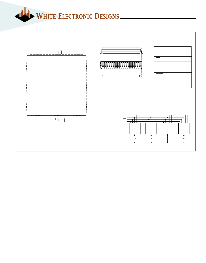
PIN CONFIGURATION FOR WF1M32B-XHX3
PIN DESCRIPTION
TOP VIEW
I/O
0-31
Data Inputs/Outputs
A
0-19
Address Inputs
WE
Write Enable
CS
1-4
Chip Selects
OE
Output Enable
RESET
Reset
V
CC
Power Supply
GND
Ground
NC
Not Connected
BLOCK DIAGRAM
1M x 8
8
I / O 0 - 7
CS1
1M x 8
8
I / O 8 - 1 5
CS2
1M x 8
8
I / O 1 6 - 2 3
CS3
1M x 8
8
I / O 2 4 - 3 1
CS4
A 0 - 1 9
O E
W E
RESET
2
White Electronic Designs Corporation ∑ Phoenix, AZ ∑ (602) 437-1520
WF1M32B-XXX3
10
11
12
13
14
15
16
17
18
19
20
21
22
23
24
25
26
60
59
58
57
56
55
54
53
52
51
50
49
48
47
46
45
44
9 8 7 6 5 4 3 2 1 68 67 66 65 64 63 62 61
27 28 29 30 31 32 33 34 35 36 37 38 39 40 41 42 43
I/O
0
I/O
1
I/O
2
I/O
3
I/O
4
I/O
5
I/O
6
I/O
7
GND
I/O
8
I/O
9
I/O
10
I/O
11
I/O
12
I/O
13
I/O
14
I/O
15
V
CC
A
11
A
12
A
13
A
14
A
15
A
16
CS
1
OE
CS
2
A
17
WE
2
WE
3
WE
4
A
18
A
19
NC
I/O
16
I/O
17
I/O
18
I/O
19
I/O
20
I/O
21
I/O
22
I/O
23
GND
I/O
24
I/O
25
I/O
26
I/O
27
I/O
28
I/O
29
I/O
30
I/O
31
RESE
T
A
0
A
1
A
2
A
3
A
4
A
5
CS
3
GND
CS
4
WE
1
A
6
A
7
A
8
A
9
A
10
V
CC
PIN CONFIGURATION FOR WF1M32B-XG2TX3
PIN DESCRIPTION
TOP VIEW
I/O
0-31
Data Inputs/Outputs
A
0-19
Address Inputs
WE
1-4
Write Enables
CS
1-4
Chip Selects
OE
Output Enable
RESET
Reset/Powerdown
V
CC
Power Supply
GND
Ground
The White 68 lead G2T CQFP
fills the same fit and function as
the JEDEC 68 lead CQFJ or 68
PLCC. But the G2T has the TCE
and lead inspection advantage
of the CQFP form.
0.940"
1M x 8
8
I / O
0 - 7
CS
1
1M x 8
8
I / O
8 - 1 5
CS
2
1M x 8
8
I / O
1 6 - 2 3
CS
3
1M x 8
8
I / O
2 4 - 3 1
CS
4
A 0 - 1 9
O E
WE
3
WE
2
WE
1
WE
4
R E S E T
BLOCK DIAGRAM

3
White Electronic Designs Corporation ∑ Phoenix, AZ ∑ (602) 437-1520
WF1M32B-XXX3
ABSOLUTE MAXIMUM RATINGS
NOTES:
1. Stresses above the absolute maximum rating may cause permanent damage
to the device. Extended operation at the maximum levels may degrade
performance and affect reliability.
Parameter
Unit
Operating Temperature
-55 to +125
∞
C
Supply Voltage Range (V
CC
)
-0.5 to +4.0
V
Signal Voltage Range
-0.5 to Vcc +0.5
V
Storage Temperature Range
-65 to +150
∞
C
Lead Temperature (soldering, 10 seconds)
+300
∞
C
Endurance (write/erase cycles)
1,000,000 min.
cycles
RECOMMENDED OPERATING CONDITIONS
Parameter
Symbol
Min
Max
Unit
Supply Voltage
V
CC
3.0
3.6
V
Input High Voltage
V
IH
0.7 x Vcc
V
CC
+ 0.3
V
Input Low Voltage
V
IL
-0.5
+0.8
V
Operating Temp. (Mil.)
T
A
-55
+125
∞
C
Operating Temp. (Ind.)
T
A
-40
+85
∞
C
CAPACITANCE
(T
A
= +25
∞
C)
Parameter
Symbol
Conditions
Max
Unit
OE capacitance
C
OE
V
IN
= 0 V, f = 1.0 MHz
50
pF
WE
1-4
capacitance
C
WE
V
IN
= 0 V, f = 1.0 MHz
20
pF
CS
1-4
capacitance
C
CS
V
IN
= 0 V, f = 1.0 MHz
20
pF
Data I/O capacitance
C
I/O
V
I/O
= 0 V, f = 1.0 MHz
20
pF
Address input capacitance
C
AD
V
IN
= 0 V, f = 1.0 MHz
50
pF
This parameter is guaranteed by design but not tested.
Parameter
Symbol
Conditions
Min
Max
Unit
Input Leakage Current
I
LI
V
CC
= 3.6, V
IN
= GND or V
CC
10
µ
A
Output Leakage Current
I
LOx32
V
CC
= 3.6, V
IN
= GND or V
CC
10
µ
A
V
CC
Active Current for Read (1)
I
CC1
CS = V
IL
, OE = V
IH
, f = 5MHz
120
mA
V
CC
Active Current for Program or Erase (2)
I
CC2
CS = V
IL
, OE = V
IH
140
mA
V
CC
Standby Current
I
CC3
V
CC
= 3.6, CS = V
IH
, f = 5MHz
200
µ
A
Output Low Voltage
V
OL
I
OL
= 5.8 mA, V
CC
= 3.0
0.45
V
Output High Voltage
V
OH1
I
OH
= -2.0 mA, V
CC
= 3.0
0.85
X
V
CC
V
Low V
CC
Lock-Out Voltage (4)
V
LKO
2.3
2.5
V
DC CHARACTERISTICS - CMOS COMPATIBLE
(V
CC
= 3.3V, V
SS
= 0V, T
A
= -55
∞
C to +125
∞
C)
NOTES:
1. The I
CC
current listed includes both the DC operating current and the frequency dependent component (at 5 MHz). The frequency component typically
is less than 8 mA/MHz, with OE at V
IH
.
2. I
CC
active while Embedded Algorithm (program or erase) is in progress.
3. DC test conditions: V
IL
= 0.3V, V
IH
= V
CC
- 0.3V
4. Guaranteed by design, but not tested.
DATA RETENTION
Parameter
Test Conditions
Min
Unit
Minimum Pattern Data
150
∞
C
10
Years
Retention Time
125
∞
C
20
Years

4
White Electronic Designs Corporation ∑ Phoenix, AZ ∑ (602) 437-1520
WF1M32B-XXX3
AC CHARACTERISTICS ≠ WRITE/ERASE/PROGRAM OPERATIONS,CS CONTROLLED
(V
CC
= 3.3V, V
SS
= 0V, T
A
= -55
∞
C to +125
∞
C)
Parameter
Symbol
-100
-120
-150
Unit
Min
Max
Min
Max
Min
Max
Write Cycle Time
t
AVAV
t
WC
100
120
150
ns
Write Enable Setup Time
t
WLEL
t
WS
0
0
0
ns
Chip Select Pulse Width
t
ELEH
t
CP
45
50
50
ns
Address Setup Time
t
AVEL
t
AS
0
0
0
ns
Data Setup Time
t
DVEH
t
DS
45
50
50
ns
Data Hold Time
t
EHDX
t
DH
0
0
0
ns
Address Hold Time
t
ELAX
t
AH
45
50
50
ns
Chip Select Pulse Width High
t
EHEL
t
CPH
20
20
20
ns
Duration of Byte Programming Operation (1)
t
WHWH1
300
300
300
µ
s
Sector Erase Time
t
WHWH2
15
15
15
sec
Read Recovery Time (2)
t
GHEL
0
0
0
µ
s
Chip Programming Time
50
50
50
sec
1. Typical value for t
WHWH1
is 9
µ
s.
2. Guaranteed by design, but not tested.
AC TEST CIRCUIT
AC TEST CONDITIONS
NOTES:
V
Z
is programmable from -2V to +7V.
I
OL
& I
OH
programmable from 0 to 16mA.
Tester Impedance Z
0
= 75
.
V
Z
is typically the midpoint of V
OH
and V
OL
.
I
OL
& I
OH
are adjusted to simulate a typical resistive load circuit.
ATE tester includes jig capacitance.
Parameter
Typ
Unit
Input Pulse Levels
V
IL
= 0, V
IH
= 2.5
V
Input Rise and Fall
5
ns
Input and Output Reference Level
1.5
V
Output Timing Reference Level
1.5
V
I
Current Source
D.U.T.
C = 50 pf
eff
I
OL
V
1.5V
(Bipolar Supply)
Z
Current Source
OH

5
White Electronic Designs Corporation ∑ Phoenix, AZ ∑ (602) 437-1520
WF1M32B-XXX3
AC CHARACTERISTICS ≠ WRITE/ERASE/PROGRAM OPERATIONS - WE CONTROLLED
(V
CC
= 3.3V, T
A
= -55
∞
C to +125
∞
C)
Parameter
Symbol
-100
-120
-150
Unit
Min
Max
Min
Max
Min
Max
Write Cycle Time
t
AVAV
t
WC
100
120
150
ns
Chip Select Setup Time
t
ELWL
t
CS
0
0
0
ns
Write Enable Pulse Width
t
WLWH
t
WP
50
50
65
ns
Address Setup Time
t
AVWL
t
AS
0
0
0
ns
Data Setup Time
t
DVWH
t
DS
50
50
65
ns
Data Hold Time
t
WHDX
t
DH
0
0
0
ns
Address Hold Time
t
WLAX
t
AH
50
50
65
ns
Write Enable Pulse Width High
t
WHWL
t
WPH
30
30
35
ns
Duration of Byte Programming Operation (1)
t
WHWH1
300
300
300
µ
s
Sector Erase
t
WHWH2
15
15
15
sec
Read Recovery Time before Write (3)
t
GHWL
0
0
0
µ
s
V
CC
Setup Time
t
VCS
50
50
50
µ
s
Chip Programming Time
50
50
50
sec
Output Enable Setup Time
t
OES
0
0
0
ns
Output Enable Hold Time (2)
t
OEH
10
10
10
ns
1. Typical value for t
WHWH1
is 9
µ
s.
2. For Toggle and Data Polling.
3. Guaranteed by design, but not tested.
AC CHARACTERISTICS ≠ READ-ONLY OPERATIONS
(V
CC
= 3.3V, T
A
= -55
∞
C to +125
∞
C)
Parameter
Symbol
-100
-120
-150
Unit
Min
Max
Min
Max
Min
Max
Read Cycle Time
t
AVAV
t
RC
100
120
150
ns
Address Access Time
t
AVQV
t
ACC
100
120
150
ns
Chip Select Access Time
t
ELQV
t
CE
100
120
150
ns
Output Enable to Output Valid
t
GLQV
t
OE
40
50
55
ns
Chip Select High to Output High Z (1)
t
EHQZ
t
DF
30
30
40
ns
Output Enable High to Output High Z (1)
t
GHQZ
t
DF
30
30
40
ns
Output Hold from Addresses, CS or OE Change,
t
AXQX
t
OH
0
0
0
ns
whichever is First
1. Guaranteed by design, not tested.
6
White Electronic Designs Corporation ∑ Phoenix, AZ ∑ (602) 437-1520
WF1M32B-XXX3
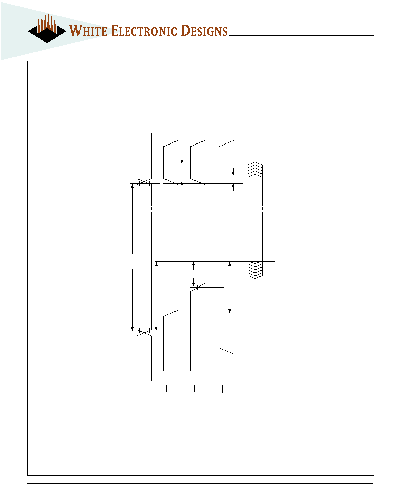
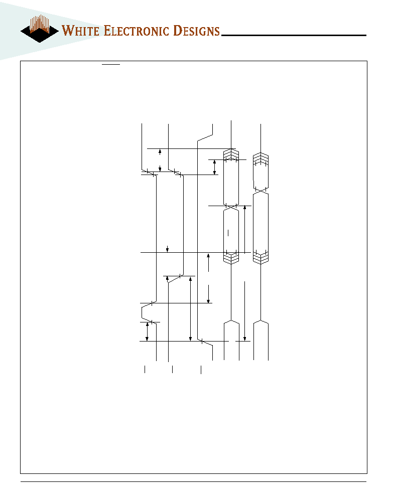
AC WAVEFORMS FOR READ OPERATIONS
Addresses
CS
OE
WE
Outputs
High Z
Addresses Stable
t
OE
t
RC
Output Valid
t
CE
t
ACC
t
OH
High Z
t
DF
7
White Electronic Designs Corporation ∑ Phoenix, AZ ∑ (602) 437-1520
WF1M32B-XXX3
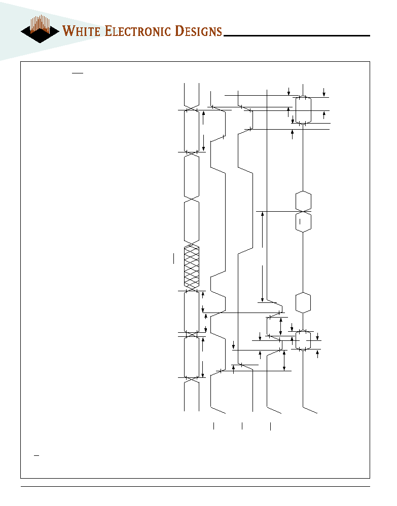
NOTES:
1. PA is the address of the memory location to be programmed.
2. PD is the data to be programmed at byte address.
3. D
7
is the output of the complement of the data written to each chip.
4. D
OUT
is the output of the data written to the device.
5. Figure indicates last two bus cycles of four bus cycle sequence.
WRITE/ERASE/PROGRAM
OPERATION, WE CONTROLLED
Addresses
CS
OE
WE
Data
AAAH
PA
PA
t
WC
t
CS
PD
D
7
D
OUT
t
AH
t
WPH
t
DH
t
DS
Data Polling
t
AS
t
RC
t
WP
A0H
t
OE
t
DF
t
OH
t
GHWL
t
WHWH1
8
White Electronic Designs Corporation ∑ Phoenix, AZ ∑ (602) 437-1520
WF1M32B-XXX3
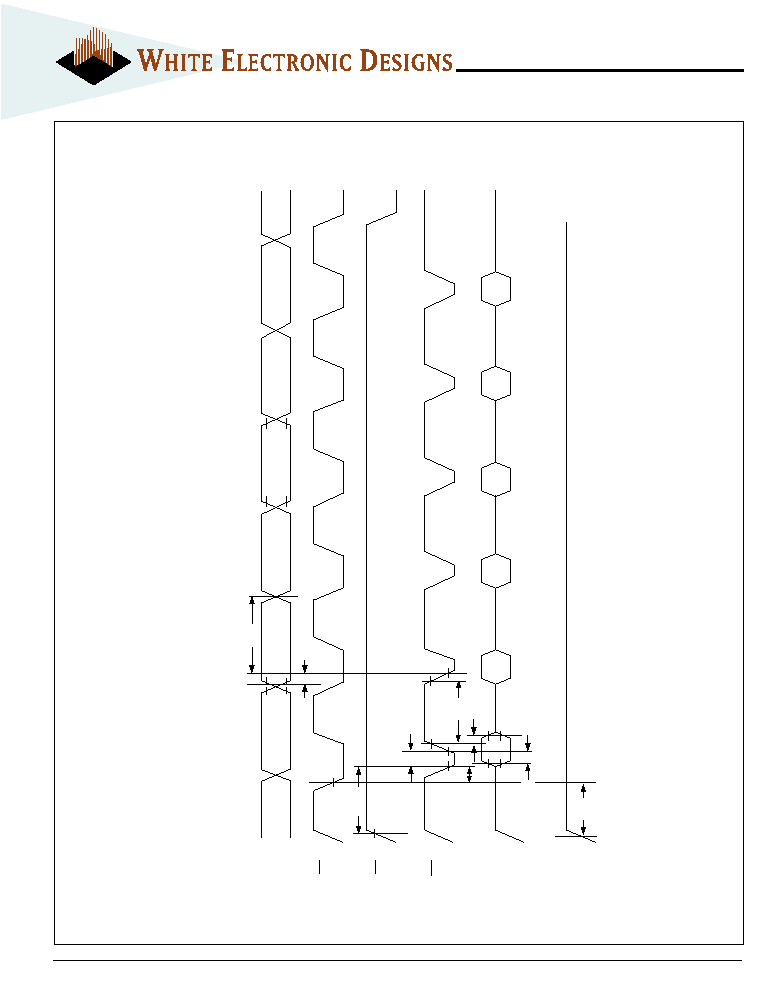
AC WAVEFORMS CHIP/SECTOR
ERASE OPERATIONS
NOTE:
1. SA is the sector address for Sector Erase.
Addresses
CS
OE
WE
Data
V
CC
AAAH
555H
555H
SA
AAAH
AAAH
t
WP
t
CS
t
VCS
10H/30H
55H
80H
55H
AAH
AAH
t
AH
t
GHWL
t
WPH
t
DH
t
DS
t
AS
9
White Electronic Designs Corporation ∑ Phoenix, AZ ∑ (602) 437-1520
WF1M32B-XXX3
AC WAVEFORMS FOR DATA POLLING
DURING EMBEDDED ALGORITHM OPERATIONS
CS
OE
WE
t
OE
t
CE
t
CH
t
OH
D7
D7 =
Valid Data
High Z
D0-D6 = Invalid
D0-D7
Valid Data
t
DF
D7
D0-D6
t
OEH
t
WHWH 1 or 2
Data

10
White Electronic Designs Corporation ∑ Phoenix, AZ ∑ (602) 437-1520
WF1M32B-XXX3
NOTES:
1. PA represents the address of the memory location to be programmed.
2. PD represents the data to be programmed at byte address.
3. D
7
is the output of the complement of the data written to each chip.
4. D
OUT
is the output of the data written to the device.
5. Figure indicates the last two bus cycles of a four bus cycle sequence.
Addresses
WE
OE
CS
Data
AAAH
PA
PA
t
WC
t
WS
PD
D
7
D
OUT
t
AH
t
CPH
t
CP
t
DH
t
DS
Data Polling
t
AS
t
GHEL
A0H
t
WHWH1
ALTERNATE CS CONTROLLED
PROGRAMMING OPERATION TIMINGS
11
White Electronic Designs Corporation ∑ Phoenix, AZ ∑ (602) 437-1520
WF1M32B-XXX3
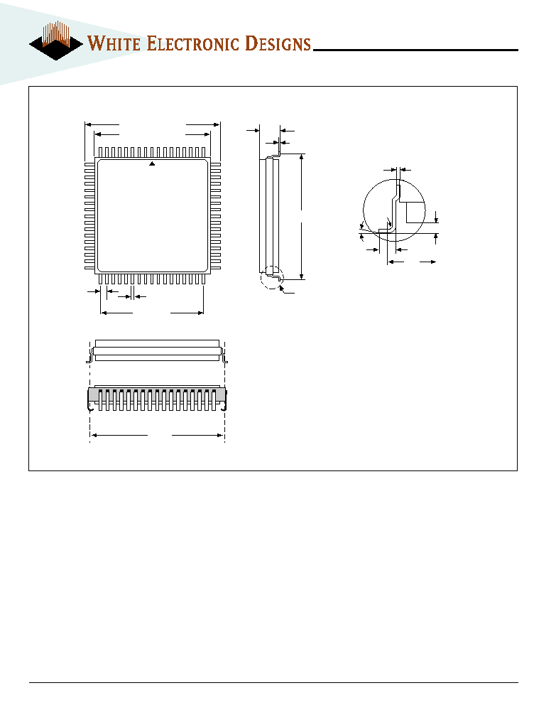
PACKAGE 509:
68 LEAD, LOW PROFILE CERAMIC QUAD FLAT PACK, CQFP (G2T)
0.38 (0.015)
±
0.05 (0.002)
0.27 (0.011)
±
0.04 (0.002)
25.15 (0.990)
±
0.26 (0.010) SQ
1.27 (0.050) TYP
24.03 (0.946)
±
0.26 (0.010)
22.36 (0.880)
±
0.26 (0.010) SQ
20.3 (0.800) REF
4.57 (0.180) MAX
0.19 (0.007)
±
0.06 (0.002)
23.87
(0.940) REF
1.0 (0.040)
±
0.127 (0.005)
0.25 (0.010) REF
1
∞
/ 7
∞
R 0.25
(0.010)
DETAIL A
SEE DETAIL "A"
Pin 1
ALL LINEAR DIMENSIONS ARE MILLIMETERS AND PARENTHETICALLY IN INCHES
0.940"
TYP
The White 68 lead G2T CQFP
fills the same fit and function as
the JEDEC 68 lead CQFJ or 68
PLCC. But the G2T has the TCE
and lead inspection advantage
of the CQFP form.
12
White Electronic Designs Corporation ∑ Phoenix, AZ ∑ (602) 437-1520
WF1M32B-XXX3
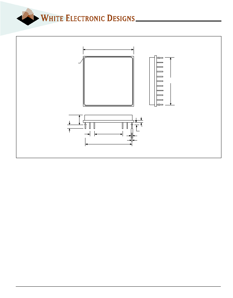
PACKAGE 401:
66 PIN, PGA TYPE, CERAMIC HEX-IN-LINE PACKAGE, HIP (H)
30.1 (1.185)
±
0.38 (0.015) SQ
25.4 (1.0) TYP
15.24 (0.600) TYP
0.76 (0.030)
±
0.1 (0.005)
6.22 (0.245)
MAX
3.81 (0.150)
±
0.1 (0.005)
2.54 (0.100)
TYP
25.4 (1.0) TYP
1.27 (0.050)
±
0.1 (0.005)
1.27 (0.050) TYP DIA
0.46 (0.018)
±
0.05 (0.002) DIA
PIN 1 IDENTIFIER
SQUARE PAD
ON BOTTOM
ALL LINEAR DIMENSIONS ARE MILLIMETERS AND PARENTHETICALLY IN INCHES

13
White Electronic Designs Corporation ∑ Phoenix, AZ ∑ (602) 437-1520
WF1M32B-XXX3
ORDERING INFORMATION
LEAD FINISH:
Blank = Gold plated leads
A = Solder dip leads
PROGRAMMING VOLTAGE
3 = 3.3V
DEVICE GRADE:
M = Military Screened
-55
∞
C to +125
∞
C
I = Industrial
-40
∞
C to +85
∞
C
C = Commercial
0
∞
C to +70
∞
C
PACKAGE TYPE:
H = Ceramic Hex In line Package, HIP (Package 401)
G2T = 22mm Ceramic Quad Flat Pack, Low Profile CQFP (Package 509)
ACCESS TIME (ns)
IMPROVEMENT MARK
B = Boot Block (Bottom Sector)
ORGANIZATION, 1M x 32
User configurable as 2M x 16 or 4M x 8
Flash
WHITE ELECTRONIC DESIGNS CORP.
W F 1M32 B - XXX X X 3 X