White Microelectronics ∑ Phoenix, AZ ∑ (602) 437-1520
7
FLASH MODULES
1
WF128K16, WF256K16-XCX5
FEATURES
s Access Times of 50, 60, 70, 90, 120 and 150ns
s 40 pin Ceramic DIP (Package 303)
s Organized as 128Kx16 and 256Kx16
s Sector Architecture
∑ 8 equal size sectors of 16KBytes each per chip
∑ Any combination of sectors can be concurrently erased.
Also supports full chip erase
s 100,000 Erase/Program Cycles Minimum (0
∞
C to 70
∞
C)
s Data Retention, 10 Years at 125
∞
C
s Commercial, Industrial and Military Temperature Ranges
5V FLASH MODULE
PRELIMINARY *
s 5 Volt Programming; 5V
±
10% Supply
s Low Power CMOS
s Embedded Erase and Program Algorithms
s TTL Compatible Inputs and CMOS Outputs
s Built-in Decoupling Caps and Multiple Ground Pins for Low
Noise Operation
s Page Program Operation and Internal Program Control Time
* This data sheet describes a product under development, not fully
characterized, and is subject to change without notice.
Note: Programming information available upon request.
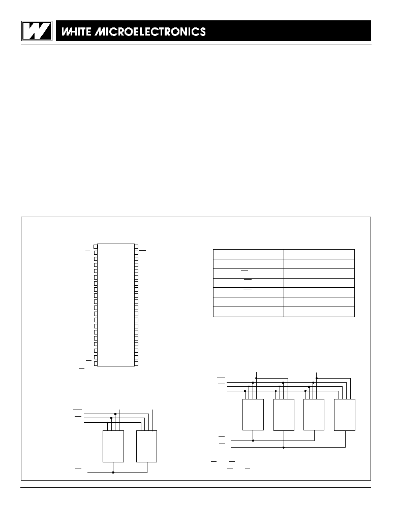
FIG. 1
PIN CONFIGURATION AND BLOCK DIAGRAM
A
0
-
16
Address Inputs
I/O
0-15
Data Input/Output
CS
1
-
2
Chip Selects
OE
Output Enable
WE
Write Enable
V
CC
+5.0V Power
GND
Ground
PIN DESCRIPTION
128K x 8
128K x 8
A
0 - 1 6
O E
W E
C S
1
C S
2
128K x 8
128K x 8
I / O
8 - 1 5
I / O
0 - 7
(1)
(1)
NOTE:
1. CS
1
and CS
2
are used to select the lower and upper 128Kx16 of the
device. CS
1
and CS
2
must not be enabled at the same time.
BLOCK DIAGRAM
FOR WF256K16-XCX5
BLOCK DIAGRAM
FOR WF128K16-XCX5
TOP VIEW
1
2
3
4
5
6
7
8
9
10
11
12
13
14
15
16
17
18
19
20
40
39
38
37
36
35
34
33
32
31
30
29
28
27
26
25
24
23
22
21
CS2*/NC
CS1
I/O15
I/O14
I/O13
I/O12
I/O11
I/O10
I/O9
I/O8
GND
I/O7
I/O6
I/O5
I/O4
I/O3
I/O2
I/O1
I/O0
OE
V
CC
WE
A16
A15
A14
A13
A12
A11
A10
A9
GND
A8
A7
A6
A5
A4
A3
A2
A1
A0
128K x 8
A
0 - 1 6
O E
W E
C S
1
128K x 8
I / O
8 - 1 5
I / O
0 - 7
* CS
2
for 256Kx16 and NC for 128Kx16
October 1998
2
White Microelectronics ∑ Phoenix, AZ ∑ (602) 437-1520
7
FLASH MODULES
WF128K16, WF256K16-XCX5
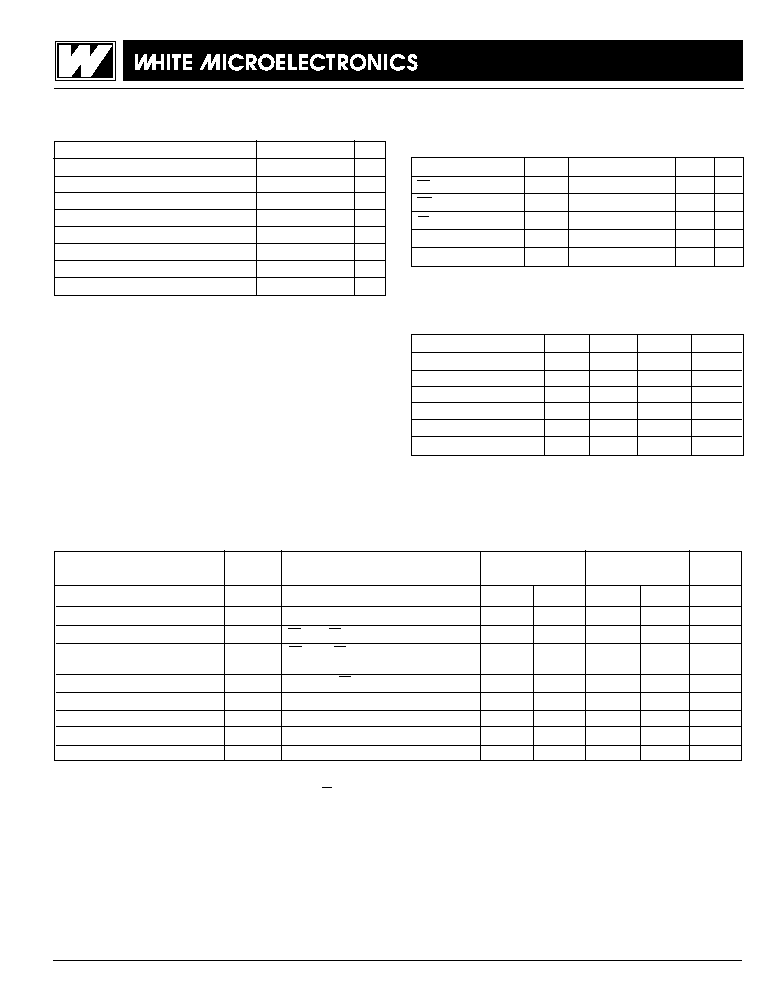
ABSOLUTE MAXIMUM RATINGS (1)
NOTES:
1. Stresses above the absolute maximum rating may cause permanent damage
to the device. Extended operation at the maximum levels may degrade
performance and affect reliability.
2. Minimum DC voltage on input or I/O pins is -0.5V. During voltage transitions,
inputs may overshoot V
SS
to -2.0 V for periods of up to 20ns. Maximum DC
voltage on output and I/O pins is V
CC
+ 0.5V. During voltage transitions,
outputs may overshoot to Vcc + 2.0 V for periods of up to 20ns.
3. Minimum DC input voltage on A
9
pin is -0.5V. During voltage transitions, A
9
may
overshoot Vss to -2V for periods of up to 20ns. Maximum DC input voltage on A
9
is +13.5V which may overshoot to 14.0 V for periods up to 20ns.
CAPACITANCE
(T
A
= 25
∞
C)
DC CHARACTERISTICS - CMOS COMPATIBLE
(V
CC
= 5.0V, V
SS
= 0V, T
A
= -55
∞
C to +125
∞
C)
Parameter
Unit
Operating Temperature
-55 to +125
∞
C
Supply Voltage Range (V
CC
)
-2.0 to +7.0
V
Signal voltage range (any pin except A9) (2)
-2.0 to +7.0
V
Storage Temperature Range
-65 to +150
∞
C
Lead Temperature (soldering, 10 seconds)
+300
∞
C
Data Retention Mil Temp
10 years
Endurance (write/erase cycles) Mil Temp
10,000 cycles min.
A
9
Voltage for sector protect (V
ID
) (3)
-2.0 to +14.0
V
NOTES:
1. The I
CC
current listed includes both the DC operating current and the frequency dependent component (at 5 MHz).
The frequency component typically is less than 2 mA/MHz, with OE at V
IH
.
2. I
CC
active while Embedded Algorithm (program or erase) is in progress.
3. DC test conditions: V
IL
= 0.3V, V
IH
= V
CC
- 0.3V
Parameter
Symbol
Conditions
128K x 16
256K x 16
Unit
Min
Max
Min
Max
Input Leakage Current
I
LI
V
CC
= 5.5, V
IN
= GND to V
CC
10
10
µ
A
Output Leakage Current
I
LO
V
CC
= 5.5, V
IN
= GND to V
CC
10
10
µ
A
V
CC
Active Current for Read
(1)
I
CC1
CS = V
IL
, OE = V
IH
70
80
mA
V
CC
Active Current for Program
I
CC2
CS = V
IL
, OE = V
IH
100
110
mA
or Erase
(2)
V
CC
Standby Current
I
CC3
V
CC
= 5.5, CS = V
IH
, f = 5MHz
6
8
mA
Output Low Voltage
V
OL
I
OL
= 12.0 mA, V
CC
= 4.5
0.45
0.45
V
Output High Voltage
V
OH1
I
OH
= -2.5 mA, V
CC
= 4.5
0.85xVcc
0.85xVcc
V
Output High Voltage
V
OH2
I
OH
= -100
µ
A, V
CC
= 4.5
V
CC
-0.4
V
CC -0.4
V
Low V
CC
Lock Out Voltage
V
LKO
3.2
3.2
V
Test
Symbol
Conditions
Max
Unit
OE capacitance
C
OE
V
IN
= 0 V, f = 1.0 MHz
50
pF
WE capacitance
C
WE
V
IN
= 0 V, f = 1.0 MHz
50
pF
CS capacitance
C
CS
V
IN
= 0 V, f = 1.0 MHz
30
pF
I/O
0-7
capacitance
C
I/O
V
I/O
= 0 V, f = 1.0 MHz
30
pF
Address capacitance
C
AD
V
IN
= 0 V, f = 1.0 MHz 50
pF
This parameter is guaranteed by design but not tested.
RECOMMENDED OPERATING CONDITIONS
Parameter
Symbol
Min
Max
Unit
Supply Voltage
V
CC
4.5
5.5
V
Input High Voltage
V
IH
2.0
V
CC
+ 0.3
V
Input Low Voltage
V
IL
-0.5
+0.8
V
Operating Temp. (Mil.)
T
A
-55
+125
∞
C
Operating Temp. (Ind.)
T
A
-40
+85
∞
C
A
9
Voltage for Sector Protect
V
ID
11.5
12.5
V
White Microelectronics ∑ Phoenix, AZ ∑ (602) 437-1520
7
FLASH MODULES
3
WF128K16, WF256K16-XCX5
PRINCIPLES OF OPERATION
WRITE
Device erasure and programming are accomplished via the
command register. The contents of the register serve as input
to the internal state machine. The state machine outputs
dictate the function of the device.
The command register itself does not occupy an addressable
memory location. The register is a latch used to store the
commands, along with address and data information needed to
execute the command. The command register is written by
bringing Write-Enable to a logic-low level (V
IL
), while Chip-Select
is low and OE is at V
IH
. Addresses are latched on the falling edge
of the Write-Enable while data is latched on the rising edge of the
WE pulse. Standard microprocessor write timings are used. Refer
to AC Program characteristics, Figures 4 and 7.
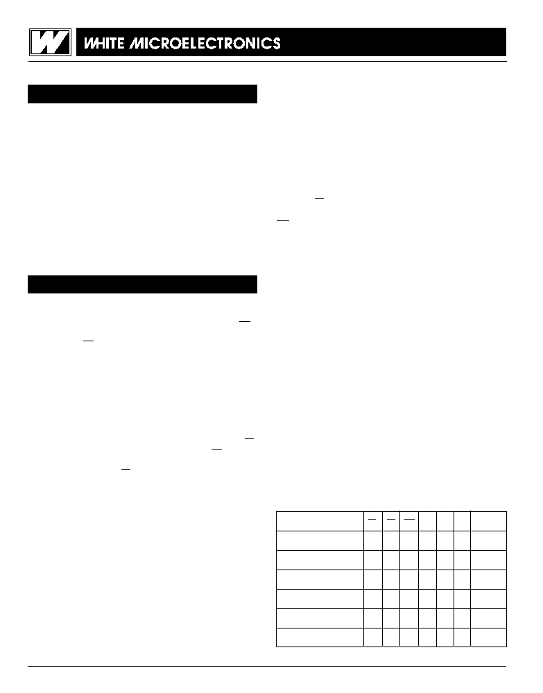
TABLE 1 - BUS OPERATIONS
Operation
CS
OE
WE
A
0
A
1
A
9
I/O
Read
L
L
H
A
0
A
1
A
9
D
OUT
Standby
H
X
X
X
X
X
HIGH Z
Output Disable
L
H
H
X
X
X
HIGH Z
Write
L
H
L
A
0
A
1
A
9
D
IN
Enable Sector Protect
L
V
ID
L
X
X
V
ID
X
Verify Sector Protect
L
L
H
L
H
V
ID
Code
The following principles of operation of the WF128K16-XCX5
and WF256K16-XCX5 are applicable to each 128K x 8 memory
chip inside the MCM. Programming of the device is accom-
plished by executing the program command sequence. The
program algorithm, which is an internal algorithm, automati-
cally times the program pulse widths and verifies proper cell
margin. Sectors can be programmed and verified in less than 0.3
seconds. Erase is accomplished by executing the erase
command sequence. The erase algorithm, which is internal,
automatically preprograms the array if it is not already
programmed before executing the erase operation. During
erase, the device automatically times the erase pulse widths
and verifies proper cell margin. The entire memory is typically
erased and verified in three seconds (including pre-program-
ming).
BUS OPERATIONS
READ
The device has two control functions, both of which must be
logically active, to obtain data at the outputs. Chip-Select (CS)
is the power control and should be used for device selection.
Output-Enable (OE) is the output control and should be used to
gate data to the output pins. Figure 3 illustrates read timing
waveforms.
OUTPUT DISABLE
With Output-Enable at a logic-high level (V
IH
), output from the
device is disabled. Output pins are placed in a high
impedance state.
STANDBY MODE
The device has two standby modes, a CMOS standby mode (CS
input held at V
CC
+ 0.5V), and a TTL standby mode (CS is held
V
IH
). In the standby mode the outputs are in a high impedance
state, independent of the OE input.
If the device is deselected during erasure or programming, the
device will draw active current until the operation is completed.
4
White Microelectronics ∑ Phoenix, AZ ∑ (602) 437-1520
7
FLASH MODULES
WF128K16, WF256K16-XCX5
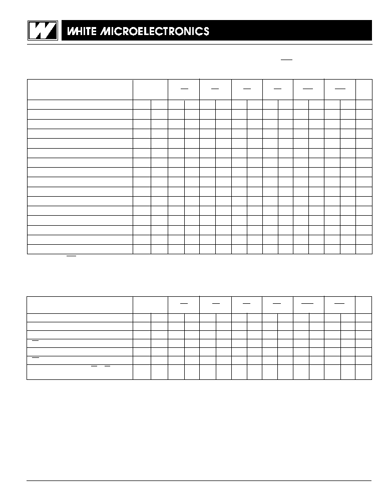
AC CHARACTERISTICS ≠ WRITE/ERASE/PROGRAM OPERATIONS, WE CONTROLLED
(V
CC
= 5.0V, V
SS
= 0V, T
A
= -55
∞
C to +125
∞
C)
Parameter
Symbol
-50
-60
-70
-90
-120
-150
Unit
Min
Max
Min
Max
Min
Max
Min
Max
Min
Max
Min
Max
Write Cycle Time
t
AVAV
t
WC
50
60
70
90
120
150
ns
Chip Select Setup Time
t
ELWL
t
CS
0
0
0
0
0
0
ns
Write Enable Pulse Width
t
WLWH
t
WP
25
30
35
45
50
50
ns
Address Setup Time
t
AVWL
t
AS
0
0
0
0
0
0
ns
Data Setup Time
t
DVWH
t
DS
25
30
30
45
50
50
ns
Data Hold Time
t
WHDX
t
DH
0
0
0
0
0
0
ns
Address Hold Time
t
WLAX
t
AH
40
45
45
45
50
50
ns
Chip Select Hold Time
t
WHEH
t
CH
0
0
0
0
0
0
ns
Write Enable Pulse Width High
t
WHWL
t
WPH
20
20
20
20
20
20
ns
Duration of Byte Programming Operation (min)
t
WHWH1
14
14
14
14
14
14
µ
s
Chip and Sector Erase Time
t
WHWH2
2.2
60
2.2
60
2.2
60
2.2
60
2.2
60
2.2
60
sec
Read Recovery Time Before Write
t
GHWL
0
0
0
0
0
0
ns
V
CC
Setup Time
t
VCS
50
50
50
50
50
50
µ
s
Chip Programming Time
12.5
12.5
12.5
12.5
12.5
12.5
sec
Output Enable Setup Time
t
OES
0
0
0
0
0
0
ns
Output Enable Hold Time (1)
t
OEH
10
10
10
10
10
10
ns
1. For Toggle and Data Polling.
AC CHARACTERISTICS ≠ READ ONLY OPERATIONS
(V
CC
= 5.0V, V
SS
= 0V, T
A
= -55
∞
C to +125
∞
C)
Parameter
Symbol
-50
-60
-70
-90
-120
-150
Unit
Min
Max
Min
Max
Min
Max
Min Max
Min
Max
Min
Max
Read Cycle Time
t
AVAV
t
RC
50
60
70
90
120
150
ns
Address Access Time
t
AVQV
t
ACC
50
60
70
90
120
150
ns
Chip Select Access Time
t
ELQV
t
CE
50
60
70
90
120
150
ns
OE to Output Valid
t
GLQV
t
OE
25
30
35
40
50
55
ns
Chip Select to Output High Z (1)
t
EHQZ
t
DF
20
20
20
25
30
35
ns
OE High to Output High Z (1)
t
GHQZ
t
DF
20
20
20
25
30
35
ns
Output Hold from Address, CS or OE Change,
t
AXQX
t
OH
0
0
0
0
0
0
ns
whichever is first
1. Guaranteed by design, not tested.
White Microelectronics ∑ Phoenix, AZ ∑ (602) 437-1520
7
FLASH MODULES
5
WF128K16, WF256K16-XCX5
AC CHARACTERISTICS ≠ WRITE/ERASE/PROGRAM OPERATIONS, CS CONTROLLED
(V
CC
= 5.0V, V
SS
= 0V, T
A
= -55
∞
C to +125
∞
C)
Parameter
Symbol
-50
-60
-70
-90
-120
-150
Unit
Min
Max
Min
Max
Min
Max Min
Max
Min
Max
Min
Max
Write Cycle Time
t
AVAV
t
WC
50
60
70
90
120
150
ns
WE Setup Time
t
WLEL
t
WS
0
0
0
0
0
0
ns
CS Pulse Width
t
ELEH
t
CP
25
30
35
45
50
50
ns
Address Setup Time
t
AVEL
t
AS
0
0
0
0
0
0
ns
Data Setup Time
t
DVEH
t
DS
25
30
30
45
50
50
ns
Data Hold Time
t
EHDX
t
DH
0
0
0
0
0
0
ns
Address Hold Time
t
ELAX
t
AH
40
45
45
45
50
50
ns
WE Hold from WE High
t
EHWH
t
WH
0
0
0
0
0
0
ns
CS Pulse Width High
t
EHEL
t
CPH
20
20
20
20
20
20
ns
Duration of Programming Operation
t
WHWH1
14
14
14
14
14
14
µ
s
Duration of Erase Operation
t
WHWH2
2.2
60
2.2
60
2.2
60
2.2
60
2.2
60
2.2
60
sec
Read Recovery before Write
t
GHEL
0
0
0
0
0
0
ns
Chip Programming Time
12.5
12.5
12.5
12.5
12.5
12.5
sec
FIG. 2
AC TEST CIRCUIT
NOTES:
V
Z
is programmable from -2V to +7V.
I
OL
& I
OH
programmable from 0 to 16mA.
Tester Impedance Z
0
= 75
.
V
Z
is typically the midpoint of V
OH
and V
OL
.
I
OL
& I
OH
are adjusted to simulate a typical resistive load circuit.
ATE tester includes jig capacitance.
AC TEST CONDITIONS
I
Current Source
D.U.T.
C = 50 pf
eff
I
OL
V
1.5V
(Bipolar Supply)
Z
Current Source
OH
Parameter
Typ
Unit
Input Pulse Levels
V
IL
= 0, V
IH
= 3.0 V
Input Rise and Fall
5
ns
Input and Output Reference Level
1.5
V
Output Timing Reference Level
1.5
V