
1
White Electronic Designs Corporation ∑ (602) 437-1520 ∑ www.wedc.com
White Electronic Designs
WF2M32-XXX5
October 2004
Rev. 5
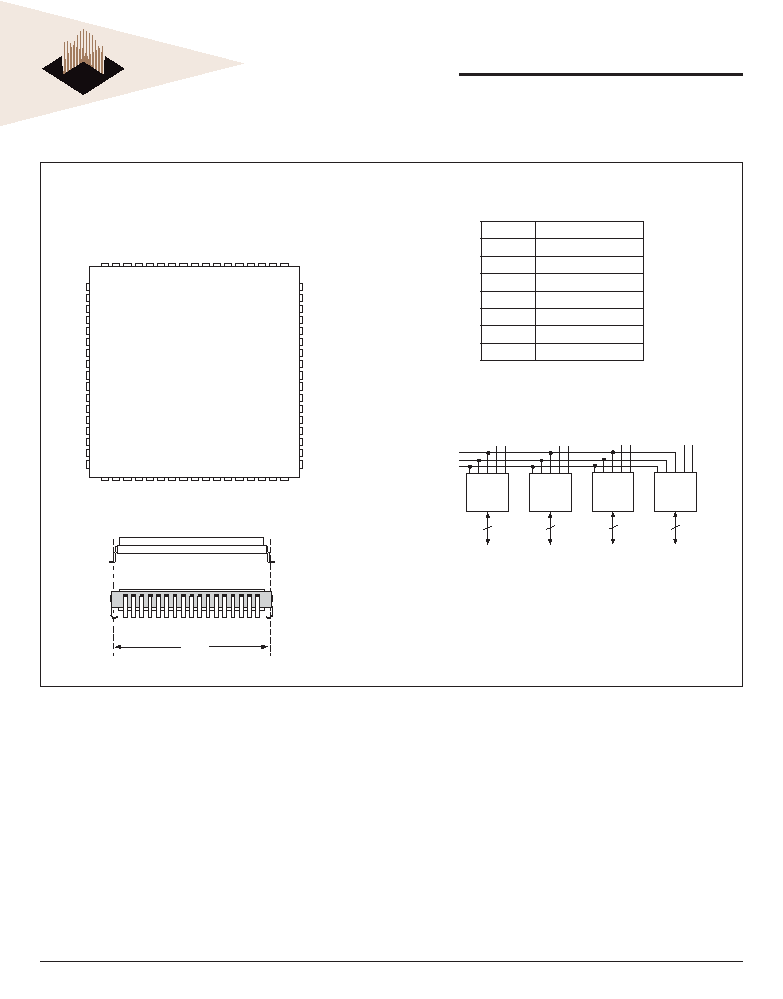
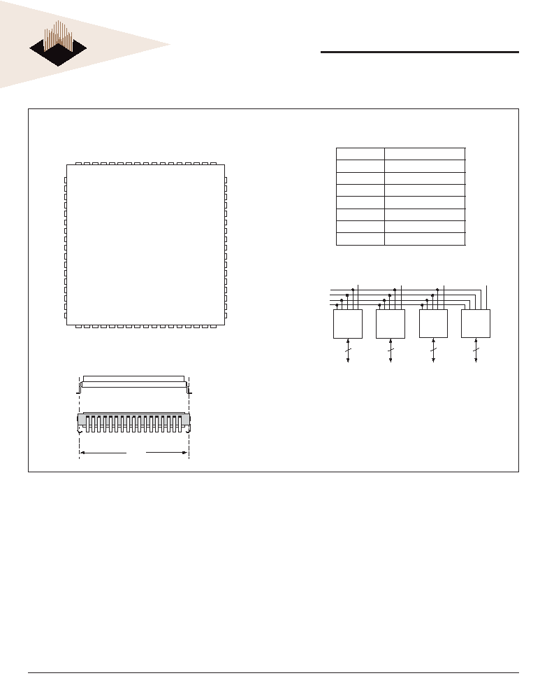
FIGURE 1 ≠ PIN CONFIGURATION FOR WF2M32-XHX5
Top View
Block Diagram
2M x 8
8
I / O
0 - 7
2M x 8
8
I / O
8 - 1 5
2M x 8
8
I / O
1 6 - 2 3
2M x 8
8
I / O
2 4 - 3 1
A
0
-
2 0
O E #
WE1# CS1#
WE2# CS2#
WE3# CS3#
WE4# CS4#
2Mx32 5V Flash Module
Organized as 2Mx32
Commercial, Industrial, and Military
Temperature Ranges
5 Volt Read and Write. 5V ± 10% Supply.
Low
Power
CMOS
Data# Polling and Toggle Bit feature for detection of
program or erase cycle completion.
Supports reading or programming data to a sector
not being erased.
RESET# pin resets internal state machine to the
read mode.
Built in Decoupling Caps and Multiple Ground Pins
for Low Noise Operation, Separate Power and
Ground Planes to improve noise immunity
* This product is subject to change without notice.
Note: For programming information refer to Flash Programming 16M5 Application Note.
FEATURES
Access Time of 90, 120, 150ns
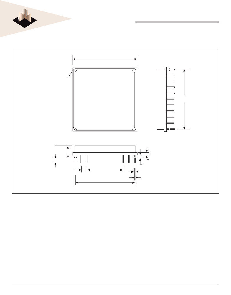
Packaging:
∑ 66 pin, PGA Type, 1.185" square, Hermetic
Ceramic HIP (Package 401).
∑ 68 lead, Hermetic CQFP (G2U), 22.4mm (0.880")
square (Package 510) 3.56mm (0.140") height.
Designed to fi t JEDEC 68 lead 0.990" CQFJ
footprint (FIGURE 3)
Sector
Architecture
∑ 32 equal size sectors of 64KBytes per each 2Mx8
chip
∑ Any combination of sectors can be erased. Also
supports full chip erase.
Minimum 100,000 Write/Erase Cycles Minimum
RESET# internally tied to V
CC
in the HIP package for this pin con-
fi guration. See Alternate Pin Confi guration with RESET# tied to pin
12 for system control of reset (FIGURE 10, page 11).
I/O
8
I/O
9
I/O
10
A
14
A
16
A
11
A
0
A
18
I/O
0
I/O
1
I/O
2
WE
2#
CS
2#
GND
I/O
11
A
10
A
9
A
15
V
CC
CS
1#
A
19
I/O
3
I/O
15
I/O
14
I/O
13
I/O
12
OE#
A
17
WE
1#
I/O
7
I/O
6
I/O
5
I/O
4
I/O
24
I/O
25
I/O
26
A
7
A
12
A
20
A
13
A
8
I/O
16
I/O
17
I/O
18
V
CC
CS
4#
WE
4#
I/O
27
A
4
A
5
A
6
WE
3#
CS
3#
GND
I/O
19
I/O
31
I/O
30
I/O
29
I/O
28
A
1
A
2
A
3
I/O
23
I/O
22
I/O
21
I/O
20
11 22 33 44 55 66
1 12 23 34 45 56
Pin Description
I/O0-31
Data Inputs/Outputs
A0-20
Address Inputs
WE1-4#
Write Enables
CS1-4#
Chip Selects
OE#
Output Enable
VCC
Power Supply
GND
Ground
2
White Electronic Designs Corporation ∑ (602) 437-1520 ∑ www.wedc.com
White Electronic Designs
WF2M32-XXX5
October 2004
Rev. 5
FIGURE 2 ≠ PIN CONFIGURATION FOR WF2M32-XG2UX5
Block Diagram
Top View
The WEDC 68 lead G2U CQFP fi lls the same fi t and function as the
JEDEC 68 lead CQFJ or 68 PLCC. But the G2U has the TCE and lead
inspection advantage of the CQFP form.
2M x 8
8
I / O
0 - 7
2M x 8
8
I / O
8 - 1 5
2M x 8
8
I / O
1 6 - 2 3
2M x 8
8
I / O
2 4 - 3 1
A
0 - 2 0
O E #
R E S E T #
WE1# CS1#
WE2# CS2#
WE3# CS3#
WE4# CS4#
10
11
12
13
14
15
16
17
18
19
20
21
22
23
24
25
26
60
59
58
57
56
55
54
53
52
51
50
49
48
47
46
45
44
9 8 7 6 5 4 3 2 1 68 67 66 65 64 63 62 61
27 28 29 30 31 32 33 34 35 36 37 38 39 40 41 42 43
I/O0
I/O1
I/O2
I/O3
I/O4
I/O5
I/O6
I/O7
GND
I/O8
I/O9
I/O10
I/O11
I/O12
I/O13
I/O14
I/O15
V
CC
A1
1
A12
A13
A14
A15
A16
CS1#
OE#
CS2#
A17
WE2#
WE3#
WE4#
A18
A19
A20
I/O16
I/O17
I/O18
I/O19
I/O20
I/O21
I/O22
I/O23
GND
I/O24
I/O25
I/O26
I/O27
I/O28
I/O29
I/O30
I/O31
RESET#
A0
A1
A2
A3
A4
A5
CS3#
GND
CS4#
WE1#
A6
A7
A8
A9
A10
V
CC
0.940"
Pin Description
I/O0-31
Data Inputs/Outputs
A0-20
Address Inputs
WE1-4#
Write Enables
CS1-4#
Chip Selects
OE#
Output Enable
VCC
Power Supply
GND
Ground
RESET#
Reset

3
White Electronic Designs Corporation ∑ (602) 437-1520 ∑ www.wedc.com
White Electronic Designs
WF2M32-XXX5
October 2004
Rev. 5
ABSOLUTE MAXIMUM RATINGS
Parameter
Symbol
Ratings
Unit
Voltage on Any Pin Relative to V
SS
V
T
-2.0 to +7.0
V
Power Dissipation
P
T
8
W
Storage Temperature
T
stg
-65 to +125
∞C
Short Circuit Output Current
I
OS
100
mA
Endurance ≠ Write/Erase Cycles
(Extended Temp)
100,000 min
cycles
Data Retention
20
years
RECOMMENDED DC OPERATING CONDITIONS
Parameter
Symbol Min
Typ
Max
Unit
Supply Voltage
V
CC
4.5
5.0
5.5
V
Ground
V
SS
0
0
0
V
Input High Voltage
V
IH
2.0
-
V
CC
+ 0.5
V
Input Low Voltage
V
IL
-0.5
-
+0.8
V
Operating Temperature (Mil.)
T
A
-55
-
+125
∞C
Operating Temperature (Ind.)
T
A
-40
-
+85
∞C
NOTES:
1. The
I
CC
current listed includes both the DC operating current and the frequency
dependent component (@ 5MHz). The frequency component typically is less than
2mA/MHz, with OE# at V
IH
.
2. I
CC
active while Embedded Algorithm (program or erase) is in progress.
3.
DC test conditions V
IL
= 0.3V, V
IH
= V
CC
- 0.3V
CAPACITANCE
T
A
= +25∞C, f = 1.0MHz
Parameter
Symbol
Max
Unit
OE# capacitance
COE
50
pF
WE1-4# capacitance
HIP
(PGA)
CWE
20
pF
HIP
(Alternate
pinout)
CWE
50
pF
CQFP
G4T
CWE
50
pF
CQFP
G2U
CWE
20
pF
G2U (Alternate pinout)
CWE
50
pF
CS1-4# capacitance
CCS
20
pF
Data I/O capacitance
CI/O
20
pF
Address input capacitance
CAD
50
pF
This parameter is guaranteed by design but not tested.
DC CHARACTERISTICS ≠ CMOS COMPATIBLE
V
CC
= 5.0V, V
SS
= 0V, -55∞C T
A
+125∞C
Parameter
Symbol
Conditions
Min
Max
Unit
Input Leakage Current
I
LI
V
CC
= 5.5, V
IN
= GND to V
CC
10
µA
Output Leakage Current
I
LOx32
V
CC
= 5.5, V
IN
= GND to V
CC
10
µA
V
CC
Active Current for Read (1)
I
CC1
CS# = V
IL
, OE# = V
IH
, f = 5MHz
160
mA
V
CC
Active Current for Program or Erase (2)
I
CC2
CS# = V
IL
, OE# = V
IH
240
mA
V
CC
Standby Current
I
CC3
V
CC
= 5.5, CS# = V
IH
, f = 5MHz, RESET# = V
CC
± 0.3V
8.0
mA
Output Low Voltage
V
OL
I
OL
= 12.0 mA, V
CC
= 4.5
0.45
V
Output High Voltage
V
OH
I
OH
= -2.5 mA, V
CC
= 4.5
0.85xV
CC
V
Low V
CC
Lock-Out Voltage
V
LKO
3.2
4.2
V
4
White Electronic Designs Corporation ∑ (602) 437-1520 ∑ www.wedc.com
White Electronic Designs
WF2M32-XXX5
October 2004
Rev. 5
AC CHARACTERISTICS ≠ WRITE/ERASE/PROGRAM OPERATIONS - WE# CONTROLLED
V
CC
= 5.0V, -55∞C T
A
+125∞C
Parameter
Symbol
-90
-120
-150
Unit
Min
Max
Min
Max
Min
Max
Write Cycle Time
t
AVAV
t
WC
90
120
150
ns
Chip Select Setup Time
t
ELWL
t
CS
0
0
0
ns
Write Enable Pulse Width
t
WLWH
t
WP
45
50
50
ns
Address Setup Time
t
AVWL
t
AS
0
0
0
ns
Data Setup Time
t
DVWH
t
DS
45
50
50
ns
Data Hold Time
t
WHDX
t
DH
0
0
0
ns
Address Hold Time
t
WLAX
t
AH
45
50
50
ns
Write Enable Pulse Width High
t
WHWL
t
WPH
20
20
20
ns
Duration of Byte Programming Operation (1)
t
WHWH1
300
300
300
µs
Sector Erase (2)
t
WHWH2
15
15
15
sec
Read Recovery Time before Write
t
GHWL
0
0
0
µs
V
CC
Setup Time
t
VCS
50
50
50
µs
Chip Programming Time
44
44
44
sec
Chip Erase Time (3)
256
256
256
sec
Output Enable Hold Time (4)
t
OEH
10
10
10
ns
RESET# Pulse Width (5)
t
RP
500
500
500
ns
NOTES:
1.
Typical value for t
WHWH1
is 7µs.
2.
Typical value for t
WHWH2
is 1sec.
3.
Typical value for Chip Erase Time is 32sec.
4.
For Toggle and Data Polling.
5.
RESET# internally tied to V
CC
for the default pin confi guration in the HIP package.
AC CHARACTERISTICS ≠ READ-ONLY OPERATIONS
V
CC
= 5.0V, -55∞C T
A
+125∞C
Parameter
Symbol
-90
-120
-150
Unit
Min
Max
Min
Max
Min
Max
Read Cycle Time
t
AVAV
t
RC
90
120
150
ns
Address Access Time
t
AVQV
t
ACC
90
120
150
ns
Chip Select Access Time
t
ELQV
t
CE
90
120
150
ns
Output Enable to Output Valid
t
GLQV
t
OE
40
50
55
ns
Chip Select High to Output High Z (1)
t
EHQZ
t
DF
20
30
35
ns
Output Enable High to Output High Z (1)
t
GHQZ
t
DF
20
30
35
ns
Output Hold from Addresses, CS# or OE#
Change, whichever is First
t
AXQX
t
OH
0
0
0
ns
RST Low to Read Mode (1,2)
t
Ready
20
20
20
µs
NOTES:
1.
Guaranteed by design, not tested.
2.
RESET# internally tied to V
CC
for the default pin confi guration in the HIP package.
5
White Electronic Designs Corporation ∑ (602) 437-1520 ∑ www.wedc.com
White Electronic Designs
WF2M32-XXX5
October 2004
Rev. 5
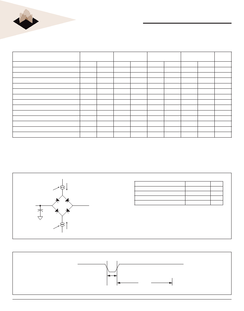
FIGURE 3 ≠ AC TEST CIRCUIT
Notes:
V
Z
is programmable from -2V to +7V.
I
OL
& I
OH
programmable from 0 to 16mA.
Tester Impedance Z0 = 75 ˝.
VZ is typically the midpoint of V
OH
and V
OL
.
I
OL
& I
OH
are adjusted to simulate a typical resistive load circuit.
ATE tester includes jig capacitance.
AC TEST CONDITIONS
Parameter
Typ
Unit
Input Pulse Levels
V
IL
= 0, V
IH
= 3.0
V
Input Rise and Fall
5
ns
Input and Output Reference Level
1.5
V
Output Timing Reference Level
1.5
V
Current Source
Current Source
I
OL
I
OH
C
eff
= 50 pf
D.U.T.
V
Z
1.5V
(Bipolar Supply)
AC CHARACTERISTICS ≠ WRITE/ERASE/PROGRAM OPERATIONS,CS# CONTROLLED
V
CC
= 5.0V, V
SS
= 0V, -55∞C T
A
+125∞C
Parameter
Symbol
-90
-120
-150
Unit
Min
Max
Min
Max
Min
Max
Write Cycle Time
t
AVAV
t
WC
90
120
150
ns
Write Enable Setup Time
t
WLEL
t
WS
0
0
0
ns
Chip Select Pulse Width
t
ELEH
t
CP
45
50
50
ns
Address Setup Time
t
AVEL
t
AS
0
0
0
ns
Data Setup Time
t
DVEH
t
DS
45
50
50
ns
Data Hold Time
t
EHDX
t
DH
0
0
0
ns
Address Hold Time
t
ELAX
t
AH
45
50
50
ns
Chip Select Pulse Width High
t
EHEL
t
CPH
20 20
20
ns
Duration of Byte Programming Operation (1)
t
WHWH1
300
300
300
µs
Sector Erase Time (2)
t
WHWH2
15
15
15
sec
Read Recovery Time
t
GHEL
0
0
0
µs
Chip Programming Time
44
44
44
sec
Chip Erase Time (3)
256
256
256
sec
Output Enable Hold Time (4)
t
OEH
10
10
10
ns
NOTES:
1.
Typical value for tWHWH1 is 7µs.
2.
Typical value for tWHWH2 is 1sec.
3.
Typical value for Chip Erase Time is 32sec.
4.
For Toggle and Data Polling.
FIGURE 4 ≠ RESET TIMING DIAGRAM
RESET#
t
RP
t
Ready
6
White Electronic Designs Corporation ∑ (602) 437-1520 ∑ www.wedc.com
White Electronic Designs
WF2M32-XXX5
October 2004
Rev. 5
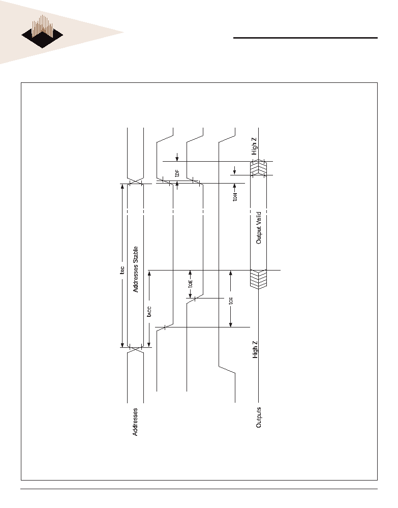
FIGURE 5 ≠ AC WAVEFORMS FOR READ OPERATIONS
CS#
OE#
WE#
7
White Electronic Designs Corporation ∑ (602) 437-1520 ∑ www.wedc.com
White Electronic Designs
WF2M32-XXX5
October 2004
Rev. 5
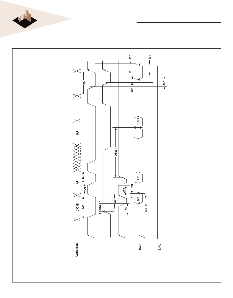
NOTES:
1.
PA is the address of the memory location to be programmed.
2.
PD is the data to be programmed at byte address.
3.
D7# is the output of the complement of the data written to each chip.
4. D
OUT
is the output of the data written to the device.
5.
Figure indicates last two bus cycles of four bus cycle sequence.
FIGURE 6 ≠ WRITE/ERASE/PROGRAM OPERATION, WE# CONTROLLED
CS#
Data# Polling
OE#
D
7
#
WE#
8
White Electronic Designs Corporation ∑ (602) 437-1520 ∑ www.wedc.com
White Electronic Designs
WF2M32-XXX5
October 2004
Rev. 5
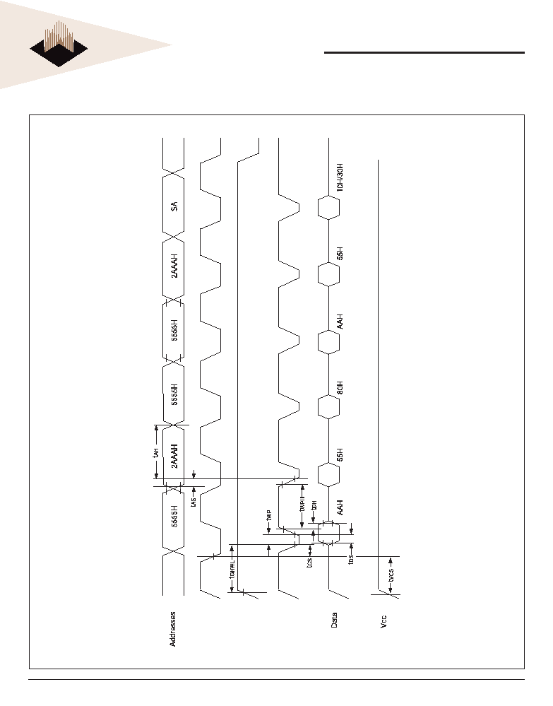
FIGURE 7 ≠ AC WAVEFORMS CHIP/SECTOR ERASE OPERATIONS
NOTE:
1. SA is the sector address for Sector Erase.
CS#
OE#
WE#

9
White Electronic Designs Corporation ∑ (602) 437-1520 ∑ www.wedc.com
White Electronic Designs
WF2M32-XXX5
October 2004
Rev. 5
FIGURE 8 ≠ AC WAVEFORMS FOR DATA# POLLING DURING EMBEDDED ALGORITHM
OPERATIONS
CS#
OE#
WE#
t
OE
t
CE
t
CH
t
OH
D7#
D7 =
V
a
lid Data
High Z
D0-D6 = Invalid
D0-D7
V
a
lid Data
t
DF
D7
D0-D6
t
OEH
t
WHWH 1 or 2
Data
10
White Electronic Designs Corporation ∑ (602) 437-1520 ∑ www.wedc.com
White Electronic Designs
WF2M32-XXX5
October 2004
Rev. 5
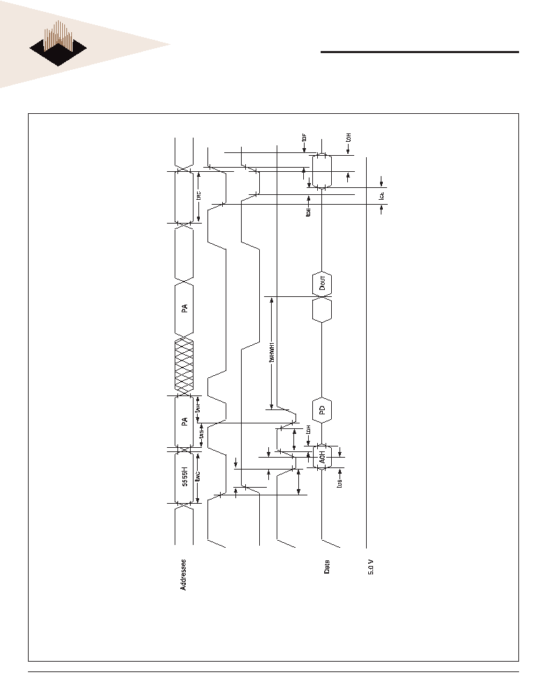
Notes:
1.
PA represents the address of the memory location to be programmed.
2.
PD represents the data to be programmed at byte address.
3.
D7# is the output of the complement of the data written to each chip.
4. D
OUT
is the output of the data written to the device.
5.
Figure indicates the last two bus cycles of a four bus cycle sequence.
FIGURE 9 ≠ ALTERNATE CS# CONTROLLED PROGRAMMING OPERATION TIMINGS
CS#
Data# Polling
OE#
D
7
#
WE#
t
GHEL
t
CP
t
WS
t
CPH
11
White Electronic Designs Corporation ∑ (602) 437-1520 ∑ www.wedc.com
White Electronic Designs
WF2M32-XXX5
October 2004
Rev. 5
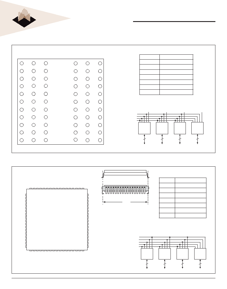
FIGURE 10 ≠ ALTERNATE PIN CONFIGURATION FOR WF2M32I-XHX5
PIN DESCRIPTION
I/O
0-31
Data Inputs/Outputs
A
0-20
Address Inputs
WE#
Write Enable
CS
1-4
#
Chip Selects
OE#
Output Enable
V
CC
Power Supply
GND
Ground
RESET#
Reset
TOP VIEW
BLOCK DIAGRAM
FIGURE 11 ≠ ALTERNATE PIN CONFIGURATION FOR WF2M32U-XG2UX5
BLOCK DIAGRAM
TOP VIEW
The WEDC 68 lead G2U CQFP fi lls the
same fi t and function as the JEDEC 68 lead
CQFJ or 68 PLCC. But the G2U has the
TCE and lead inspection advantage of the
CQFP form.
2M x 8
8
I/O
0-7
2M x 8
8
I/O
8-15
2M x 8
8
I/O
16-23
2M x 8
8
I/O
24-31
A
0-20
OE#
RESET#
CS#
WE#
10
11
12
13
14
15
16
17
18
19
20
21
22
23
24
25
26
60
59
58
57
56
55
54
53
52
51
50
49
48
47
46
45
44
9 8 7 6 5 4 3 2 1 68 67 66 65 64 63 62 61
27 28 29 30 31 32 33 34 35 36 37 38 39 40 41 42 43
I/O0
I/O1
I/O2
I/O3
I/O4
I/O5
I/O6
I/O7
GND
I/O8
I/O9
I/O10
I/O11
I/O12
I/O13
I/O14
I/O15
V
CC
A1
1
A12
A13
A14
A15
A16
CS#
OE#
NC
A17
NC
NC
NC
A18
A19
A20
I/O16
I/O17
I/O18
I/O19
I/O20
I/O21
I/O22
I/O23
GND
I/O24
I/O25
I/O26
I/O27
I/O28
I/O29
I/O30
I/O31
RESET#
A0
A1
A2
A3
A4
A5
NC
GND
NC
WE#
A6
A7
A8
A9
A10
V
CC
PIN DESCRIPTION
I/O
0-31
Data Inputs/Outputs
A
0-20
Address Inputs
WE#
Write Enable
CS#
Chip Select
OE#
Output Enable
V
CC
Power Supply
GND
Ground
RESET#
Reset
0.940"
I/O
8
I/O
9
I/O
10
A
14
A
16
A
11
A
0
A
18
I/O
0
I/O
1
I/O
2
RESET#
CS
2#
GND
I/O
11
A
10
A
9
A
15
V
CC
CS
1
#
A
19
I/O
3
I/O
15
I/O
14
I/O
13
I/O
12
OE#
A
17
WE#
I/O
7
I/O
6
I/O
5
I/O
4
I/O
24
I/O
25
I/O
26
A
7
A
12
NC
A
13
A
8
I/O
16
I/O
17
I/O
18
V
CC
CS
4
#
NC
I/O
27
A
4
A
5
A
6
A
20
CS
3
#
GND
I/O
19
I/O
31
I/O
30
I/O
29
I/O
28
A
1
A
2
A
3
I/O
23
I/O
22
I/O
21
I/O
20
11 22 33 44 55 66
1 12 23 34 45 56
2M x 8
8
I / O
0 - 7
CS1#
CS2#
CS3#
CS4#
2M x 8
8
I / O
8 - 1 5
2M x 8
8
I / O
1 6 - 2 3
2M x 8
8
I / O
2 4 - 3 1
A
0
-
20
OE#
WE#
RESET#
12
White Electronic Designs Corporation ∑ (602) 437-1520 ∑ www.wedc.com
White Electronic Designs
WF2M32-XXX5
October 2004
Rev. 5
FIGURE 12 ≠ PIN CONFIGURATION FOR WF2M32I-XG2UX5
PIN DESCRIPTION
I/O
0-31
Data Inputs/Outputs
A
0-20
Address Inputs
WE#
Write Enable
CS
1-4
#
Chip Selects
OE#
Output Enable
V
CC
Power Supply
GND
Ground
RESET#
Reset
TOP VIEW
BLOCK DIAGRAM
2M x 8
8
I / O
0 - 7
CS1#
CS2#
CS3#
CS4#
2M x 8
8
I / O
8 - 1 5
2M x 8
8
I / O
1 6 - 2 3
2M x 8
8
I / O
2 4 - 3 1
A
0
-
20
OE#
WE#
RESET#
The WEDC 68 lead G2U CQFP fi lls the same fi t and function as the
JEDEC 68 lead CQFJ or 68 PLCC. But the G2U has the TCE and lead
inspection advantage of the CQFP form.
0.940"
10
11
12
13
14
15
16
17
18
19
20
21
22
23
24
25
26
60
59
58
57
56
55
54
53
52
51
50
49
48
47
46
45
44
9 8 7 6 5 4 3 2 1 68 67 66 65 64 63 62 61
27 28 29 30 31 32 33 34 35 36 37 38 39 40 41 42 43
I/O0
I/O1
I/O2
I/O3
I/O4
I/O5
I/O6
I/O7
GND
I/O8
I/O9
I/O10
I/O11
I/O12
I/O13
I/O14
I/O15
V
CC
A1
1
A12
A13
A14
A15
A16
CS1#
OE#
CS2#
A17
NC
NC
NC
A18
A19
A20
I/O16
I/O17
I/O18
I/O19
I/O20
I/O21
I/O22
I/O23
GND
I/O24
I/O25
I/O26
I/O27
I/O28
I/O29
I/O30
I/O31
RESET#
A0
A1
A2
A3
A4
A5
CS3#
GND
CS4#
WE#
A6
A7
A8
A9
A10
V
CC
13
White Electronic Designs Corporation ∑ (602) 437-1520 ∑ www.wedc.com
White Electronic Designs
WF2M32-XXX5
October 2004
Rev. 5
30.1 (1.185) ± 0.38 (0.015) SQ
1.27 (0.050) ± 0.1 (0.005)
0.46 (0.018) ± 0.05 (0.002) DIA
1.27 (0.050) TYP DIA
0.76 (0.030) ± 0.1 (0.005)
25.4 (1.0) TYP
25.4 (1.0) TYP
15.24 (0.600) TYP
6.22 (0.245)
MAX
PIN 1 IDENTIFIER
SQUARE PAD
ON BOTTOM
3.81 (0.150)
±0.1 (0.005)
2.54 (0.100)
TYP
PACKAGE 401: 66 PIN, PGA TYPE, CERAMIC HEX-IN-LINE PACKAGE, HIP (H)
ALL LINEAR DIMENSIONS ARE MILLIMETERS AND PARENTHETICALLY IN INCHES
14
White Electronic Designs Corporation ∑ (602) 437-1520 ∑ www.wedc.com
White Electronic Designs
WF2M32-XXX5
October 2004
Rev. 5
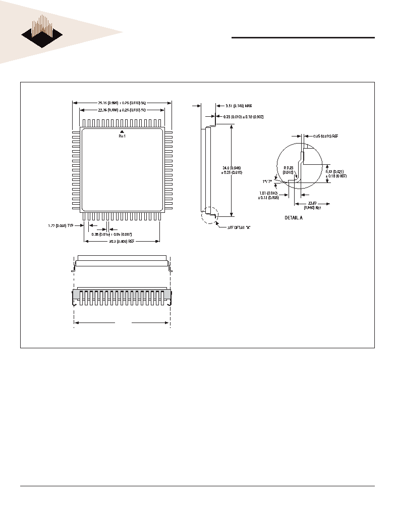
PACKAGE 510: 68 LEAD, CERAMIC QUAD FLAT PACK, CQFP (G2U)
ALL LINEAR DIMENSIONS ARE MILLIMETERS AND PARENTHETICALLY IN INCHES
0.940"
TYP
The WEDC 68 lead G2U CQFP fi lls the same
fi t and function as the JEDEC 68 lead CQFJ or
68 PLCC. But the G2U has the TCE and lead
inspection advantage of the CQFP form.

15
White Electronic Designs Corporation ∑ (602) 437-1520 ∑ www.wedc.com
White Electronic Designs
WF2M32-XXX5
October 2004
Rev. 5
LEAD FINISH:
Blank = Gold plated leads
A = Solder dip leads
V
PP
PROGRAMMING VOLTAGE
5 = 5 V
DEVICE
GRADE:
Q
=
Compliant
-55∞C
to
+125∞C
M
=
Military
-55∞C
to
+125∞C
I
= Industrial
-40∞C to +85∞C
C
=
Commercial
0∞C
to
+70∞C
PACKAGE TYPE:
H = Ceramic Hex In line Package, HIP (Package 401)
G2U = 22.4mm Ceramic Quad Flat Pack, CQFP (Package 510)
ACCESS
TIME
(ns)
IMPROVEMENT
MARK
∑ For HIP Package
Blank = 4CS# and 4WE#
I
=
4CS# and 1WE#, RESET#
∑ For G2U Package
Blank = 4CS# and 4WE#
U
=
1CS# and 1WE#
I
=
4CS# and 1WE#, RESET#
ORGANIZATION, 2M x 32
User confi gurable as 4M x 16 or 8M x 8
(Except WF2M32U-XG2UX which is 32 bit wide only.)
Flash
WHITE ELECTRONIC DESIGNS CORP.
ORDERING INFORMATION
W F 2M32 X - XXX X X 5 X