1
White Electronic Designs Corporation ∑ (602) 437-1520 ∑ www.whiteedc.com
HI-RELIABILITY PRODUCT
WF4M16-XDTX5
November 1999 Rev.3
2x2Mx16 5V FLASH MODULE
ADVANCED*
s Data Polling and Toggle Bit feature for detection of program
or erase cycle completion.
s Supports reading or programming data to a sector not being
erased.
s Built-in Decoupling Caps and Multiple Ground Pins for Low
Noise Operation, Separate Power and Ground Planes to
improve noise immunity
s RESET pin resets internal state machine to the read mode.
s Ready/Busy (RY/BY) output for direction of program or erase
cycle completion.
*
This data sheet describes a product that may or may not be under
development and is subject to change or cancellation without notice.
Note: For programming information refer to Flash Programming 16M5
Application Note.
FEATURES
s Access Time of 90, 120, 150ns
s Packaging:
∑ 56 Lead, Hermetic Ceramic, 0.520" CSOP (Package 213).
Fits standard 56 SSOP footprint.
s Sector Architecture
∑ 32 equal size sectors of 64KBytes per each 2Mx8 chip
∑ Any combination of sectors can be erased. Also supports
full chip erase.
s Minimum 100,000 Write/Erase Cycles Minimum
s Organized as two banks of 2Mx16; User Configurable as
4 x 2Mx8
s Commercial, Industrial, and Military Temperature Ranges
s 5 Volt Read and Write. 5V
±
10% Supply.
s Low Power CMOS
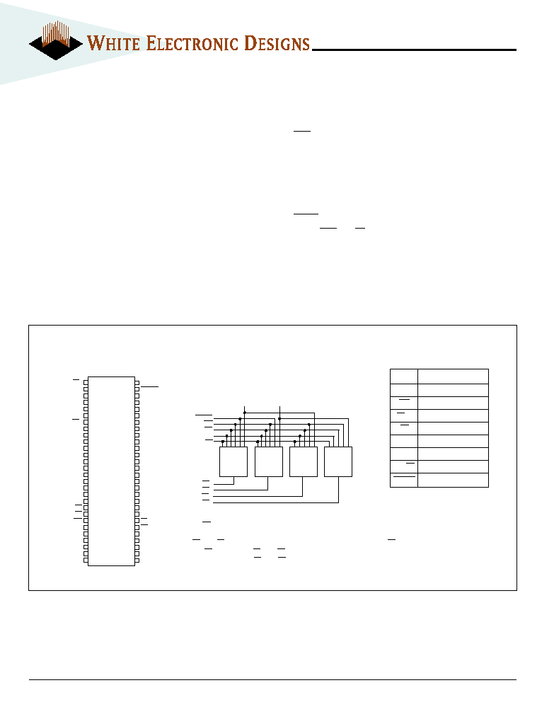
FIG. 1
PIN CONFIGURATION FOR WF4M16-XDTX5
BLOCK DIAGRAM
TOP VIEW
56 CSOP
PIN DESCRIPTION
I/O
0-15
Data Inputs/Outputs
A
0-20
Address Inputs
WE
Write Enable
CS
1-4
Chip Selects
OE
Output Enable
V
CC
Power Supply
GND
Ground
RY/BY
Ready/Busy
RESET
Reset
I / O
0 - 7
CS
1
I / O
8 - 1 5
CS
2
CS
3
CS
4
A
0 - 2 0
O E
W E
RY/BY
RESET
2M x 8
2M x 8
2M x 8
2M x 8
NOTE:
1. RY/BY is an open drain output and should be pulled-up to Vcc with an
external resistor.
2. CS
1
and CS
3
control the same data bus. Reads cannot be done with CS
1
and CS
3
both active. CS
2
and CS
4
control the same data bus. Reads
cannot be done with CS
2
and CS
4
both active.
3. Address compatible with Intel 2M8 56 SSOP.
1
2
3
4
5
6
7
8
9
10
11
12
13
14
15
16
17
18
19
20
21
22
23
24
25
26
27
28
56
55
54
53
52
51
50
49
48
47
46
45
44
43
42
41
40
39
38
37
36
35
34
33
32
31
30
29
CS1
A12
A13
A14
A15
NC
CS2
NC
A20
A19
A18
A17
A16
V
CC
GND
I/O6
I/O14
I/O7
I/O15
RY/BY
OE
WE
NC
I/O13
I/O5
I/O12
I/O4
V
CC
NC
RESET
A11
A10
A9
A1
A2
A3
A4
A5
A6
A7
GND
A8
V
CC
I/O9
I/O1
I/O8
I/O0
A0
NC
CS3
CS4
I/O2
I/O10
I/O3
I/O11
GND
2
White Electronic Designs Corporation ∑ (602) 437-1520 ∑ www.whiteedc.com
WF4M16-XDTX5
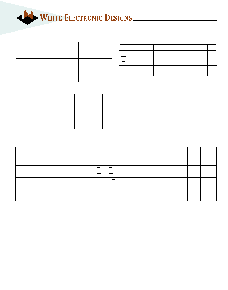
ABSOLUTE MAXIMUM RATINGS
Parameter
Symbol
Ratings
Unit
Voltage on Any Pin Relative to V
SS
V
T
-2.0 to +7.0
V
Power Dissipation
P
T
8
W
Storage Temperature
Tstg
-65 to +125
∞
C
Short Circuit Output Current
I
OS
100
mA
Endurance - Write/Erase Cycles
100,000 min
cycles
(Mil Temp)
Data Retention (Mil Temp)
20
years
RECOMMENDED DC OPERATING CONDITIONS
Parameter
Symbol
Min
Max
Unit
Supply Voltage
V
CC
4.5
5.5
V
Ground
V
SS
0
0
V
Input High Voltage
V
IH
2.0
V
CC
+ 0.5
V
Input Low Voltage
V
IL
-0.5
+0.8
V
Operating Temperature (Mil.)
T
A
-55
+125
∞
C
Operating Temperature (Ind.)
T
A
-40
+85
∞
C
DC CHARACTERISTICS - CMOS COMPATIBLE
(V
CC
= 5.0V, V
SS
= 0V, T
A
= -55
∞
C to +125
∞
C)
NOTES:
1. The Icc current listed includes both the DC operating current and the frequency dependent component (@ 5MHz). The frequency component typically is less than
2mA/MHz, with OE at V
IH
.
2. Icc active while Embedded Algorithm (program or erase) is in progress.
3. DC test conditions V
IL
= 0.3V, V
IH
= V
CC
- 0.3V
Parameter
Symbol
Conditions
Min
Max
Unit
Input Leakage Current
I
LI
V
CC
= 5.5, V
IN
= GND to V
CC
10
µ
A
Output Leakage Current
I
LOx32
V
CC
= 5.5, V
IN
= GND to V
CC
10
µ
A
V
CC
Active Current for Read (1)
I
CC1
CS = V
IL
, OE = V
IH
, f = 5MHz, V
CC
= 5.5
82
mA
V
CC
Active Current for Program or Erase (2)
I
CC2
CS = V
IL
, OE = V
IH
, V
CC
= 5.5
122
mA
V
CC
Standby Current
I
CC3
V
CC
= 5.5, CS = V
IH
, f = 5MHz
8.0
mA
Output Low Voltage
V
OL
I
OL
= 12.0 mA, V
CC
= 4.5
0.45
V
Output High Voltage
V
OH
I
OH
= -2.5 mA, V
CC
= 4.5
0.85xVcc
V
Low V
CC
Lock-Out Voltage
V
LKO
3.2
4.2
V
CAPACITANCE
(T
A
= +25
∞
C)
Parameter
Symbol
Conditions
Max
Unit
OE capacitance
C
OE
V
IN
= 0 V, f = 1.0 MHz
45
pF
WE capacitance
C
WE
V
IN
= 0 V, f = 1.0 MHz
45
pF
CS capacitance
C
CS
V
IN
= 0 V, f = 1.0 MHz
15
pF
Data I/O capacitance
C
I/O
V
I/O
= 0 V, f = 1.0 MHz
25
pF
Address input capacitance
C
AD
V
IN
= 0 V, f = 1.0 MHz
45
pF
This parameter is guaranteed by design but not tested.
3
White Electronic Designs Corporation ∑ (602) 437-1520 ∑ www.whiteedc.com
WF4M16-XDTX5
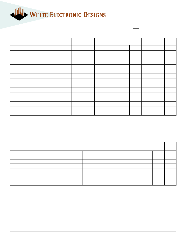
AC CHARACTERISTICS ≠ WRITE/ERASE/PROGRAM OPERATIONS - WE CONTROLLED
(V
CC
= 5.0V, T
A
= -55
∞
C to +125
∞
C)
Parameter
Symbol
-90
-120
-150
Unit
Min
Max
Min
Max
Min
Max
Write Cycle Time
t
AVAV
t
WC
90
120
150
ns
Chip Select Setup Time
t
ELWL
t
CS
0
0
0
ns
Write Enable Pulse Width
t
WLWH
t
WP
45
50
50
ns
Address Setup Time
t
AVWL
t
AS
0
0
0
ns
Data Setup Time
t
DVWH
t
DS
45
50
50
ns
Data Hold Time
t
WHDX
t
DH
0
0
0
ns
Address Hold Time
t
WLAX
t
AH
45
50
50
ns
Write Enable Pulse Width High
t
WHWL
t
WPH
20
20
20
ns
Duration of Byte Programming Operation (1)
t
WHWH1
300
300
300
µ
s
Sector Erase (2)
t
WHWH2
15
15
15
sec
Read Recovery Time before Write
t
GHWL
0
0
0
µ
s
V
CC
Setup Time
t
VCS
50
50
50
µ
s
Chip Programming Time
44
44
44
sec
Chip Erase Time (3)
256
256
256
sec
Output Enable Hold Time (4)
t
OEH
10
10
10
ns
NOTES:
1. Typical value for t
WHWH1
is 7
µ
s.
2. Typical value for t
WHWH2
is 1sec.
3. Typical value for Chip Erase Time is 32sec.
4. For Toggle and Data Polling.
AC CHARACTERISTICS ≠ READ-ONLY OPERATIONS
(V
CC
= 5.0V, T
A
= -55
∞
C to +125
∞
C)
Parameter
Symbol
-90
-120
-150
Unit
Min
Max
Min
Max
Min
Max
Read Cycle Time
t
AVAV
t
RC
90
120
150
ns
Address Access Time
t
AVQV
t
ACC
90
120
150
ns
Chip Select Access Time
t
ELQV
t
CE
90
120
150
ns
Output Enable to Output Valid
t
GLQV
t
OE
40
50
55
ns
Chip Select High to Output High Z (1)
t
EHQZ
t
DF
20
30
35
ns
Output Enable High to Output High Z (1)
t
GHQZ
t
DF
20
30
35
ns
Output Hold from Addresses, CS or OE Change,
t
AXQX
t
OH
0
0
0
ns
whichever is First
1. Guaranteed by design, not tested.
4
White Electronic Designs Corporation ∑ (602) 437-1520 ∑ www.whiteedc.com
WF4M16-XDTX5
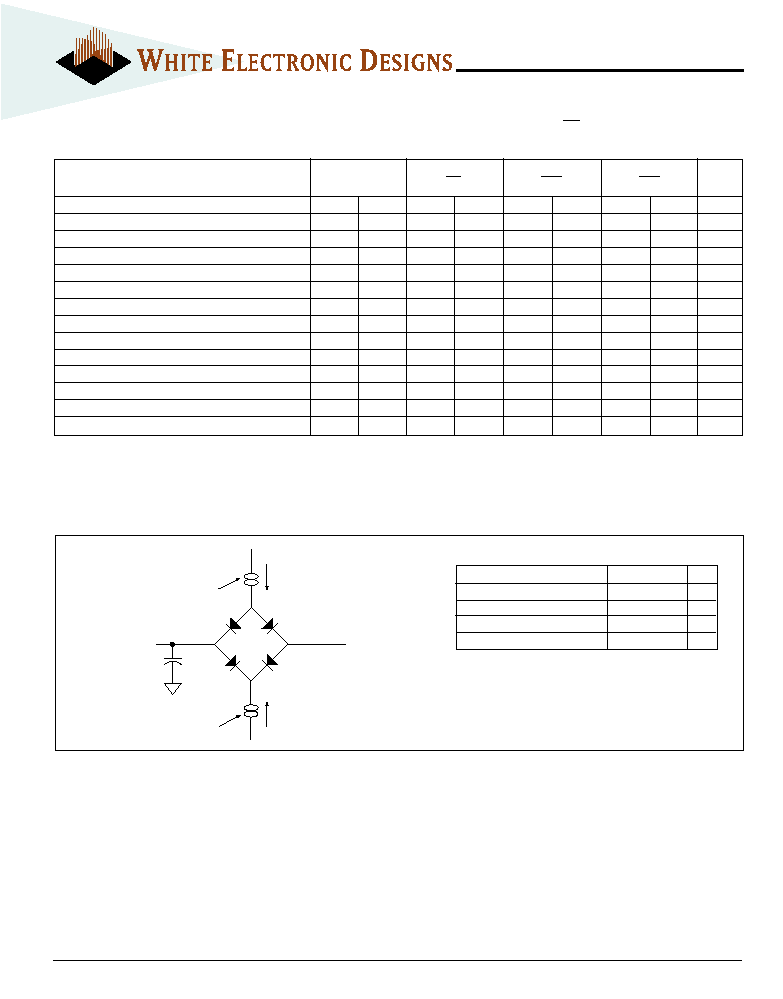
AC CHARACTERISTICS ≠ WRITE/ERASE/PROGRAM OPERATIONS,CS CONTROLLED
(V
CC
= 5.0V, V
SS
= 0V, T
A
= -55
∞
C to +125
∞
C)
FIG. 2
AC TEST CIRCUIT
AC TEST CONDITIONS
NOTES:
V
Z
is programmable from -2V to +7V.
I
OL
& I
OH
programmable from 0 to 16mA.
Tester Impedance Z
0
= 75
.
V
Z
is typically the midpoint of V
OH
and V
OL
.
I
OL
& I
OH
are adjusted to simulate a typical resistive load circuit.
ATE tester includes jig capacitance.
Parameter
Typ
Unit
Input Pulse Levels
V
IL
= 0, V
IH
= 3.0
V
Input Rise and Fall
5
ns
Input and Output Reference Level
1.5
V
Output Timing Reference Level
1.5
V
I
Current Source
D.U.T.
C = 50 pf
eff
I
OL
V
1.5V
(Bipolar Supply)
Z
Current Source
OH
Parameter
Symbol
-90
-120
-150
Unit
Min
Max
Min
Max
Min
Max
Write Cycle Time
t
AVAV
t
WC
90
120
150
ns
Write Enable Setup Time
t
WLEL
t
WS
0
0
0
ns
Chip Select Pulse Width
t
ELEH
t
CP
45
50
50
ns
Address Setup Time
t
AVEL
t
AS
0
0
0
ns
Data Setup Time
t
DVEH
t
DS
45
50
50
ns
Data Hold Time
t
EHDX
t
DH
0
0
0
ns
Address Hold Time
t
ELAX
t
AH
45
50
50
ns
Chip Select Pulse Width High
t
EHEL
t
CPH
20
20
20
ns
Duration of Byte Programming Operation (1)
t
WHWH1
300
300
300
µ
s
Sector Erase Time (2)
t
WHWH2
15
15
15
sec
Read Recovery Time
t
GHEL
0
0
0
µ
s
Chip Programming Time
44
44
44
sec
Chip Erase Time (3)
256
256
256
sec
Output Enable Hold Time (4)
t
OEH
10
10
10
ns
NOTES:
1. Typical value for t
WHWH1
is 7
µ
s.
2. Typical value for t
WHWH2
is 1sec.
3. Typical value for Chip Erase Time is 32sec.
4. For Toggle and Data Polling.
5
White Electronic Designs Corporation ∑ (602) 437-1520 ∑ www.whiteedc.com
WF4M16-XDTX5
FIG. 3
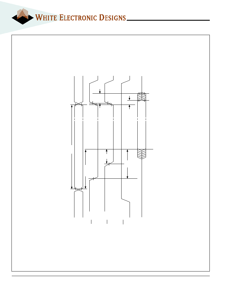
AC WAVEFORMS FOR READ OPERATIONS
Addresses
CS
OE
WE
Outputs
High Z
Addresses Stable
t
OE
t
RC
Output Valid
t
CE
t
ACC
t
OH
High Z
t
DF
6
White Electronic Designs Corporation ∑ (602) 437-1520 ∑ www.whiteedc.com
WF4M16-XDTX5
NOTES:
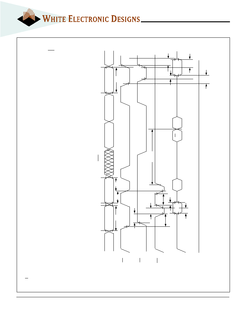
1. PA is the address of the memory location to be programmed.
2. PD is the data to be programmed at byte address.
3. D
7
is the output of the complement of the data written to each chip.
4. D
OUT
is the output of the data written to the device.
5. Figure indicates last two bus cycles of four bus cycle sequence.
FIG. 4
WRITE/ERASE/PROGRAM
OPERATION, WE CONTROLLED
Addresses
CS
OE
WE
Data
5.0 V
5555H
PA
PA
t
WC
t
CS
PD
D
7
D
OUT
t
AH
t
WPH
t
DH
t
DS
Data Polling
t
AS
t
RC
t
WP
A0H
t
OE
t
DF
t
OH
t
CE
t
GHWL
t
WHWH1
7
White Electronic Designs Corporation ∑ (602) 437-1520 ∑ www.whiteedc.com
WF4M16-XDTX5
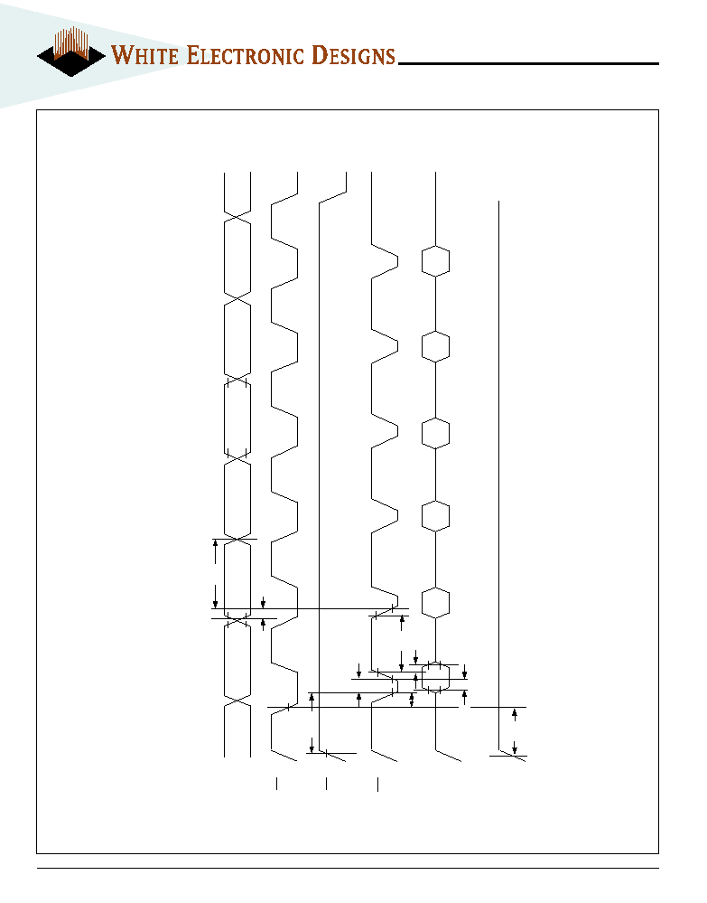
FIG. 5
AC WAVEFORMS CHIP/SECTOR
ERASE OPERATIONS
NOTE:
1. SA is the sector address for Sector Erase.
Addresses
CS
OE
WE
Data
V
CC
5555H
2AAAH
2AAAH
SA
5555H
5555H
t
WP
t
CS
t
VCS
10H/30H
55H
80H
55H
AAH
AAH
t
AH
t
GHWL
t
WPH
t
DH
t
DS
t
AS
8
White Electronic Designs Corporation ∑ (602) 437-1520 ∑ www.whiteedc.com
WF4M16-XDTX5
FIG. 6
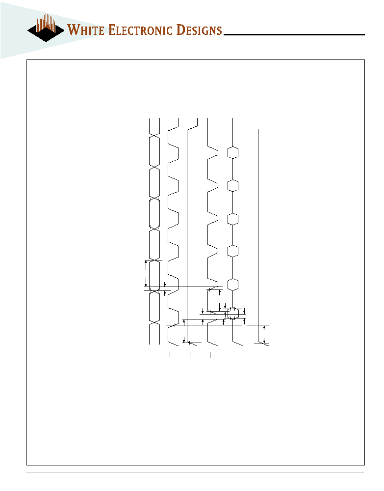
AC WAVEFORMS FOR DATA POLLING
DURING EMBEDDED ALGORITHM OPERATIONS
Addresses
CS
OE
WE
Data
V
CC
5555H
2AAAH
2AAAH
SA
5555H
5555H
t
WP
t
CS
t
VCS
10H/30H
55H
80H
55H
AAH
AAH
t
AH
t
GHWL
t
WPH
t
DH
t
DS
t
AS
9
White Electronic Designs Corporation ∑ (602) 437-1520 ∑ www.whiteedc.com
WF4M16-XDTX5
NOTES:
1. PA represents the address of the memory location to be programmed.
2. PD represents the data to be programmed at byte address.
3. D
7
is the output of the complement of the data written to each chip.
4. D
OUT
is the output of the data written to the device.
5. Figure indicates the last two bus cycles of a four bus cycle sequence.
Addresses
WE
OE
CS
Data
5.0 V
5555H
PA
PA
t
WC
t
WS
PD
D
7
D
OUT
t
AH
t
CPH
t
CP
t
DH
t
DS
Data Polling
t
AS
t
GHEL
A0H
t
WHWH1
FIG. 7
ALTERNATE CS CONTROLLED
PROGRAMMING OPERATION TIMINGS
10
White Electronic Designs Corporation ∑ (602) 437-1520 ∑ www.whiteedc.com
WF4M16-XDTX5
23.63 (0.930)
±
0.25 (0.010)
12.96 (0.510)
±
0.13 (0.005)
0.51
(0.020) TYP
0.51 (0.020)
±
0.13 (0.005)
0.18 (0.007)
±
0.03 (0.001)
21.59 (0.850) TYP
16.13 (0.635)
±
0.13 (0.005)
0.25 (0.010)
±
0.05 (0.002)
0.80 (0.031) TYP
10.93 (0.430)
±
0.13 (0.005)
4.57 (0.180)
MAX
PIN 1 IDENTIFIER
0
∞
/ -4
∞
1.58 (0.062) TYP
3.50 (0.138)
±
0.83 (0.032)
0.51 (0.020) TYP
+
DETAIL "A"
SEE DETAIL "A"
R 0.18
(0.007)
PACKAGE 213:
56 LEAD, DUAL CAVITY CERAMIC SOP
ALL LINEAR DIMENSIONS ARE MILLIMETERS AND PARENTHETICALLY IN INCHES
FIG. 8
ALTERNATE PIN CONFIGURATION FOR WF4M16W-XDTX5
BLOCK DIAGRAM
TOP VIEW
56 CSOP
PIN DESCRIPTION
I/O
0-15
Data Inputs/Outputs
A
0-20
Address Inputs
WE
Write Enable
CS
1-4
Chip Selects
OE
Output Enable
V
CC
Power Supply
GND
Ground
RY/BY
Ready/Busy
RESET
Reset
I / O
0 - 7
CS
1
I / O
8 - 1 5
CS
2
CS
3
CS
4
A
0 - 2 0
O E
W E
RY/BY
RESET
2M x 8
2M x 8
2M x 8
2M x 8
NOTE:
1. RY/BY is an open drain output and should be pulled-up to Vcc with an
external resistor.
2. CS
1
and CS
3
control the same data bus. Reads cannot be done with CS
1
and CS
3
both active. CS
2
and CS
4
control the same data bus. Reads
cannot be done with CS
2
and CS
4
both active.
3. Address compatible with Intel 1M16 56 SSOP, with the addition of
A20
at pin 8. Also refer to Note 2.
1
2
3
4
5
6
7
8
9
10
11
12
13
14
15
16
17
18
19
20
21
22
23
24
25
26
27
28
56
55
54
53
52
51
50
49
48
47
46
45
44
43
42
41
40
39
38
37
36
35
34
33
32
31
30
29
CS1
A11
A12
A13
A14
NC
CS2
A20
A19
A18
A17
A16
A15
V
CC
GND
I/O6
I/O14
I/O7
I/O15
RY/BY
OE
WE
NC
I/O13
I/O5
I/O12
I/O4
V
CC
NC
RESET
A10
A9
A8
A0
A1
A2
A3
A4
A5
A6
GND
A7
V
CC
I/O9
I/O1
I/O8
I/O0
NC
NC
CS3
CS4
I/O2
I/O10
I/O3
I/O11
GND
11
White Electronic Designs Corporation ∑ (602) 437-1520 ∑ www.whiteedc.com
WF4M16-XDTX5
ORDERING INFORMATION
LEAD FINISH:
Blank = Gold plated leads
A = Solder dip leads
V
PP
PROGRAMMING VOLTAGE
5 = 5 V
DEVICE GRADE:
M = Military, 883 Screened
-55
∞
C to +125
∞
C
I = Industrial
-40
∞
C to +85
∞
C
C = Commercial
0
∞
C to +70
∞
C
PACKAGE TYPE:
DT = 56 Lead Dual Cavity CSOP (Package 213)
fits standard 56 SSOP footprint
ACCESS TIME (ns)
ORGANIZATION, 2M x 16
User configurable as 4 x 2M x 8
Flash
WHITE ELECTRONIC DESIGNS CORP.
W F 4M16 - XXX DT X 5 X