1
White Electronic Designs Corporation ∑ Phoenix, AZ ∑ (602) 437-1520
HI-RELIABILITY PRODUCT
FEATURES
Access Times of 70, 90, 120, 150ns
Packaging
116 lead, 40mm square, Hermetic CQFP (Package 504)
100,000 Erase/Program Cycles Minimum
Sector Architecture
8 equal size sectors of 64KBytes each
Any combination of sectors can be concurrently erased.
Also supports full chip erase
Organized as 512Kx64, user configurable as 1Mx32, 2Mx16,
or 4Mx8.
Commercial, Industrial and Military Temperature Ranges
5 Volt Programming. 5V Ī 10% Supply.
Low Power CMOS, 6.5mA Standby
Embedded Erase and Program Algorithms
TTL Compatible Inputs and CMOS Outputs
Built-in Decoupling Caps for Low Noise Operation
Page Program Operation and Internal Program Control Time
Weight
WF512K64-XG4WX5 - 20 grams typical
* This data sheet describes a product under development, not fully character-
ized, and is subject to change without notice.
Note: Programming information available upon request.
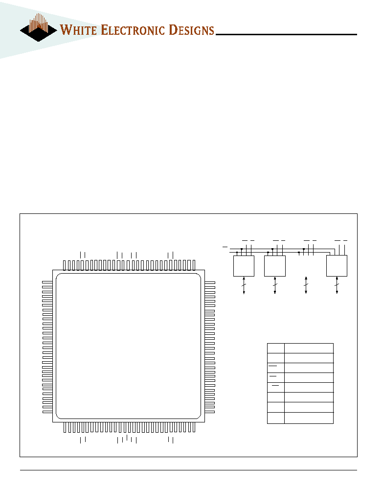
WF512K64-XG4WX5
FIG. 1
PIN CONFIGURATION FOR WF512K64-XG4WX5
1
512K x 8
8
I / O
0 - 7
CS
1
2
512K x 8
8
I / O
8 - 1 5
CS
2
8
I / O . . .
CS
x
8
512K x 8
8
I / O
5 6 - 6 3
CS
8
A
0 - 1 8
O E
WE
1
WE
2
WE
x
WE
8
. . . . . .
BLOCK DIAGRAM
16
17
18
19
20
21
22
23
24
25
26
27
28
29
30
31
32
33
34
35
36
37
38
39
40
41
42
43
44
15 14 13 12 11 10 9 8 7 6 5 4 3 2 1 116 115 114 113 112 111 110 109 108 107 106 105 104 103
I/O
3
I/O
4
I/O
5
I/O
6
I/O
7
GND
I/O
8
I/O
9
I/O
10
I/O
11
I/O
12
I/O
13
I/O
14
I/O
15
GND
I/O
16
I/O
17
I/O
18
I/O
19
I/O
20
I/O
21
I/O
22
I/O
23
GND
I/O
24
I/O
25
I/O
26
I/O
27
I/O
28
I/O
29
I/O
30
I/O
31
V
CC
WE
3
CS
3
NC NC A
18
A
17
A
16
A
15
WE
4
CS
4
OE CS
5
WE
5
A
14
A
13
A
12
A
11
A
10
NC CS
6
WE
6
V
CC
I/O
32
I/O
33
I/O
34
I/O
60
I/O
59
I/O
58
I/O
57
I/O
56
GND
I/O
55
I/O
54
I/O
53
I/O
52
I/O
51
I/O
50
I/O
49
I/O
48
GND
I/O
47
I/O
46
I/O
45
I/O
44
I/O
43
I/O
42
I/O
41
I/O
40
GND
I/O
39
I/O
38
I/O
37
I/O
36
I/O
35
I/O
2
I/O
1
I/O
0
V
CC
WE
2
CS
2
NC A
0
A
1
A
2
A
3
A
4
WE
1
CS
1
NC CS
8
WE
8
A
5
A
6
A
7
A
8
A
9
NC CS
7
WE
7
V
CC
I/O
63
I/O
62
I/O
61
45 46 47 48 49 50 51 52 53 54 55 56 57 58 59 60 61 62 63 64 65 66 67 68 69 70 71 72 73
102
101
100
99
98
97
96
95
94
93
92
91
90
89
88
87
86
85
84
83
82
81
80
79
78
77
76
75
74
TOP VIEW
I/O
0-63
Data Inputs/Outputs
A
0-18
Address Inputs
WE
1-8
Write Enables
CS
1-8
Chip Selects
OE
Output Enable
V
CC
Power Supply
GND
Ground
NC
Not Connected
PIN DESCRIPTION
512Kx64 5V FLASH MODULE
PRELIMINARY*
May 1999 Rev.2
2
White Electronic Designs Corporation ∑ Phoenix, AZ ∑ (602) 437-1520
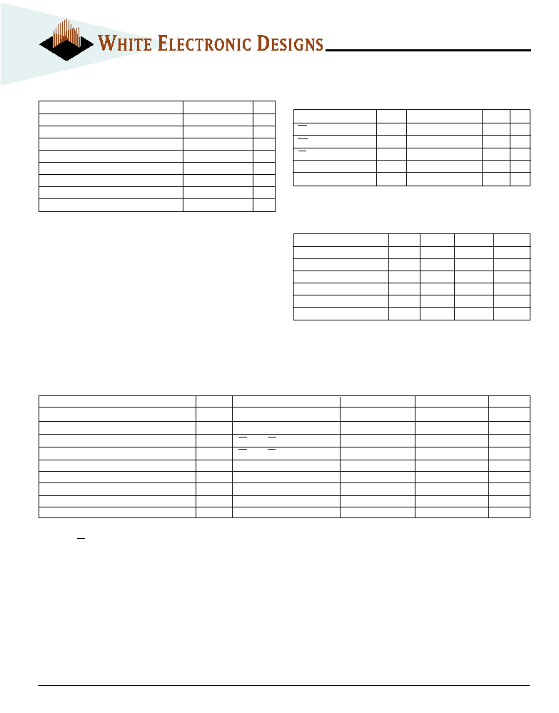
Parameter
Symbol
Conditions
Min
Max
Unit
Input Leakage Current
I
LI
V
CC
= 5.5, V
IN
= GND to V
CC
10
ĶA
Output Leakage Current
I
LOx32
V
CC
= 5.5, V
IN
= GND to V
CC
10
ĶA
V
CC
Active Current for Read (1)
I
CC1
CS = V
IL
, OE = V
IH
, f = 5MHz
380
mA
V
CC
Active Current for Program or Erase (2)
I
CC2
CS = V
IL
, OE = V
IH
480
mA
V
CC
Standby Current
I
CC4
V
CC
= 5.5, CS = V
IH
, f = 5MHz
13
mA
V
CC
Static Current
I
CC3
V
CC
= 5.5, CS = V
IH
1.2
mA
Output Low Voltage
V
OL
I
OL
= 8.0 mA, V
CC
= 4.5
0.45
V
Output High Voltage
V
OH1
I
OH
= -2.5 mA, V
CC
= 4.5
0.85
X
V
CC
V
Low V
CC
Lock-Out Voltage
V
LKO
3.2
4.2
V
WF512K64-XG4WX5
ABSOLUTE MAXIMUM RATINGS
NOTES:
1. Stresses above the absolute maximum rating may cause permanent damage
to the device. Extended operation at the maximum levels may degrade perfor-
mance and affect reliability.
2. Minimum DC voltage on input or I/O pins is -0.5V. During voltage transitions,
inputs may overshoot V
SS
to -2.0 V for periods of up to 20ns. Maximum DC
voltage on output and I/O pins is V
CC
+ 0.5V. During voltage transitions, outputs
may overshoot to Vcc + 2.0 V for periods of up to 20ns.
3. Minimum DC input voltage on A
9
pin is -0.5V. During voltage transitions, A
9
may overshoot Vss to -2V for periods of up to 20ns. Maximum DC input voltage
on A
9
is +13.5V which may overshoot to 14.0 V for periods up to 20ns.
DC CHARACTERISTICS - CMOS COMPATIBLE
(V
CC
= 5.0V, V
SS
= 0V, T
A
= -55įC to +125įC)
Parameter
Unit
Operating Temperature
-55 to +125
įC
Supply Voltage Range (V
CC
)
-2.0 to +7.0
V
Signal voltage range (any pin except A
9
) (2)
-2.0 to +7.0
V
Storage Temperature Range
-65 to +150
įC
Lead Temperature (soldering, 10 seconds)
+300
įC
Data Retention (Mil Temp)
20 years
Endurance (write/erase cycles) (Mil Temp)
100,000 cycles min.
A
9
Voltage for sector protect (V
ID
) (3)
-2.0 to +14.0
V
NOTES:
1. The I
CC
current listed includes both the DC operating current and the frequency dependent component (at 5 MHz). The frequency component typically is less than 2 mA/
MHz, with OE at V
IH
.
2. I
CC
active while Embedded Algorithm (program or erase) is in progress.
3. DC test conditions: V
IL
= 0.3V, V
IH
= V
CC
- 0.3V
RECOMMENDED OPERATING CONDITIONS
Parameter
Symbol
Min
Max
Unit
Supply Voltage
V
CC
4.5
5.5
V
Input High Voltage
V
IH
2.0
V
CC
+ 0.5
V
Input Low Voltage
V
IL
-0.5
+0.8
V
Operating Temp. (Mil.)
T
A
-55
+125
įC
Operating Temp. (Ind.)
T
A
-40
+85
įC
A
9
Voltage for Sector Protect
V
ID
11.5
12.5
V
CAPACITANCE
(T
A
= +25įC)
Parameter
Symbol
Conditions
Max
Unit
OE capacitance
C
OE
V
IN
= 0 V, f = 1.0 MHz
100
pF
WE capacitance
C
WE
V
IN
= 0 V, f = 1.0 MHz
20
pF
CS capacitance
C
CS
V
IN
= 0 V, f = 1.0 MHz
20
pF
Data I/O capacitance
C
I/O
V
I/O
= 0 V, f = 1.0 MHz
20
pF
Address input capacitance
C
AD
V
IN
= 0 V, f = 1.0 MHz
100
pF
This parameter is guaranteed by design but not tested.
3
White Electronic Designs Corporation ∑ Phoenix, AZ ∑ (602) 437-1520
WF512K64-XG4WX5
AC CHARACTERISTICS WRITE/ERASE/PROGRAM OPERATIONS,CS CONTROLLED
(V
CC
= 5.0V, V
SS
= 0V, T
A
= -55įC to +125įC)
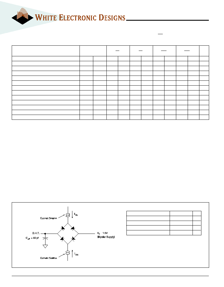
FIG. 2
AC TEST CIRCUIT
AC TEST CONDITIONS
NOTES:
V
Z
is programmable from -2V to +7V.
I
OL
& I
OH
programmable from 0 to 16mA.
Tester Impedance Z
0
= 75 ż.
V
Z
is typically the midpoint of V
OH
and V
OL
.
IOL & IOH
are adjusted to simulate a typical resistive load circuit.
ATE tester includes jig capacitance.
Parameter
Typ
Unit
Input Pulse Levels
V
IL
= 0, V
IH
= 3.0
V
Input Rise and Fall
5
ns
Input and Output Reference Level
1.5
V
Output Timing Reference Level
1.5
V
Parameter
Symbol
-70
-90
-120
-150
Unit
Min
Max
Min
Max
Min
Max
Write Cycle Time
t
AVAV
t
WC
70
90
120
150
ns
Write Enable Setup Time
t
WLEL
t
WS
0
0
0
0
ns
Chip Select Pulse Width
t
ELEH
t
CP
45
45
50
50
ns
Address Setup Time
t
AVEL
t
AS
0
0
0
0
ns
Data Setup Time
t
DVEH
t
DS
45
45
50
50
ns
Data Hold Time
t
EHDX
t
DH
0
0
0
0
ns
Address Hold Time
t
ELAX
t
AH
45
45
50
50
ns
Chip Select Pulse Width High
t
EHEL
t
CPH
20
20
20
20
ns
Duration of Byte Programming Operation (1)
t
WHWH1
300
300
300
300
Ķs
Chip and Sector Erase Time (2)
t
WHWH2
15
15
15
15
sec
Read Recovery Time
t
GHEL
0
0
0
0
ns
Chip Programming Time
11
11
11
11
sec
Chip Erase Time (3)
64
64
64
64
sec
NOTES:
1. Typical value for t
WHWH1
is 7Ķs.
2. Typical value for t
WHWH1
is 1sec.
3. Typical value for Chip Erase Time is 8sec.

4
White Electronic Designs Corporation ∑ Phoenix, AZ ∑ (602) 437-1520
AC CHARACTERISTICS WRITE/ERASE/PROGRAM OPERATIONS, WE CONTROLLED
(V
CC
= 5.0V, T
A
= -55įC to +125įC)
AC CHARACTERISTICS READ ONLY OPERATIONS
(V
CC
= 5.0V, T
A
= -55įC to +125įC)
Parameter
Symbol
-70
-90
-120
-150
Unit
Min
Max
Min
Max
Min
Max
Min
Max
Read Cycle Time
t
AVAV
t
RC
70
90
120
150
ns
Address Access Time
t
AVQV
t
ACC
70
90
120
150
ns
Chip Select Access Time
t
ELQV
t
CE
70
90
120
150
ns
Output Enable to Output Valid
t
GLQV
t
OE
35
35
50
55
ns
Chip Select to Output High Z (1)
t
EHQZ
t
DF
20
20
30
35
ns
Output Enable High to Output High Z (1)
t
GHQZ
t
DF
20
20
30
35
ns
Output Hold from Address, CS or OE Change,
t
AXQX
t
OH
0
0
0
0
ns
whichever is First
1. Guaranteed by design, but not tested
Parameter
Symbol
-70
-90
-120
-150
Unit
Min
Max
Min
Max
Min
Max
Min
Max
Write Cycle Time
t
AVAV
t
WC
70
90
120
150
ns
Chip Select Setup Time
t
ELWL
t
CS
0
0
0
0
ns
Write Enable Pulse Width
t
WLWH
t
WP
45
45
50
50
ns
Address Setup Time
t
AVWH
t
AS
0
0
0
0
ns
Data Setup Time
t
DVWH
t
DS
45
45
50
50
ns
Data Hold Time
t
WHDX
t
DH
0
0
0
0
ns
Address Hold Time
t
WHAX
t
AH
45
45
50
50
ns
Write Enable Pulse Width High
t
WHWL
t
WPH
20
20
20
20
ns
Duration of Byte Programming Operation (1)
t
WHWH1
300
300
300
300
Ķs
Sector Erase Time (2)
t
WHWH2
15
15
15
15
sec
Read Recovery Time before Write
t
GHWL
0
0
0
0
ns
V
CC
Set-up Time
t
VCS
50
50
50
50
Ķs
Chip Programming Time
11
11
11
11
sec
Output Enable Setup Time
t
OES
0
0
0
0
ns
Output Enable Hold Time (4)
t
OEH
10
10
10
10
ns
Chip Erase Time (3)
64
64
64
64
sec
NOTES:
1. Typical value for t
WHWH1
is 7Ķs.
2. Typical value for t
WHWH1
is 1sec.
3. Typical value for Chip Erase Time is 8sec.
4. For Toggle and Data Polling.
WF512K64-XG4WX5
5
White Electronic Designs Corporation ∑ Phoenix, AZ ∑ (602) 437-1520
FIG. 3
AC WAVEFORMS FOR READ OPERATIONS
Addresses
CS
OE
WE
Outputs
High Z
Addresses Stable
t
OE
t
RC
Output Valid
t
CE
t
ACC
t
OH
High Z
t
DF
WF512K64-XG4WX5
6
White Electronic Designs Corporation ∑ Phoenix, AZ ∑ (602) 437-1520
NOTES:
1. PA is the address of the memory location to be programmed.
2. PD is the data to be programmed at byte address.
3. D
7
is the output of the complement of the data written to each chip.
4. D
OUT
is the output of the data written to the device.
5. Figure indicates last two bus cycles of four bus cycle sequence.
FIG. 4
WRITE/ERASE/PROGRAM
OPERATION, WE CONTROLLED
Addresses
CS
OE
WE
Data
5.0 V
5555H
PA
PA
t
WC
t
CS
PD
D
7
D
OUT
t
AH
t
WPH
t
DH
t
DS
Data Polling
t
AS
t
RC
t
WP
A0H
t
OE
t
DF
t
OH
t
CE
t
GHWL
t
WHWH1
WF512K64-XG4WX5
7
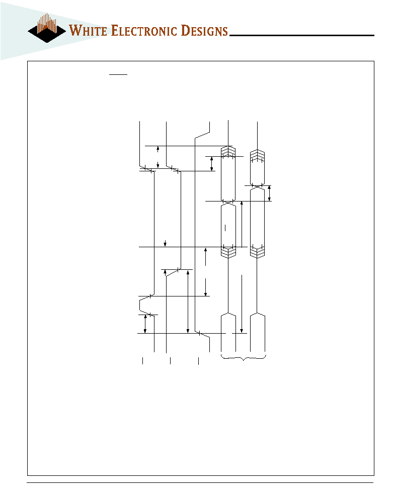
White Electronic Designs Corporation ∑ Phoenix, AZ ∑ (602) 437-1520
NOTE:
1. SA is the sector address for Sector Erase.
Addresses
CS
OE
WE
Data
V
CC
5555H
2AAAH
2AAAH
SA
5555H
5555H
t
WP
t
CS
t
VCS
10H/30H
55H
80H
55H
AAH
AAH
t
AH
t
AS
t
GHWL
t
WPH
t
DH
t
DS
FIG. 5
AC WAVEFORMS CHIP/SECTOR
ERASE OPERATIONS
WF512K64-XG4WX5
8
White Electronic Designs Corporation ∑ Phoenix, AZ ∑ (602) 437-1520
FIG. 6
AC WAVEFORMS FOR DATA POLLING
DURING EMBEDDED ALGORITHM OPERATIONS
CS
OE
WE
t
OE
t
CE
t
CH
t
OH
D7
D7 =
Valid Data
High Z
D0-D6 = Invalid
D0-D7
Valid Data
t
DF
D7
D0-D6
t
OEH
t
WHWH 1 or 2
t
OE
Data
WF512K64-XG4WX5
9
White Electronic Designs Corporation ∑ Phoenix, AZ ∑ (602) 437-1520
Notes:
1. PA represents the address of the memory location to be programmed.
2. PD represents the data to be programmed at byte address.
3. D
7
is the output of the complement of the data written to each chip.
4. D
OUT
is the output of the data written to the device.
5. Figure indicates the last two bus cycles of a four bus cycle sequence.
Addresses
WE
OE
CS
Data
5.0 V
5555H
PA
PA
t
WC
t
WS
PD
D
7
D
OUT
t
AH
t
CPH
t
CP
t
DH
t
DS
Data Polling
t
AS
t
GHEL
A0H
t
WHWH1
FIG. 7
ALTERNATE CS CONTROLLED
PROGRAMMING OPERATION TIMINGS
WF512K64-XG4WX5

1 0
White Electronic Designs Corporation ∑ Phoenix, AZ ∑ (602) 437-1520
V
PP
PROGRAMMING VOLTAGE
5 = 5V
DEVICE GRADE:
M = Military Screened
-55įC to +125įC
I = Industrial
-40įC to +85įC
C = Commercial
0įC to + 70įC
PACKAGE TYPE:
G4W = 116 Lead 40mm Ceramic Quad Flat Pack, CQFP (Package 504)
ACCESS TIME (ns)
ORGANIZATION, 512K x 64
User configurable as 1M x 32, 2M x 16 or 4M x 8
Flash
WHITE ELECTRONIC DESIGNS CORP.
ORDERING INFORMATION
PACKAGE 504:
116 LEAD, CERAMIC QUAD FLAT PACK, CQFP (G4W)
ALL LINEAR DIMENSIONS ARE MILLIMETERS AND PARENTHETICALLY IN INCHES
38 (1.50) REF
4 PLACES
0.38 (0.015)
Ī 0.08 (0.003)
68 PLACES
1.27 (0.050)
REF
5.1 (0.200)
Ī 0.25 (0.010)
4 PLACES
39.6 (1.56) Ī 0.38 (0.015) SQ
12.7 (0.500)
Ī 0.5 (0.020)
4 PLACES
5.1 (0.200) MAX
0.25 (0.010)
Ī 0.05 (0.002)
1.27 (0.050)
Ī 0.1 (0.005)
PIN 1 IDENTIFIER
Pin 1
W F 512K64 - XXX G4W X 5
WF512K64-XG4WX5