1
White Electronic Designs Corporation ∑ (602) 437-1520 ∑ www.wedc.com
White Electronic Designs
WF8M32-XG4DX5
October 1999
Rev. 3
ADVANCED*
White Electronic Designs Corp. reserves the right to change products or specifi cations without notice.
8Mx32 5V FLASH MODULE
FEATURES
Access Time of 100, 120, 150ns
Packaging:
∑ 68 Lead, 40 mm (1.560") square hermetic CQFP,
5.2 mm (0.205") high (Package 503)
Sector
Architecture
∑ 32 equal size sectors of 64KBytes per each 2Mx8
chip
∑ Any combination of sectors can be erased. Also
supports full chip erase.
100,000 Write/Erase Cycles Minimum
Organized
as
8Mx32
Commercial,
Industrial,
and
Military
Temperature
Ranges
5 Volt Read and Write. 5V Ī 10% Supply.
Low
Power
CMOS
Data# Polling and Toggle Bit feature for detection of
program or erase cycle completion.
Supports reading or programming data to a sector
not being erased.
RESET# pin resets internal state machine to the
read mode. (Not available in HIP package for
WF2M32-XHX5)
Built-in Decoupling Caps and Multiple Ground Pins
for Low Noise Operation, Seperate Power and
Ground Planes to improve noise immunity.
Built
in
Buffering.
* This product is under development, is not qualifi ed or characterized and is subject to
change or cancellation without notice.
Note: For programming information refer to Flash Programming 16M5 Application Note.
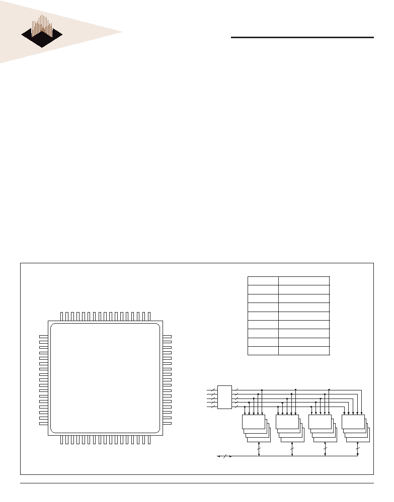
PIN DESCRIPTION
I/O0-31
Data Inputs/Outputs
A0-22
Address Inputs
WE
Write Enable
CS1-4
Chip Selects
OE
Output Enable
VCC
Power Supply
RESET
Reset
GND
Ground
NC Not
Connected
FIGURE 1 ≠ PIN CONFIGURATIONFOR
WF8M32-XG4DX5
10
11
12
13
14
15
16
17
18
19
20
21
22
23
24
25
26
60
59
58
57
56
55
54
53
52
51
50
49
48
47
46
45
44
9 8 7 6 5 4 3 2 1 68 67 66 65 64 63 62 61
27 28 29 30 31 32 33 34 35 36 37 38 39 40 41 42 43
I/O0
I/O1
I/O2
I/O3
I/O4
I/O5
I/O6
I/O7
GND
I/O8
I/O9
I/O10
I/O11
I/O12
I/O13
I/O14
I/O15
VCC
A1
1
A12
A13
A14
A15
A16
CS2#
OE#
CS4#
A17
A18
A19
A20
A21
RESET#
A22
I/O16
I/O17
I/O18
I/O19
I/O20
I/O21
I/O22
I/O23
GND
I/O24
I/O25
I/O26
I/O27
I/O28
I/O29
I/O30
I/O31
NC
A0
A1
A2
A3
A4
A5
CS1#
GND
CS3#
WE#
A6
A7
A8
A9
A10
VCC
BLOCK DIAGRAM
Top View
2M x 8
2M x 8
2M x 8
2M x 8
2M x 8
2M x 8
2M x 8
2M x 8
2M x 8
2M x 8
2M x 8
2M x 8
2M x 8
2M x 8
2M x 8
2M x 8
I/O0-31
Interface
1
4
1
1
23
1
4
1
1
23
CS1#
8
I / O
0 - 7
8
I / O
8 - 1 5
8
I / O
1 6 - 2 3
8
I / O
2 4 - 3 1
CS2#
CS3#
CS4#
32
RESET#
CS1-4#
WE#
OE#
A0-22
CS1# selects I/O0-7, CS2# selects I/O8-15, CS3# selects I/O16-23, CS4# selects I/O24-31
2
White Electronic Designs Corporation ∑ (602) 437-1520 ∑ www.wedc.com
White Electronic Designs
WF8M32-XG4DX5
October 1999
Rev. 3
ADVANCED
White Electronic Designs Corp. reserves the right to change products or specifi cations without notice.
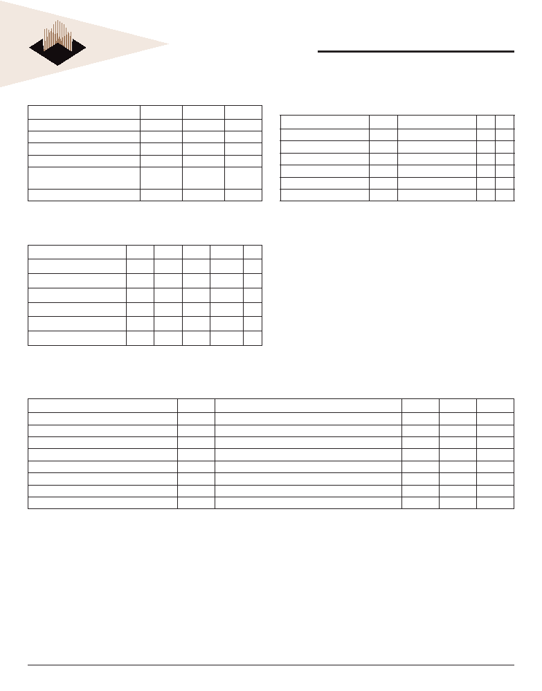
CAPACITANCE
T
A
= +25įC
Parameter
Symbol
Conditions Max Unit
OE# capacitance
C
OE
V
IN
= 0 V, f = 1.0 MHz
20
pF
WE# capacitance
C
WE
V
IN
= 0 V, f = 1.0 MHz
20
pF
CS1-4# capacitance
C
CS
V
IN
= 0 V, f = 1.0 MHz
20
pF
Data I/O capacitance
C
I/O
V
I/O
= 0 V, f = 1.0 MHz
60
pF
Address input capacitance
C
AD
V
IN
= 0 V, f = 1.0 MHz
20
pF
RESET# capacitance
C
RST
V
IN
= 0 V, f = 1.0 MHz
20
pF
This parameter is guaranteed by design but not tested.
ABSOLUTE MAXIMUM RATINGS
Parameter
Symbol
Ratings
Unit
Voltage on Any Pin Relative to V
SS
V
T
-2.0 to +7.0
V
Power Dissipation
P
T
8
W
Storage Temperature
T
STG
-65 to +125
įC
Short Circuit Output Current
I
OS
100
mA
Endurance - Write/Erase Cycles
(Mil Temp)
100,000 min
cycles
Data Retention (Mil Temp)
20
years
RECOMMENDED DC OPERATING CONDITIONS
Parameter
Symbol
Min
Typ
Max
Unit
Supply Voltage
V
CC
4.5
5.0
5.5
V
Ground
V
SS
0
0
0
V
Input High Voltage
V
IH
2.0
--
V
CC
+ 0.5
V
Input Low Voltage
V
IL
-0.5
--
+0.8
V
Operating Temperature (Mil.)
T
A
-55
--
+125
įC
Operating Temperature (Ind.)
T
A
-40
--
+85
įC
DC CHARACTERISTICS ≠ CMOS COMPATIBLE
V
CC
= 5.0V, GND = 0V, -55įC T
A
+125įC
Parameter
Symbol
Conditions
Min
Max
Unit
Input Leakage Current
I
LI
V
CC
= 5.5, V
IN
= GND to V
CC
10
ĶA
Output Leakage Current
I
LOx32
V
CC
= 5.5, V
IN
= GND to V
CC
10
ĶA
V
CC
Active Current for Read (1)
I
CC1
CS# = V
IL
, OE# = V
IH
, f = 5MHz
640
mA
V
CC
Active Current for Program or Erase (2)
I
CC2
CS# = V
IL
, OE# = V
IH
960
mA
V
CC
Standby Current
I
CC3
V
CC
= 5.5, CS# = V
IH
, f = 5MHz, RESET# = V
CC
Ī 0.3V
160
mA
Output Low Voltage
V
OL
I
OL
= 12.0 mA, V
CC
= 4.5
0.45
V
Output High Voltage
V
OH
I
OH
= -2.5 mA, V
CC
= 4.5
0.85 x V
CC
V
Low V
CC
Lock-Out Voltage
V
LKO
3.2
4.2
V
Notes:
1. The Icc current listed includes both the DC operating current and the frequency dependent component (@ 5MHz).
The frequency component typically is less than 2mA/MHz, with OE# at V
IH
.
2. I
CC
active while Embedded Algorithm (program or erase) is in progress.
3. DC test conditions V
IL
= 0.3V, V
IH
= V
CC
- 0.3V
3
White Electronic Designs Corporation ∑ (602) 437-1520 ∑ www.wedc.com
White Electronic Designs
WF8M32-XG4DX5
October 1999
Rev. 3
ADVANCED
White Electronic Designs Corp. reserves the right to change products or specifi cations without notice.
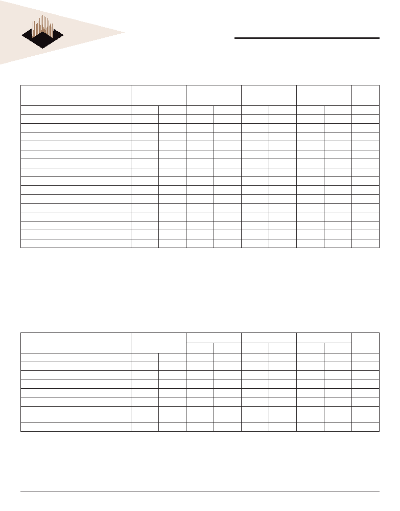
AC CHARACTERISTICS ≠ WRITE/ERASE/PROGRAM OPERATIONS ≠ WE# CONTROLLED
V
CC
= 5.0V, -55įC T
A
+125įC
Parameter
Symbol
-100
-120
-150
Unit
Min
Max
Min
Max
Min
Max
Write Cycle Time
t
AVAV
t
WC
100
120
150
ns
Chip Select Setup Time
t
ELWL
t
CS
0
0
0
ns
Write Enable Pulse Width
t
WLWH
t
WP
50
50
50
ns
Address Setup Time
t
AVWL
t
AS
0
0
0
ns
Data Setup Time
t
DVWH
t
DS
50
50
50
ns
Data Hold Time
t
WHDX
t
DH
0
0
0
ns
Address Hold Time
t
WLAX
t
AH
50
50
50
ns
Write Enable Pulse Width High
t
WHWL
t
WPH
20
20
20
ns
Duration of Byte Programming Operation (1)
t
WHWH1
300
300
300
Ķs
Sector Erase (2)
t
WHWH2
15
15
15
sec
Read Recovery Time before Write
t
GHWL
0
0
0
Ķs
V
CC
Setup Time
t
VCS
50
50
50
Ķs
Chip Programming Time
44
44
44
sec
Chip Erase Time (3)
256
256
256
ns
Output Enable Hold Time (4)
t
OEH
10
10
10
ns
RESET# Pulse Width
t
RP
500
500
500
ns
NOTES:
1. Typical value for t
WHWH1
is 7Ķs.
2. Typical value for t
WHWH2
is 1sec.
3. Typical value for Chip Erase Time is 32sec.
4. For Toggle and Data Polling.
AC CHARACTERISTICS ≠ READ-ONLY OPERATIONS
V
CC
= 5.0V, -55įC T
A
+125įC
Parameter
Symbol
-100
-120
-150
Unit
Min
Max
Min
Max
Min
Max
Read Cycle Time
t
AVAV
t
RC
100
120
150
ns
Address Access Time
t
AVQV
t
ACC
100
120
150
ns
Chip Select Access Time
t
ELQV
t
CE
100
120
150
ns
Output Enable to Output Valid
t
GLQV
t
OE
50
50
55
ns
Chip Select High to Output High Z (1)
t
EHQZ
t
DF
30
30
35
ns
Output Enable High to Output High Z (1)
t
GHQZ
t
DF
30
30
35
ns
Output Hold from Addresses, CS# or OE#
Change, whichever is First
t
AXQX
t
OH
0
0
0
ns
RST Low to Read Mode (1)
tReady
20
20
20
Ķs
1. Guaranteed by design, not tested.

4
White Electronic Designs Corporation ∑ (602) 437-1520 ∑ www.wedc.com
White Electronic Designs
WF8M32-XG4DX5
October 1999
Rev. 3
ADVANCED
White Electronic Designs Corp. reserves the right to change products or specifi cations without notice.
FIGURE 3 ≠ RESET TIMING DIAGRAM
AC CHARACTERISTICS ≠ WRITE/ERASE/PROGRAM OPERATIONS ≠ CS# CONTROLLED
V
CC
= 3.3V, V
SS
= 0V, -55įC T
A
+125įC
Parameter
Symbol
-100
-120
-150
Unit
Min
Max
Min
Max
Min
Max
Write Cycle Time
t
AVAV
t
WC
100
120
150
ns
Write Enable Setup Time
t
WLEL
t
WS
0
0
0
ns
Chip Select Pulse Width
t
ELEH
t
CP
50
50
50
ns
Address Setup Time
t
AVEL
t
AS
0
0
0
ns
Data Setup Time
t
DVEH
t
DS
50
50
50
ns
Data Hold Time
t
EHDX
t
DH
0
0
0
ns
Address Hold Time
t
ELAX
t
AH
50
50
50
ns
Chip Select Pulse Width High
t
EHEL
t
CPH
20
20
20
ns
Duration of Byte Programming Operation (1)
t
WHWH1
300
300
300
Ķs
Sector Erase Time (2)
t
WHWH2
15
15
15
sec
Read Recovery Time (2)
t
GHEL
0
0
0
Ķs
Chip Programming Time
100
100
100
sec
Chip Erase Time (3)
480
480
480
sec
Output Enable Hold Time (4)
t
OEH
10
10
10
ns
NOTES:
1. Typical value for tWHWH1 is 7Ķs.
2. Typical value for tWHWH2 is 1sec.
3. Typical value for Chip Erase Time is 32sec.
4. For Toggle and Data Polling.
FIGURE 2 ≠ AC TEST CIRCUIT
AC TEST CONDITIONS
Parameter
Typ
Unit
Input Pulse Levels
V
IL
= 0, V
IH
= 3.0
V
Input Rise and Fall
5
ns
Input and Output Reference Level
1.5
V
Output Timing Reference Level
1.5
V
NOTES:
V
Z
is programmable from -2V to +7V.
I
OL
& I
OH
programmable from 0 to 16mA.
Tester Impedance Z0 = 75 .
V
Z
is typically the midpoint of V
OH
and V
OL
.
I
OL
& I
OH
are adjusted to simulate a typical resistive load circuit.
ATE tester includes jig capacitance.
I
Current Source
D.U.T.
C = 50 pf
eff
I
OL
V
1.5V
(Bipolar Supply)
Z
Current Source
OH
RESET#
t
RP
t
Ready

5
White Electronic Designs Corporation ∑ (602) 437-1520 ∑ www.wedc.com
White Electronic Designs
WF8M32-XG4DX5
October 1999
Rev. 3
ADVANCED
White Electronic Designs Corp. reserves the right to change products or specifi cations without notice.
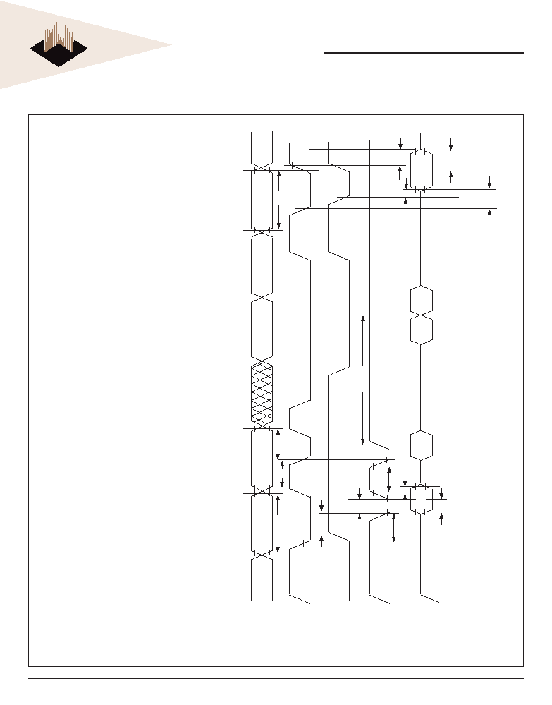
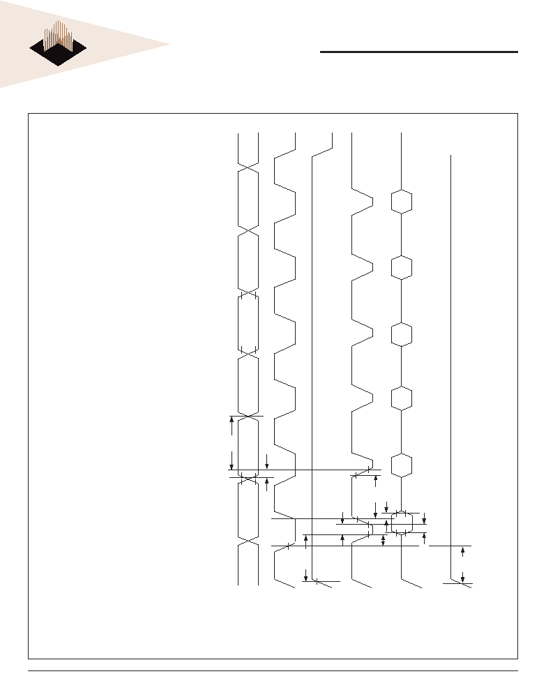
FIGURE 4 ≠ AC WAVEFORMS FOR READ OPERATIONS
s
e
s
s
e
r
d
d
A
CS#
OE#
WE#
s
t
u
p
t
u
O
Z
h
g
i
H
e
l
b
a
t
S
s
e
s
s
e
r
d
d
A
t
E
O
t
C
R
d
i
l
a
V
t
u
p
t
u
O
t
E
C
t
C
C
A
t
H
O
Z
h
g
i
H
t
F
D
6
White Electronic Designs Corporation ∑ (602) 437-1520 ∑ www.wedc.com
White Electronic Designs
WF8M32-XG4DX5
October 1999
Rev. 3
ADVANCED
White Electronic Designs Corp. reserves the right to change products or specifi cations without notice.
NOTES:
1. PA is the address of the memory location to be programmed.
2. PD is the data to be programmed at byte address.
3. D7# is the output of the complement of the data written to each chip.
4. D
OUT
is the output of the data written to the device.
5. Figure indicates last two bus cycles of four bus cycle sequence.
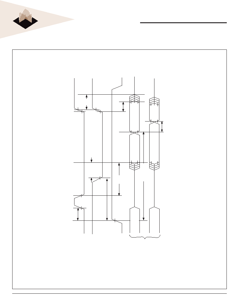
WRITE/ERASE/PROGRAM OPERATION, WE# CONTROLLED
s
e
s
s
e
r
d
d
A
CS#
E#
O
E#
W
a
t
a
D
V
0
.
5
A
P
A
P
H
5
5
5
5
t
C
W
t
S
C
D
P
D#
7
D
T
U
O
t
H
A
t
H
P
W
t
H
D
t
S
D
Data# Polling
t
S
A
t
C
R
t
P
W
H
0
A
0
A
t
E
O
t
F
D
t
H
O
t
E
C
t
L
W
H
G
t
1
H
W
H
W
7
White Electronic Designs Corporation ∑ (602) 437-1520 ∑ www.wedc.com
White Electronic Designs
WF8M32-XG4DX5
October 1999
Rev. 3
ADVANCED
White Electronic Designs Corp. reserves the right to change products or specifi cations without notice.
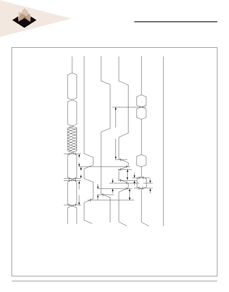
AC WAVEFORMS CHIP/SECTOR ERASE OPERATIONS
NOTE:
1. SA is the sector address for Sector Erase.
Addresses
CS#
OE#
WE#
Data
V
CC
5555H
2AAAH
2AAAH
SA
5555H
5555H
t
WP
t
CS
t
VCS
1010H/3030H
5555H
8080H
5555H
AAAAH
AAAAH
t
AH
t
AS
t
GHWL
t
WPH
t
DH
t
DS
8
White Electronic Designs Corporation ∑ (602) 437-1520 ∑ www.wedc.com
White Electronic Designs
WF8M32-XG4DX5
October 1999
Rev. 3
ADVANCED
White Electronic Designs Corp. reserves the right to change products or specifi cations without notice.
AC WAVEFORMS FOR DATA# POLLING DURING EMBEDDED ALGORITHM OPERATIONS
S#
C
E#
O
E#
W
t
E
O
t
E
O
t
E
C
t
H
C
t
H
O
O#
#
/
I
7
O
/
I
d
n
a
5
1
O
/
I
7
O
/
I
d
n
a
5
1
a
t
a
D
d
i
l
a
V
Z
h
g
i
H
O
/
I
6
-
0
O
/
I
d
n
a
4
1
-
8
d
i
l
a
v
n
I
O
/
I
5
1
-
0
a
t
a
D
d
i
l
a
V
t
F
D
O
/
I
7
d
n
a
O
/
I
5
1
O
/
I
6
-
0
d
n
a
O
/
I
4
1
-
8
t
H
E
O
t
2
r
o
1
H
W
H
W
a
t
a
D
9
White Electronic Designs Corporation ∑ (602) 437-1520 ∑ www.wedc.com
White Electronic Designs
WF8M32-XG4DX5
October 1999
Rev. 3
ADVANCED
White Electronic Designs Corp. reserves the right to change products or specifi cations without notice.
NOTES:
1. PA represents the address of the memory location to be programmed.
2. PD represents the data to be programmed at byte address.
3. D7# is the output of the complement of the data written to each chip.
4. DOUT is the output of the data written to the device.
5. Figure indicates the last two bus cycles of a four bus cycle sequence.
ALTERNATE CS# CONTROLLED PROGRAMMING OPERATION TIMINGS
s
e
s
s
e
r
d
d
A
E#
W
E#
O
S#
C
a
t
a
D
V
0
.
5
A
P
A
P
H
5
5
5
5
t
C
W
t
S
W
D
P
D#
7
D
T
U
O
t
H
A
t
H
P
C
t
P
C
t
H
D
t
S
D
Data# Polling
t
S
A
t
L
E
H
G
H
0
A
t
1
H
W
H
W
10
White Electronic Designs Corporation ∑ (602) 437-1520 ∑ www.wedc.com
White Electronic Designs
WF8M32-XG4DX5
October 1999
Rev. 3
ADVANCED
White Electronic Designs Corp. reserves the right to change products or specifi cations without notice.
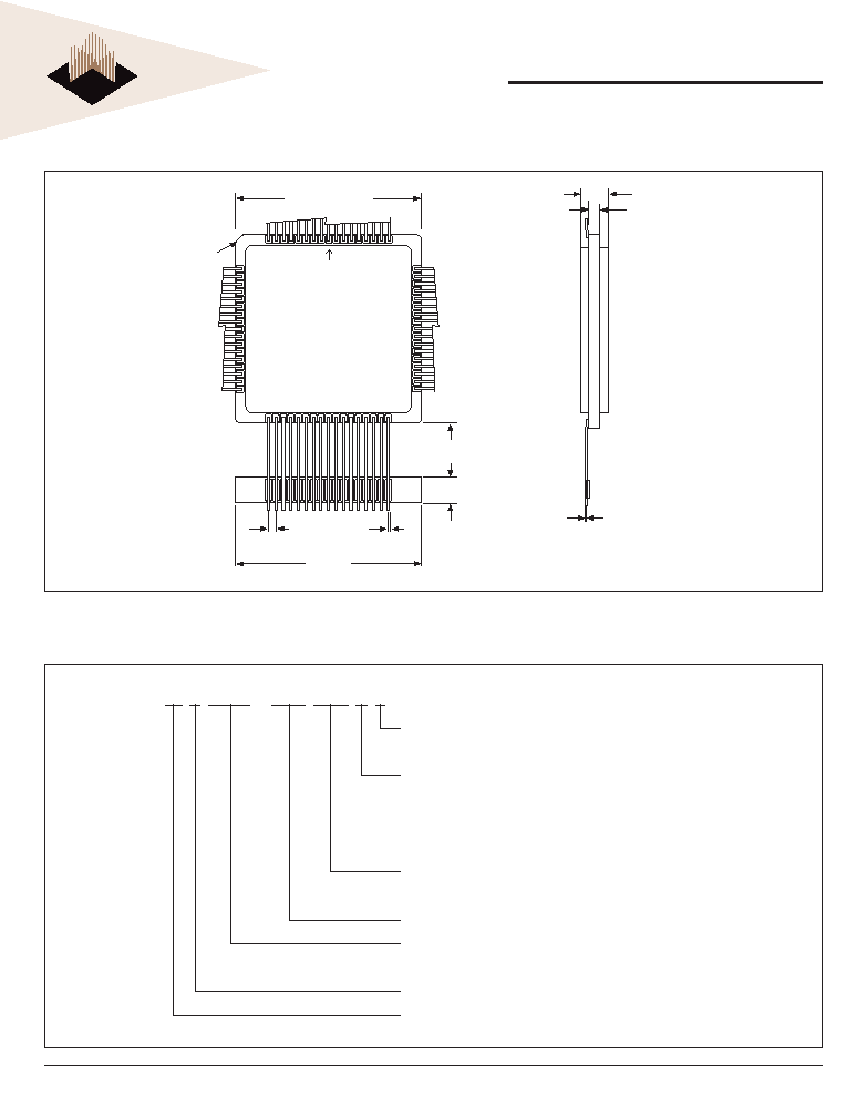
PACKAGE 503: 68 LEAD, CERAMIC QUAD FLAT PACK DUAL CAVITY, CQFP (G4D)
ALL LINEAR DIMENSIONS ARE MILLIMETERS AND PARENTHETICALLY IN INCHES
ORDERING INFORMATION
VPP PROGRAMMING VOLTAGE
5
=
5
V
DEVICE GRADE:
M = Military Screened -55įC to +125įC
I = Industrial
-40įC to +85įC
C
=
Commercial
0įC
to
+70įC
PACKAGE TYPE:
G4D = 40mm CQFP (Package 503)
ACCESS TIME (ns)
ORGANIZATION, 8M x 32
User confi gurable as 16M x 16 or 32M x 8
Flash
WHITE ELECTRONIC DESIGNS CORP.
W F 8M32 - XXX G4D X 5
5.2 (0.205) MAX
1.27 (0.050) Ī 0.1 (0.005)
0.010
+ 0.002
- 0.001
0.38 (0.015)
Ī 0.08 (0.003)
68 PLACES
1.27 (0.050)
TYP
39.6 (1.56) Ī 0.38 (0.015) SQ
38 (1.50) TYP
4 PLACES
5.1 (0.200)
Ī 0.25 (0.010)
4 PLACES
12.7 (0.500)
Ī 0.5 (0.020)
4 PLACES
PIN 1 IDENTIFIER
Pin 1