1
White Electronic Designs Corporation (602) 437-1520 www.whiteedc.com
White Electronic Designs
WME128K8-XXX
A
0-16
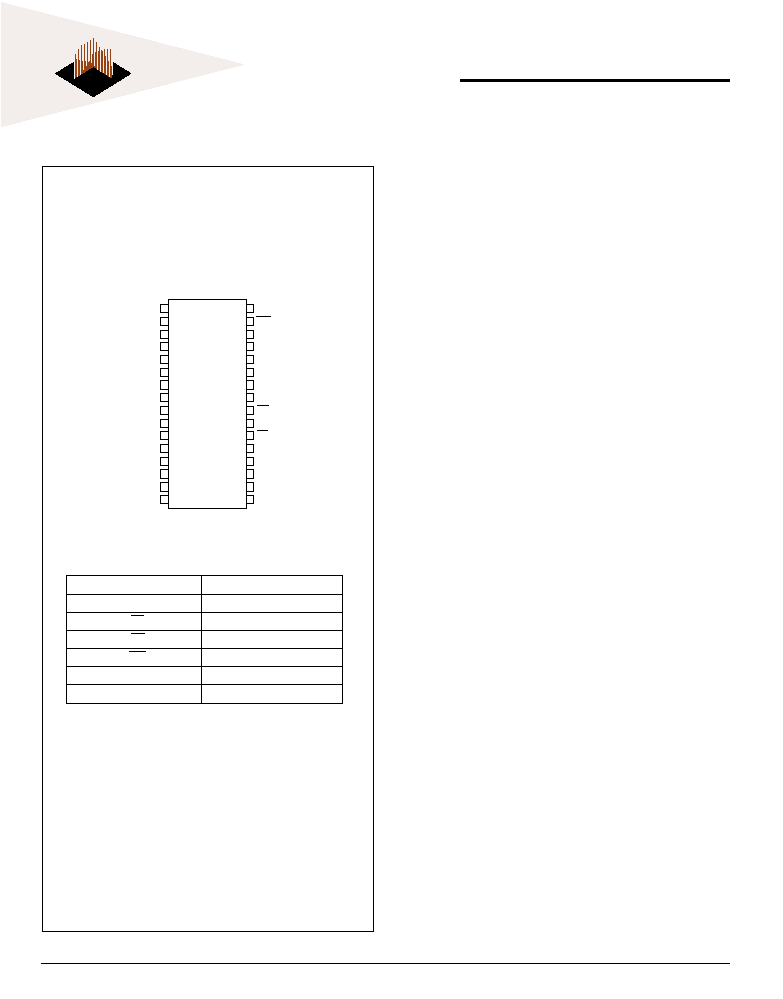
Address Inputs
I/O
0-7
Data Input/Output
CS
Chip Select
OE
Output Enable
WE
Write Enable
Vcc
+5.0V Power
V
SS
Ground
February 2002 Rev. 3
FEATURES
Read Access Times of 120, 140, 150, 200, 250, 300ns
JEDEC Approved Packages
32 pin, Hermetic Ceramic, 0.600" DIP (Package 300)
32 lead, Hermetic Ceramic, 0.400" SOJ (Package
101)
Commercial, Industrial and Military Temperature
Ranges
MIL-STD-883 Compliant Devices Available
Write Endurance 10,000 Cycles
Data Retention at 25�C, 10 Years
Low Power CMOS Operation
Automatic Page Write Operation
Internal Address and Data Latches for 128 Bytes
Internal Control Timer
Page Write Cycle Time 10ms Max.
Data Polling for End of Write Detection
Hardware and Software Data Protection
TTL Compatible Inputs and Outputs
FIG. 1
P
IN
C
ONFIGURATION
32 DIP
32 CSOJ
T
OP
V
IEW
1
2
3
4
5
6
7
8
9
10
11
12
13
14
15
16
32
31
30
29
28
27
26
25
24
23
22
21
20
19
18
17
NC
A16
A15
A12
A7
A6
A5
A4
A3
A2
A1
A0
I/O0
I/O1
I/O2
V
SS
V
CC
WE
NC
A14
A13
A8
A9
A11
OE
A10
CS
I/O7
I/O6
I/O5
I/O4
I/O3
P
IN
D
ESCRIPTION
128Kx8 CMOS MONOLITHIC EEPROM, SMD 5962-96796
2
White Electronic Designs Corporation Phoenix AZ (602) 437-1520
White Electronic Designs
WME128K8-XXX
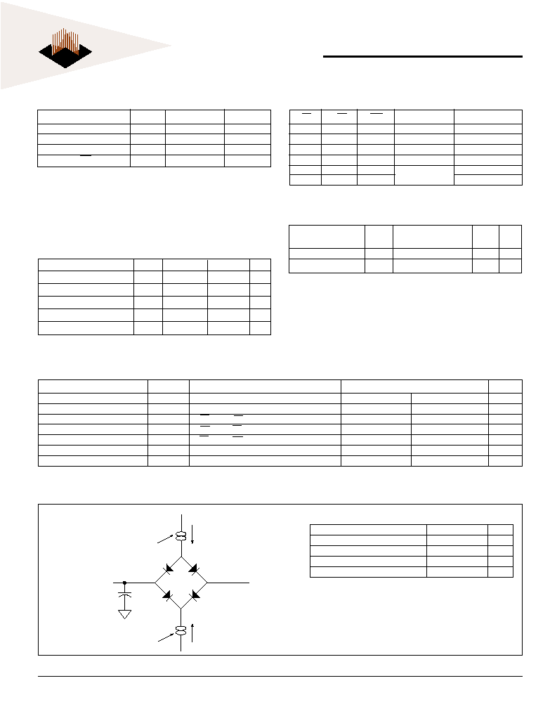
I
Current Source
D.U.T.
C = 50 pf
eff
I
OL
V
1.5V
(Bipolar Supply)
Z
Current Source
OH
FIG. 2
AC T
EST
C
IRCUIT
Parameter
Symbol
Conditions
Unit
Min
Max
Input Leakage Current
I
LI
V
CC
= 5.5, V
IN
= GND to V
CC
10
�A
Output Leakage Current
I
LO
CS = V
IH
, OE = V
IH
, V
OUT
= GND to V
CC
10
�A
Dynamic Supply Current
I
CC
CS = V
IL
, OE = V
IH
, f = 5MHz, Vcc = 5.5
80
mA
Standby Current
I
SB
CS = V
IH
, OE = V
IH
, f = 5MHz, Vcc = 5.5
0.625
mA
Output Low Voltage
V
OL
I
OL
= 2.1mA, Vcc = 4.5V
.45
V
Output High Voltage
V
OH
I
OH
= -400�A, Vcc = 4.5V
2.4
V
NOTE: DC test conditions: V
IH
= V
CC
-0.3V, V
IL
= 0.3V
T
RUTH
T
ABLE
A
BSOLUTE
M
AXIMUM
R
ATINGS
C
APACITANCE
(T
A
= +25�C)
NOTE:
Stresses above those listed under "Absolute Maximum Ratings" may
cause permanent damage to the device. This is a stress rating only
and functional operation of the device at these or any other conditions
above those indicated in the operational sections of this specification
is not implied. Exposure to absolute maximum rating conditions for
extended periods may affect device reliability.
DC C
HARACTERISTICS
(V
CC
= 5.0V, V
SS
= 0V, T
A
= -55�C
TO
+125�C)
RECOMMENDED OPERATING CONDITIONS
AC T
EST
C
ONDITIONS
Notes:
V
Z
is programmable from -2V to +7V.
I
OL
& I
OH
programmable from 0 to 16mA.
Tester Impedance Z
0
= 75 W.
V
Z
is typically the midpoint of V
OH
and V
OL
.
I
OL
& I
OH
are adjusted to simulate a typical resistive load circuit.
ATE tester includes jig capacitance.
Parameter
Symbol
Unit
Operating Temperature
T
A
-55 to +125
�C
Storage Temperature
T
STG
-65 to +150
�C
Signal Voltage Any Pin
V
G
-0.6 to + 6.25
V
Voltage on OE and A9
-0.6 to +13.5
V
CS
OE
WE
Mode
Data I/O
H
X
X
Standby
High Z
L
L
H
Read
Data Out
L
H
L
Write
Data In
X
H
X
Out Disable
High Z/Data Out
X
X
H
Write
X
L
X
Inhibit
Parameter
Sym
Condition
Unit
Max
Input Capacitance
C
IN
V
IN
= 0V, f = 1MHz
20
pF
Output Capacitance
C
OUT
V
I
/O
= 0V, f = 1MHz
20
pF
This parameter is guaranteed by design but not tested.
Parameter
Symbol
Min
Max
Unit
Supply Voltage
V
CC
4.5
5.5
V
Input High Voltage
V
IH
2.0
V
CC
+ 0.3
V
Input Low Voltage
V
IL
-0.3
+0.8
V
Operating Temp. (Mil.)
T
A
-55
+125
�C
Operating Temp. (Ind.)
T
A
-40
+85
�C
Parameter
Typ
Unit
Input Pulse Levels
V
IL
= 0, V
IH
= 3.0
V
Input Rise and Fall
5
ns
Input and Output Reference Level
1.5
V
Output Timing Reference Level
1.5
V
3
White Electronic Designs Corporation (602) 437-1520 www.whiteedc.com
White Electronic Designs
WME128K8-XXX
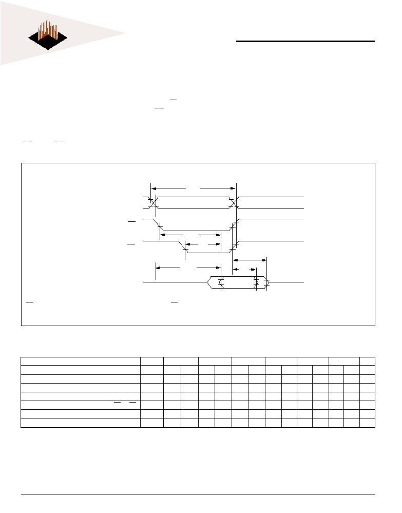
Parameter
Symbol -120 -140
-150 -200 -250 -300
Unit
Min
Max Min
Max
Min Max
Min Max Min Max Min Max
Read Cycle Time
t
RC
120
140
150
200
250
300
ns
Address Access Time
t
ACC
120
140
150
200
250
300
ns
Chip Select Access Time
t
ACS
120
140
150
200
250
300
ns
Output Hold from Address Change, OE or CS
t
OH
0
0
0
0
0
0
ns
Output Enable to Output Valid
t
OE
50
55
55
55
85
85
ns
Chip Select or Output Enable to High Z Output
t
DF
70
70
70
70
70
70
ns
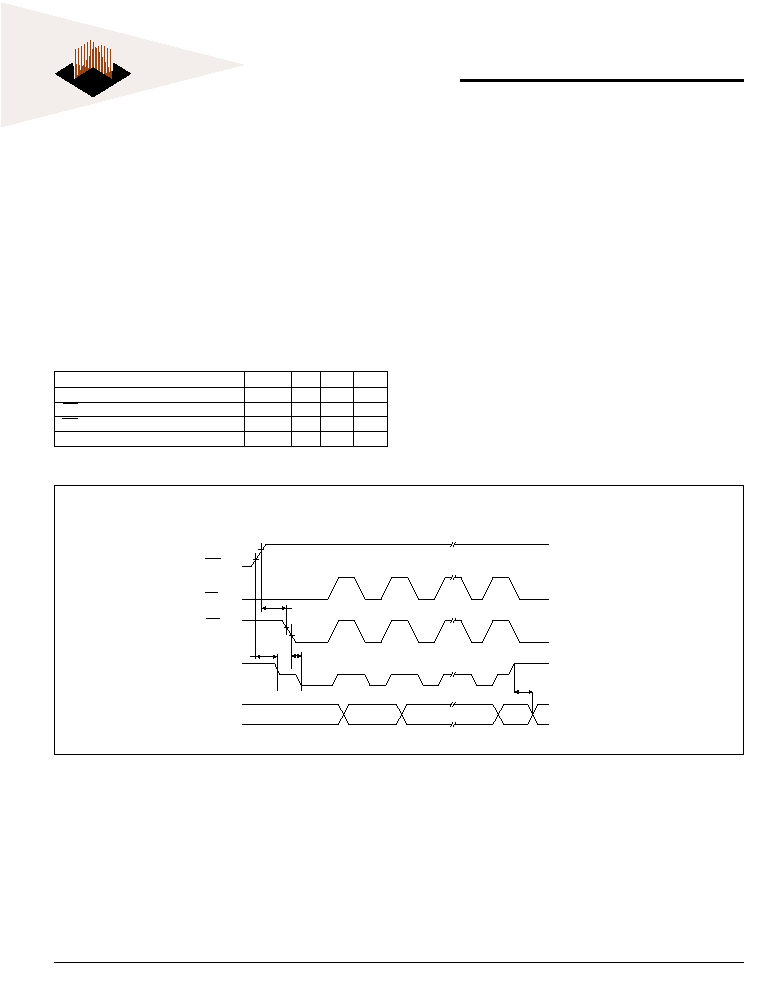
Figure 3 shows Read cycle waveforms. A read cycle be-
gins with selection address, chip select and output en-
able. Chip select is accomplished by placing the CS line
low. Output enable is done by placing the OE line low.
The memory places the selected data byte on I/O
0
through
I/O
7
after the access time. The output of the memory is
placed in a high impedance state shortly after either the
OE line or CS line is returned to a high level.
READ
AC R
EAD
C
HARACTERISTICS
(S
EE
F
IGURE
3)
(V
CC
= 5.0V, V
SS
= 0V, T
A
= -55�C
TO
+125�C)
FIG. 3 READ WAVEFORMS
t
ADDRESS
CS
OE
OUTPUT
OH
t
DF
t
ACC
t
RC
t
OE
t
ACS
OUTPUT
VALID
ADDRESS VALID
HIGH Z
NOTE:
OE may be delayed up to t
ACS
- t
OE
after the falling edge of CS
without impact on t
OE
or by t
ACC
- t
OE
after an address change without
impact on t
ACC
.
4
White Electronic Designs Corporation Phoenix AZ (602) 437-1520
White Electronic Designs
WME128K8-XXX
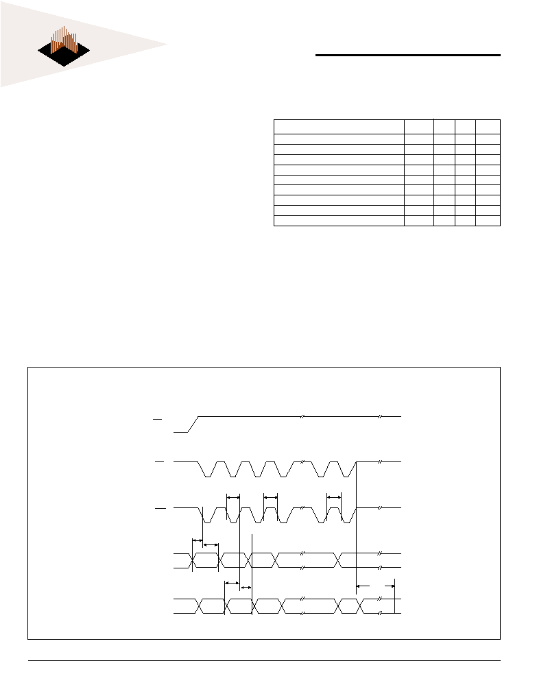
WRITE CYCLE TIMING
Figures 4 and 5 show the write cycle timing relation-
ships. A write cycle begins with address application,
write enable and chip select. Chip select is accom-
plished by placing the CS line low. Write enable con-
sists of setting the WE line low. The write cycle begins
when the last of either CS or WE goes low.
The WE line transition from high to low also initiates an
internal 150�sec delay timer to permit page mode op-
eration. Each subsequent WE transition from high to
low that occurs before the completion of the 150�sec
time out will restart the timer from zero. The operation
of the timer is the same as a retriggerable one-shot.
Write operations are initiated when both CS and WE
are low and OE is high. The EEPROM devices support
both a CS and WE controlled write cycle. The address
is latched by the falling edge of either CS or WE, which-
ever occurs last.
The data is latched internally by the rising edge of ei-
ther CS or WE, whichever occurs first. A byte write
operation will automatically continue to completion.
WRITE
AC WRITE CHARACTERISTICS
(V
CC
= 5.0V, V
SS
= 0V, T
A
= -55�C
TO
+125�C)
Parameter
Symbol 128Kx8
Unit
Min
Max
Write Cycle Time, TYP = 6ms
t
WC
10
ms
Address Set-up Time
t
AS
10
ns
Write Pulse Width (WE or CS)
t
WP
150
ns
Chip Select Set-up Time
t
CS
0
ns
Address Hold Time
t
AH
100
ns
Data Hold Time
t
DH
10
ns
Chip Select Hold Time
t
CH
0
ns
Data Set-up Time
t
DS
100
ns
Output Enable Set-up Time
t
OES
10
ns
Output Enable Hold Time
t
OEH
10
ns
Write Pulse Width High
t
WPH
50
ns

5
White Electronic Designs Corporation (602) 437-1520 www.whiteedc.com
White Electronic Designs
WME128K8-XXX
FIG. 4 WRITE WAVEFORMS WE CONTROLLED
t
ADDRESS (1)
CS
WE
DATA IN
DH
t
WPH
t
WP
t
CSH
t
OEH
t
AH
t
OES
t
AS
t
CS
OE
t
WC
t
DS
t
ADDRESS
WE
CS
DATA IN
DH
t
WPH
t
WP
t
CSH
t
OEH
t
AH
t
OES
t
AS
t
CS
OE
t
DS
t
WC
FIG. 5 WRITE WAVEFORMS CS CONTROLLED
NOTE:
1. Decoded Address Lines must be valid for the duration of the write.
6
White Electronic Designs Corporation Phoenix AZ (602) 437-1520
White Electronic Designs
WME128K8-XXX
DATA POLLING
The WME128K8-XXX offers a data polling feature which
allows a faster method of writing to the device. Figure
6 shows the timing diagram for this function. During a
byte or page write cycle, an attempted read of the last
byte written will result in the complement of the written
data on I/O7. Once the write cycle has been completed,
true data is valid on all outputs and the next cycle may
begin. Data polling may begin at any time during the
write cycle.
DATA POLLING CHARACTERISTICS
(V
CC
= 5.0V, V
CC
= 0V, T
A
= -55�C
TO
+125�C)
FIG. 6 DATA POLLING WAVEFORMS
Parameter
Symbol Min
Max Unit
Data Hold Time
t
DH
10
ns
OE Hold Time
t
OEH
10
ns
OE To Output Valid
t
OE
55
ns
Write Recovery Time
t
WR
0
ns
WE
t
OEH
t
DH
t
OE
t
WR
HIGH Z
CS
OE
I/O
7
ADDRESS
7
White Electronic Designs Corporation (602) 437-1520 www.whiteedc.com
White Electronic Designs
WME128K8-XXX
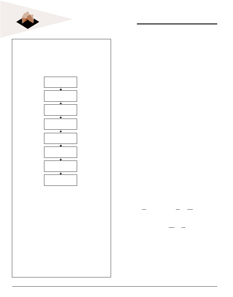
PAGE WRITE OPERATION
The WME128K8-XXX has a page write operation that
allows one to 128 bytes of data to be written into the
device and consecutively loads during the internal pro-
gramming period. Successive bytes may be loaded in
the same manner after the first data byte has been
loaded. An internal timer begins a time out operation at
each write cycle. If another write cycle is completed
within 150�s or less, a new time out period begins. Each
write cycle restarts the delay period. The write cycles
can be continued as long as the interval is less than the
time out period.
The usual procedure is to increment the least signifi-
cant address lines from A0 through A6 at each write
cycle. In this manner a page of up to 128 bytes can be
loaded in to the EEPROM in a burst mode before be-
ginning the relatively long interval programming cycle.
After the 150�s time out is completed, the EEPROM
begins an internal write cycle. During this cycle the
entire page of bytes will be written at the same time.
The internal programming cycle is the same regardless
of the number of bytes accessed.
PAGE WRITE CHARACTERISTICS
(V
CC
= 5.0V, V
SS
= 0V, T
A
= -55�C
TO
+125�C)
FIG. 7 PAGE MODE WRITE WAVEFORMS
1. Page address must remain valid for duration of write cycle.
Page Mode Write Characteristics
Symbol
Unit
Parameter
Min Max
Write Cycle Time, TYP = 6ms
t
WC
10
ms
Address Set-up Time
t
AS
10
ns
Address Hold Time (1)
t
AH
100
ns
Data Set-up Time
t
DS
100
ns
Data Hold Time
t
DH
10
ns
Write Pulse Width
t
WP
150
ns
Byte Load Cycle Time
t
BLC
150
�s
Write Pulse Width High
t
WPH
50
ns
OE
BYTE 0
BYTE 1
BYTE 2
BYTE 3
VALID DATA
VALID
ADDRESS
t
WC
t
BLC
t
WPH
t
WP
ADDRESS
DATA
CS
WE
BYTE 127
t
DS
t
DH
t
AS
t
AH

8
White Electronic Designs Corporation Phoenix AZ (602) 437-1520
White Electronic Designs
WME128K8-XXX
FIG. 8 SOFTWARE DATA
PROTECTION ENABLE ALGORITHM
(1)
NOTES:
1. Data Format: I/O
7
-I/O
0
(Hex);
Address Format: A
16
-A
0
(Hex).
2. Write Protect state will be activated at end of write even if no
other data is loaded.
3. Write Protect state will be deactivated at end of write period
even if no other data is loaded.
4. 1 to 128 bytes of data may be loaded.
LOAD DATA AA
TO
ADDRESS 5555
LOAD DATA 55
TO
ADDRESS 2AAA
LOAD DATA A0
TO
ADDRESS 5555
LOAD DATA XX
TO
ANY ADDRESS
(4)
LOAD LAST BYTE
TO
LAST ADDRESS
WRITES ENABLED
(2)
ENTER DATA
PROTECT STATE
9
White Electronic Designs Corporation (602) 437-1520 www.whiteedc.com
White Electronic Designs
WME128K8-XXX
HARDWARE DATA PROTECTION
These features protect against inadvertent writes to the
WME128K8-XXX. These are included to improve reli-
ability during normal operation:
a) VCC power on delay
As VCC climbs past 3.8V typical the device will wait
5msec typical before allowing write cycles.
b) VCC sense
While below 3.8V typical write cycles are inhibited.
c) Write inhibiting
Holding OE low and either CS or WE high inhibits
write cycles.
d) Noise filter
Pulses of <15ns (typ) on WE or CS will not initiate a
write cycle.
FIG. 9 SOFTWARE BLOCK
DATA PROTECTION DISABLE
ALGORITHM
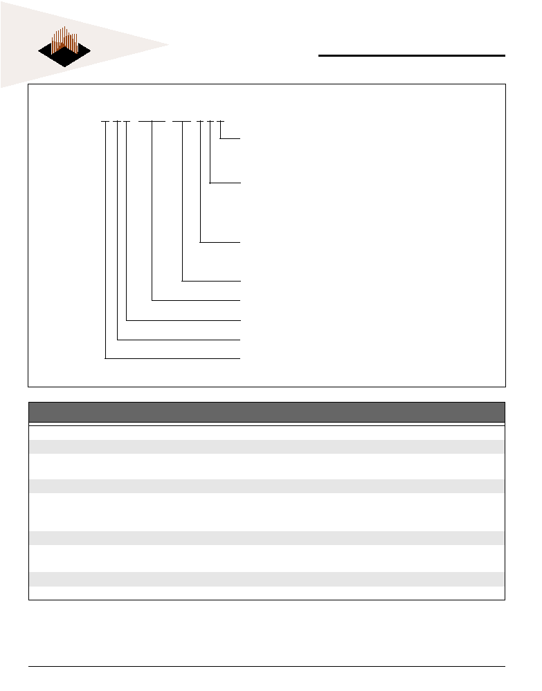
SOFTWARE DATA PROTECTION
A software write protection feature may be enabled or
disabled by the user. When shipped by White Micro-
electronics, the WME128K8-XXX has the feature dis-
abled. Write access to the device is unrestricted.
To enable software write protection, the user writes three
access code bytes to three special internal locations.
Once write protection has been enabled, each write to
the EEPROM must use the same three byte write se-
quence to permit writing. After setting software Data
protection, any attempt to write to the device without
the three-byte command sequence will start the inter-
nal write timers. No Data will be written to the device;
however, for the duration of tWC. The write protection
feature can be disabled by a six byte write sequence of
specific data to specific locations. Power transitions
will not reset the software write protection.
The software write protection guards against inadvert-
ent writes during power transitions or unauthorized
modification using a PROM programmer.
NOTES:
1. Data Format: I/O
7
-I/O
0
(Hex);
Address Format: A
16
-A
0
(Hex).
2. Write Protect state will be activated at end of write even if no
other data is loaded.
3. Write Protect state will be deactivated at end of write period
even if no other data is loaded.
4. 1 to 128 bytes of data may be loaded.
LOAD DATA AA
TO
ADDRESS 5555
LOAD DATA 55
TO
ADDRESS 2AAA
LOAD DATA 80
TO
ADDRESS 5555
LOAD DATA AA
TO
ADDRESS 5555
LOAD DATA 55
TO
ADDRESS 2AAA
LOAD DATA 20
TO
ADDRESS 5555
LOAD DATA XX
TO
ANY ADDRESS
(4)
LOAD LAST BYTE
TO
LAST ADDRESS
(3)
EXIT DATA
PROTECT STATE

10
White Electronic Designs Corporation Phoenix AZ (602) 437-1520
White Electronic Designs
WME128K8-XXX
ALL LINEAR DIMENSIONS ARE MILLIMETERS AND PARENTHETICALLY IN INCHES
PACKAGE 101: 32 LEAD, CERAMIC SOJ
1.27 (0.050) TYP
21.1 (0.830) � 0.25 (0.010)
PIN 1 IDENTIFIER
19.1 (0.750) TYP
11.3 (0.446)
� 0.2 (0.009)
3.96 (0.156) MAX
0.2 (0.008)
� 0.05 (0.002)
9.55 (0.376) � 0.25 (0.010)
1.27 (0.050) � 0.25 (0.010)
0.89 (0.035)
Radius TYP
PACKAGE 300: 32 PIN, CERAMIC DIP, SINGLE CAVITY SIDE BRAZED
42.4 (1.670) � 0.4 (0.016)
PIN 1 IDENTIFIER
0.84 (0.033)
� 0.4 (0.014)
4.34 (0.171) � 0.79 (0.031)
15.04 (0.592)
� 0.3 (0.012)
ALL LINEAR DIMENSIONS ARE MILLIMETERS AND PARENTHETICALLY IN INCHES
11
White Electronic Designs Corporation (602) 437-1520 www.whiteedc.com
White Electronic Designs
WME128K8-XXX
LEAD FINISH:
Blank = Gold plated leads
A = Solder dip leads
DEVICE GRADE:
Q = MIL-STD-883 Compliant
M = Military Screened
-55�C to +125�C
I = Industrial
-40�C to +85�C
C = Commercial
0�C to +70�C
PACKAGE TYPE:
C = 32 Pin Ceramic DIP (Package 300)
DE = 32 Lead CSOJ (Package 101)
ACCESS TIME (ns)
ORGANIZATION 128K x 8
EEPROM
MONOLITHIC
WHITE ELECTRONIC DESIGNS CORP.
O
RDERING
I
NFORMATION
DEVICE TYPE
SPEED
PACKAGE
SMD NO.
128K x 8 EEPROM Monolithic
300ns
32 pin DIP (C)
5962-96796 01HYX
128K x 8 EEPROM Monolithic
250ns
32 pin DIP (C)
5962-96796 02HYX
128K x 8 EEPROM Monolithic
200ns
32 pin DIP (C)
5962-96796 03HYX
128K x 8 EEPROM Monolithic
150ns
32 pin DIP (C)
5962-96796 04HYX
128K x 8 EEPROM Monolithic
140ns
32 pin DIP (C)
5962-96796 05HYX
128K x 8 EEPROM Monolithic
120ns
32 pin DIP (C)
5962-96796 06HYX
128K x 8 EEPROM Monolithic
300ns
32 lead SOJ (DE)
5962-96796 01HXX
128K x 8 EEPROM Monolithic
250ns
32 lead SOJ (DE)
5962-96796 02HXX
128K x 8 EEPROM Monolithic
200ns
32 lead SOJ (DE)
5962-96796 03HXX
128K x 8 EEPROM Monolithic
150ns
32 lead SOJ (DE)
5962-96796 04HXX
128K x 8 EEPROM Monolithic
140ns
32 lead SOJ (DE)
5962-96796 05HXX
128K x 8 EEPROM Monolithic
120ns
32 lead SOJ (DE)
5962-96796 06HXX
W M E 128K8 - XXX X X X