1
White Electronic Designs Corporation ∑ (602) 437-1520 ∑ www.whiteedc.com
HI-RELIABILITY PRODUCT
WMF128K8-XXX5
128Kx8 MONOLITHIC FLASH, SMD 5962-96690
FEATURES
s Access Times of 50*, 60, 70, 90, 120, 150ns
s Packaging
∑ 32 lead, Hermetic Ceramic, 0.400" SOJ (Package 101)
∑ 32 pin, Hermetic Ceramic, 0.600" DIP (Package 300)
∑ 32 lead, Flatpack (Package 220)
∑ 32 lead, Formed Flatpack (Package 221)
∑ 32 pin, Rectangular Ceramic Leadless Chip Carrier
(Package 601)
s 100,000 Erase/Program Cycles Minimum
s Sector Erase Architecture
∑ 8 equal size sectors of 16KBytes each
∑ Any combination of sectors can be concurrently
erased. Also supports full chip erase
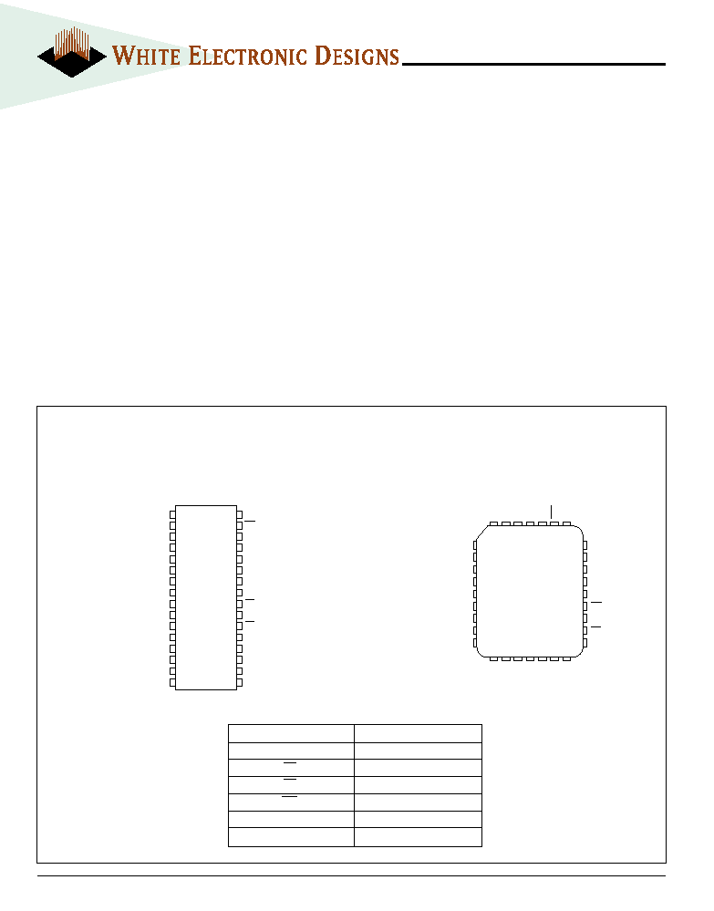
PIN CONFIGURATION FOR WMF128K8-XXX5
A
0
-
16
Address Inputs
I/O
0-7
Data Input/Output
CS
Chip Select
OE
Output Enable
WE
Write Enable
V
CC
+5.0V Power
V
SS
Ground
PIN DESCRIPTION
TOP VIEW
32 DIP
32 CSOJ
32 FLATPACK
1
2
3
4
5
6
7
8
9
10
11
12
13
14
15
16
32
31
30
29
28
27
26
25
24
23
22
21
20
19
18
17
NC
A16
A15
A12
A7
A6
A5
A4
A3
A2
A1
A0
I/O0
I/O1
I/O2
V
SS
V
CC
WE
NC
A14
A13
A8
A9
A11
OE
A10
CS
I/O7
I/O6
I/O5
I/O4
I/O3
5
6
7
8
9
10
11
12
13
29
28
27
26
25
24
23
22
21
4
3
2
1 32 31 30
14 15 16 17 18 19 20
A7
A6
A5
A4
A3
A2
A1
A0
I/O
0
I/O1
I/O2
V
SS
I/O3
I/O4
I/O5
I/O6
A14
A13
A8
A9
A11
OE
A10
CS
I/O7
A12
A15
A16
NC
V
CC
WE
NC
PIN CONFIGURATION FOR WMF128K8-XCLX5
TOP VIEW
32 CLCC
s Organized as 128Kx8
s Commercial, Industrial and Military Temperature Ranges
s 5 Volt Programming. 5V
±
10% Supply.
s Low Power CMOS
s Embedded Erase and Program Algorithms
s TTL Compatible Inputs and CMOS Outputs
s Page Program Operation and Internal Program Control Time.
Note: For programming information refer to Flash Programming 1M5
Application Note.
* The access time of 50ns is available in Industrial and Commercial
temperature ranges only.
April 2001 Rev. 5
2
White Electronic Designs Corporation ∑ (602) 437-1520 ∑ www.whiteedc.com
WMF128K8-XXX5
ABSOLUTE MAXIMUM RATINGS (1)
NOTES:
1. Stresses above the absolute maximum rating may cause permanent damage
to the device. Extended operation at the maximum levels may degrade
performance and affect reliability.
2. Minimum DC voltage on input or I/O pins is -0.5V. During voltage transitions,
inputs may overshoot V
SS
to -2.0 V for periods of up to 20ns. Maximum DC
voltage on output and I/O pins is V
CC
+ 0.5V. During voltage transitions,
outputs may overshoot to Vcc + 2.0 V for periods of up to 20ns.
3. Minimum DC input voltage on A
9
pin is -0.5V. During voltage transitions, A
9
may
overshoot Vss to -2V for periods of up to 20ns. Maximum DC input voltage on A
9
is +13.5V which may overshoot to 14.0 V for periods up to 20ns.
DC CHARACTERISTICS - CMOS COMPATIBLE
(V
CC
= 5.0V, V
SS
= 0V, T
A
= -55
∞
C to +125
∞
C)
Parameter
Unit
Operating Temperature
-55 to +125
∞
C
Supply Voltage Range (V
CC
)
-2.0 to +7.0
V
Signal voltage range (any pin except A9) (2)
-2.0 to +7.0
V
Storage Temperature Range
-65 to +150
∞
C
Lead Temperature (soldering, 10 seconds)
+300
∞
C
Data Retention Mil Temp
10
years
Endurance (write/erase cycles) Mil Temp
10,000 min.
cycles
A
9
Voltage for sector protect (V
ID
) (3)
-2.0 to +14.0
V
Parameter
Symbol
Conditions
Min
Max
Unit
Input Leakage Current
I
LI
V
CC
= 5.5, V
IN
= GND to V
CC
10
µ
A
Output Leakage Current
I
LO
V
CC
= 5.5, V
IN
= GND to V
CC
10
µ
A
V
CC
Active Current for Read
(1)
I
CC1
CS = V
IL
, OE = V
IH
35
mA
V
CC
Active Current for Program
I
CC2
CS = V
IL
, OE = V
IH
50
mA
or Erase
(2)
V
CC
Standby Current
I
CC3
V
CC
= 5.5, CS = V
IH
, f = 5MHz
1.6
mA
Output Low Voltage
V
OL
I
OL
= 8.0 mA, V
CC
= 4.5
0.45
V
Output High Voltage
V
OH1
I
OH
= -2.5 mA, V
CC
= 4.5
0.85 x V
CC
V
Output High Voltage
V
OH2
I
OH
= -100
µ
A, V
CC
= 4.5
V
CC
- 0.4
V
Low V
CC
Lock Out Voltage
V
LKO
3.2
V
CAPACITANCE
(T
A
= +25
∞
C)
Parameter
Symbol
Conditions
Max
Unit
Address Input capacitance
C
AD
V
I/O
= 0 V, f = 1.0 MHz
15
pF
Output Enable capacitance
C
OE
V
IN
= 0 V, f = 1.0 MHz
15
pF
Write Enable capacitance
C
WE
V
IN
= 0 V, f = 1.0 MHz
15
pF
Chip Select capacitance
C
CS
V
IN
= 0 V, f = 1.0 MHz
15
pF
Data I/O capacitance
C
I/O
V
I/O
= 0 V, f = 1.0 MHz
15
pF
This parameter is guaranteed by design but not tested.
RECOMMENDED OPERATING CONDITIONS
Parameter
Symbol
Min
Max
Unit
Supply Voltage
V
CC
4.5
5.5
V
Input High Voltage
V
IH
2.0
V
CC
+ 0.3
V
Input Low Voltage
V
IL
-0.5
+0.8
V
Operating Temp. (Mil.)
T
A
-55
+125
∞
C
Operating Temp. (Ind.)
T
A
-40
+85
∞
C
A
9
Voltage for Sector Protect
V
ID
11.5
12.5
V
NOTES:
1. The I
CC
current listed includes both the DC operating current and the frequency dependent component (at 5 MHz).
The frequency component typically is less than 2 mA/MHz, with OE at V
IH
.
2. I
CC
active while Embedded Algorithm (program or erase) is in progress.
3. DC test conditions: V
IL
= 0.3V, V
IH
= V
CC
- 0.3V
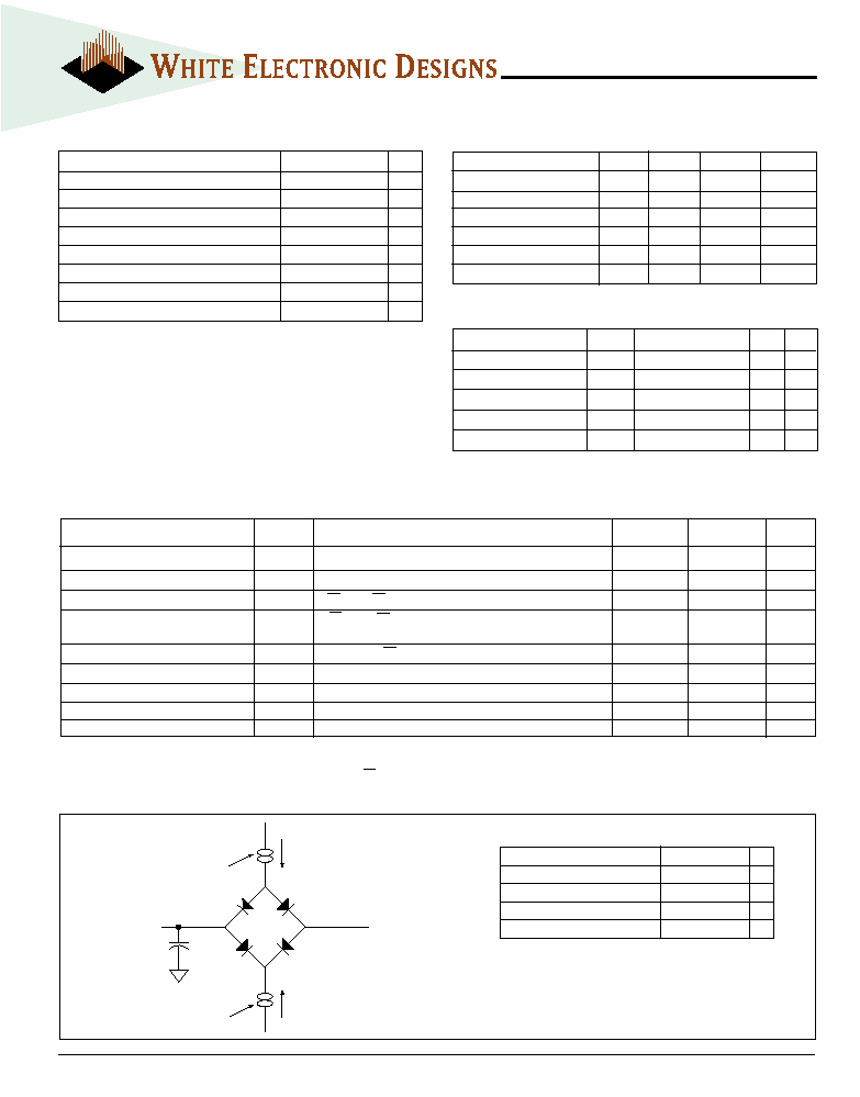
AC TEST CIRCUIT
AC TEST CONDITIONS
I
Current Source
D.U.T.
C = 50 pf
eff
I
OL
V
1.5V
(Bipolar Supply)
Z
Current Source
OH
NOTES:
V
Z
is programmable from -2V to +7V.
I
OL
& I
OH
programmable from 0 to 16mA.
Tester Impedance Z
0
= 75
.
V
Z
is typically the midpoint of V
OH
and V
OL
.
I
OL
& I
OH
are adjusted to simulate a typical resistive load circuit.
ATE tester includes jig capacitance.
Parameter
Typ
Unit
Input Pulse Levels
V
IL
= 0, V
IH
= 3.0
V
Input Rise and Fall
5
ns
Input and Output Reference Level
1.5
V
Output Timing Reference Level
1.5
V

3
White Electronic Designs Corporation ∑ (602) 437-1520 ∑ www.whiteedc.com
WMF128K8-XXX5
AC CHARACTERISTICS ≠ WRITE/ERASE/PROGRAM OPERATIONS, WE CONTROLLED
(V
CC
= 5.0V, V
SS
= 0V, T
A
= -55
∞
C to +125
∞
C)
Parameter
Symbol
-50
-60
-70
-90
-120
-150
Unit
Min
Max
Min
Max
Min
Max
Min
Max
Min
Max
Min
Max
Write Cycle Time
t
AVAV
t
WC
50
60
70
90
120
150
ns
Chip Select Setup Time
t
ELWL
t
CS
0
0
0
0
0
0
ns
Write Enable Pulse Width
t
WLWH
t
WP
25
30
35
45
50
50
ns
Address Setup Time
t
AVWL
t
AS
0
0
0
0
0
0
ns
Data Setup Time
t
DVWH
t
DS
25
30
30
45
50
50
ns
Data Hold Time
t
WHDX
t
DH
0
0
0
0
0
0
ns
Address Hold Time
t
WLAX
t
AH
40
45
45
45
50
50
ns
Chip Select Hold Time
t
WHEH
t
CH
0
0
0
0
0
0
ns
Write Enable Pulse Width High
t
WHWL
t
WPH
20
20
20
20
20
20
ns
Duration of Byte Programming Operation (min) t
WHWH1
14
14
14
14
14
14
µ
s
Sector Erase Time
t
WHWH2
2.2
60
2.2
60
2.2
60
2.2
60
2.2
60
2.2
60
sec
Read Recovery Time Before Write
t
GHWL
0
0
0
0
0
0
ns
V
CC
Setup Time
t
VCS
50
50
50
50
50
50
µ
s
Chip Programming Time
12.5
12.5
12.5
12.5
12.5
12.5
sec
Output Enable Setup Time
t
OES
0
0
0
0
0
0
ns
Output Enable Hold Time (1)
t
OEH
10
10
10
10
10
10
ns
1. For Toggle and Data Polling.
Parameter
Symbol
-50
-60
-70
-90
-120
-150
Unit
Min
Max
Min
Max
Min
Max
Min
Max
Min
Max
Min
Max
Read Cycle Time
t
AVAV
t
RC
50
60
70
90
120
150
ns
Address Access Time
t
AVQV
t
ACC
50
60
70
90
120
150
ns
Chip Select Access Time
t
ELQV
t
CE
50
60
70
90
120
150
ns
OE to Output Valid
t
GLQV
t
OE
25
30
35
40
50
55
ns
Chip Select to Output High Z (1)
t
EHQZ
t
DF
20
20
20
25
30
35
ns
OE High to Output High Z (1)
t
GHQZ
t
DF
20
20
20
25
30
35
ns
Output Hold from Address, CS or OE Change,
t
AXQX
t
OH
0
0
0
0
0
0
ns
whichever is first
1. Guaranteed by design, not tested.
AC CHARACTERISTICS ≠ READ ONLY OPERATIONS
(V
CC
= 5.0V, V
SS
= 0V, T
A
= -55
∞
C to +125
∞
C)
4
White Electronic Designs Corporation ∑ (602) 437-1520 ∑ www.whiteedc.com
AC CHARACTERISTICS ≠ WRITE/ERASE/PROGRAM OPERATIONS, CS CONTROLLED
(V
CC
= 5.0V, V
SS
= 0V, T
A
= -55
∞
C to +125
∞
C)
Parameter
Symbol
-50
-60
-70
-90
-120
-150
Unit
Min
Max
Min
Max
Min
Max
Min
Max
Min
Max
Min
Max
Write Cycle Time
t
AVAV
t
WC
50
60
70
90
120
150
ns
WE Setup Time
t
WLEL
t
WS
0
0
0
0
0
0
ns
CS Pulse Width
t
ELEH
t
CP
25
30
35
45
50
50
ns
Address Setup Time
t
AVEL
t
AS
0
0
0
0
0
0
ns
Data Setup Time
t
DVEH
t
DS
25
30
30
45
50
50
ns
Data Hold Time
t
EHDX
t
DH
0
0
0
0
0
0
ns
Address Hold Time
t
ELAX
t
AH
40
45
45
45
50
50
ns
WE Hold from WE High
t
EHWH
t
WH
0
0
0
0
0
0
ns
CS Pulse Width High
t
EHEL
t
CPH
20
20
20
20
20
20
ns
Duration of Programming Operation
t
WHWH1
14
14
14
14
14
14
µ
s
Duration of Erase Operation
t
WHWH2
2.2
60
2.2
60
2.2
60
2.2
60
2.2
60
2.2
60
sec
Read Recovery before Write
t
GHEL
0
0
0
0
0
0
ns
Chip Programming Time
12.5
12.5
12.5
12.5
12.5
12.5
sec
WMF128K8-XXX5
5
White Electronic Designs Corporation ∑ (602) 437-1520 ∑ www.whiteedc.com
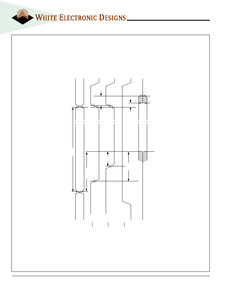
AC WAVEFORMS FOR READ OPERATIONS
Addresses
CS
OE
WE
Outputs
High Z
Addresses Stable
t
OE
t
RC
Output Valid
t
CE
t
ACC
t
OH
High Z
t
DF
WMF128K8-XXX5