1
White Electronic Designs Corporation (602) 437-1520 www.whiteedc.com
WMF512K8-XXX5
White Electronic Designs
512Kx8 MONOLITHIC FLASH, SMD 5962-96692
FEATURES
Access Times of 60, 70, 90, 120, 150ns
Packaging
32 pin, Hermetic Ceramic, 0.600" DIP
(Package 300)
32 lead, Hermetic Ceramic, 0.400" SOJ
(Package 101)
32 pin, Rectangular Ceramic Leadless Chip
Carrier (Package 601)
32 lead Flatpack (Package 220)
1,000,000 Erase/Program Cycles Minimum
Sector Erase Architecture
8 equal size sectors of 64K bytes each
Any combination of sectors can be concurrently
erased. Also supports full chip erase
Organized as 512Kx8
Commercial, Industrial and Military Temperature
Ranges
5 Volt Programming. 5V ± 10% Supply.
Low Power CMOS
Embedded Erase and Program Algorithms
TTL Compatible Inputs and CMOS Outputs
Page Program Operation and Internal Program
Control Time.
Note: For programming information refer to Flash Programming 4M5
Application Note.
January 2003 Rev. 4
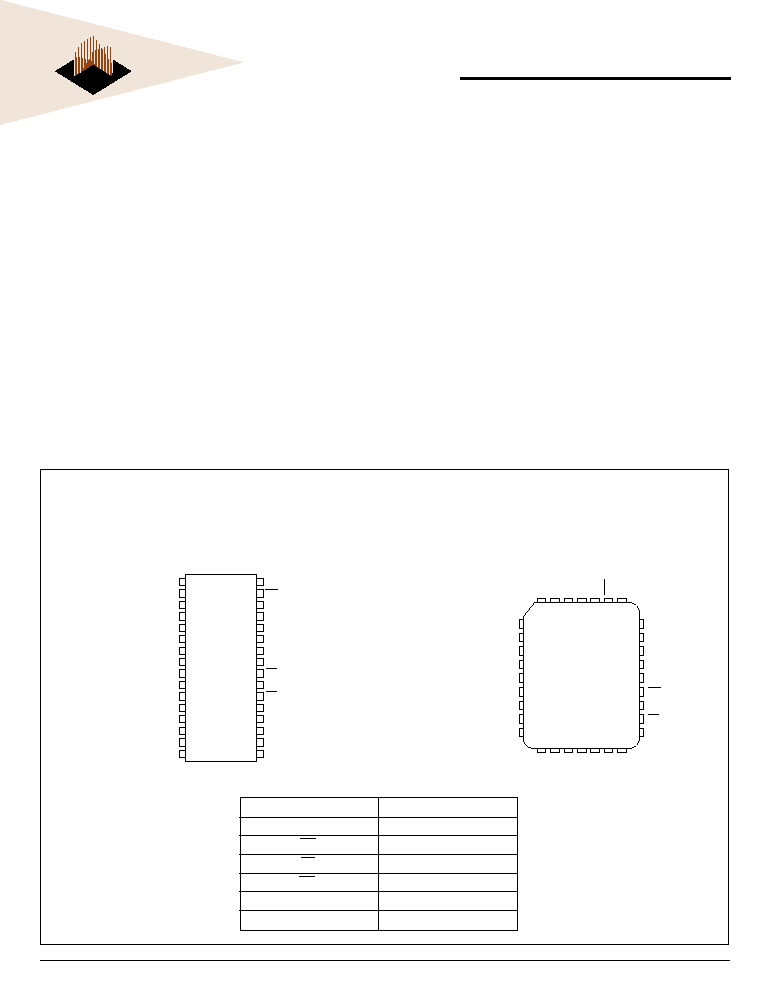
PIN CONFIGURATION FOR WMF512K8-XXX5
A
0
-
18
Address Inputs
I/O
0-7
Data Input/Output
CS
Chip Select
OE
Output Enable
WE
Write Enable
V
CC
+5.0V Power
V
SS
Ground
P
IN
D
ESCRIPTION
1
2
3
4
5
6
7
8
9
10
11
12
13
14
15
16
32
31
30
29
28
27
26
25
24
23
22
21
20
19
18
17
A18
A16
A15
A12
A7
A6
A5
A4
A3
A2
A1
A0
I/O0
I/O1
I/O2
V
SS
V
CC
WE
A17
A14
A13
A8
A9
A11
OE
A10
CS
I/O7
I/O6
I/O5
I/O4
I/O3
T
OP
V
IEW
32 DIP
32 CSOJ
32 Flatpack
5
6
7
8
9
10
11
12
13
29
28
27
26
25
24
23
22
21
4 3 2 1 32 31 30
14 15 16 17 18 19 20
A7
A6
A5
A4
A3
A2
A1
A0
I/O
0
I/O1
I/O2
V
SS
I/O3
I/O4
I/O5
I/O6
A14
A13
A8
A9
A11
OE
A10
CS
I/O7
A12
A15
A16
A18
V
CC
WE
A17
PIN CONFIGURATION FOR WMF512K8-XCLX5
T
OP
V
IEW
32 CLCC

2
White Electronic Designs Corporation Phoenix AZ (602) 437-1520
WMF512K8-XXX5
White Electronic Designs
A
BSOLUTE
M
AXIMUM
R
ATINGS
(1)
DC C
HARACTERISTICS
- CMOS C
OMPATIBLE
(V
CC
= 5.0V, V
SS
= 0V, T
A
= -55∞C
TO
+125∞C)
Parameter
Unit
Operating Temperature
-55 to +125
∞C
Supply Voltage (V
CC
) (1)
-2.0 to +7.0
V
Signal Voltage Range(any pin except A
9
) (2)
-2.0 to +7.0
V
Storage Temperature Range
-65 to +150
∞C
Lead Temperature (soldering, 10 seconds)
+300
∞C
Data Retention Mil Temp
20
years
Endurance - erase/program cycles (Mil Temp)
100,000 min
cycles
A
9
Voltage for sector protect (V
ID
) (3)
-2.0 to +14.0
V
Parameter
Symbol
Conditions
Unit
Min
Max
Input Leakage Current
I
LI
V
CC
= 5.5, V
IN
= GND to V
CC
10
µA
Output Leakage Current
I
LOx32
V
CC
= 5.5, V
IN
= GND to V
CC
10
µA
V
CC
Active Current for Read (1)
I
CC1
CS = V
IL
, OE = V
IH
, f = 5MHz
50
mA
V
CC
Active Current for Program
I
CC2
CS = V
IL
, OE = V
IH
60
mA
or Erase
(2)
V
CC
Standby Current
I
CC4
V
CC
= 5.5, CS = V
IH
, f = 5MHz
1.6
mA
Output Low Voltage
V
OL
I
OL
= 8.0 mA, V
CC
= 4.5
0.45
V
Output High Voltage
V
OH1
I
OH
= -2.5 mA, V
CC
= 4.5
0.85 x V
CC
V
Low V
CC
Lock-Out Voltage
V
LKO
3.2
4.2
V
R
ECOMMENDED
O
PERATING
C
ONDITIONS
Parameter
Symbol
Min
MaxUnit
Supply Voltage
V
CC
4.5
5.5
V
Input High Voltage
V
IH
2.0
Vcc + 0.5
V
Input Low Voltage
V
IL
-0.5
+0.8
V
Operating Temp. (Mil.)
T
A
-55
+125
∞C
Operating Temp. (Ind.)
T
A
-40
+85
∞C
A
9
Voltage for Sector Protect
V
ID
11.5
12.5
V
NOTES:
1. Stresses above the absolute maximum rating may cause permanent
damage to the device. Extended operation at the maximum levels may
degrade performance and affect reliability.
2. Minimum DC voltage on input or I/O pins is -0.5V. During voltage
transitions, inputs may overshoot V
SS
to -2.0 V for periods of up to
20ns. Maximum DC voltage on output and I/O pins is V
CC
+ 0.5V.
During voltage transitions, outputs may overshoot to Vcc + 2.0 V for
periods of up to 20ns.
3. Minimum DC input voltage on A9 pin is -0.5V. During voltage
transitions, A9 may overshoot Vss to -2V for periods of up to 20ns.
C
APACITANCE
(T
A
= +25∞C)
Parameter
Symbol
Conditions
MaxUnit
Address Input capacitance
C
AD
V
I/O
= 0 V, f = 1.0 MHz 15
pF
Output Enable capacitance C
OE
V
IN
= 0 V, f = 1.0 MHz 15
pF
Write Enable capacitance C
WE
V
IN
= 0 V, f = 1.0 MHz 15
pF
Chip Select capacitance
C
CS
V
IN
= 0 V, f = 1.0 MHz 15
pF
Data I/O capacitance
C
I/O
V
I/O
= 0 V, f = 1.0 MHz 15
pF
This parameter is guaranteed by design but not tested.
NOTES:
1. The I
CC
current listed includes both the DC operating current and the frequency dependent component (at 5 MHz). The frequency
component typically is less than 2 mA/MHz, with OE at V
IH
.
2. I
CC
active while Embedded Algorithm (program or erase) is in progress.
3. DC test conditions: V
IL
= 0.3V, V
IH
= V
CC
- 0.3V
3
White Electronic Designs Corporation (602) 437-1520 www.whiteedc.com
WMF512K8-XXX5
White Electronic Designs
Parameter
Symbol
-60
-70
-90
-120
-150
Unit
Min
Max Min
MaxMin
MaxMin
MaxMin Max
Write Cycle Time
t
AVAV
t
WC
60
70
90
120
150
ns
Write Enable Setup Time
t
WLEL
t
WS
0
0
0
0
0
ns
Chip Select Pulse Width
t
ELEH
t
CP
40
45
45
50
50
ns
Address Setup Time
t
AVEL
t
AS
0
0
0
0
0
ns
Data Setup Time
t
DVEH
t
DS
40
45
45
50
50
ns
Data Hold Time
t
EHDX
t
DH
0
0
0
0
0
ns
Address Hold Time
t
ELAX
t
AH
40
45
45
50
50
ns
Chip Select Pulse Width High
t
EHEL
t
CPH
20
20
20
20
20
ns
Duration of Byte Programming Operation (1)
t
WHWH1
300
300
300
300
300
µs
Sector Erase Time (2)
t
WHWH2
15
15
15
15
15
sec
Read Recovery Time
t
GHEL
0
0
0
0
0
ns
Chip Programming Time
11
11
11
11
11
sec
Chip Erase Time (3)
64
64
64
64
64
sec
NOTES:
1. Typical value for t
WHWH1
is 7µs.
2. Typical value for t
WHWH2
is 1sec.
3. Typical value for Chip Erase time is 8sec.
AC C
HARACTERISTICS
W
RITE
/E
RASE
/P
ROGRAM
O
PERATIONS
,CS C
ONTROLLED
(V
CC
= 5.0V, V
SS
= 0V, T
A
= -55∞C
TO
+125∞C)
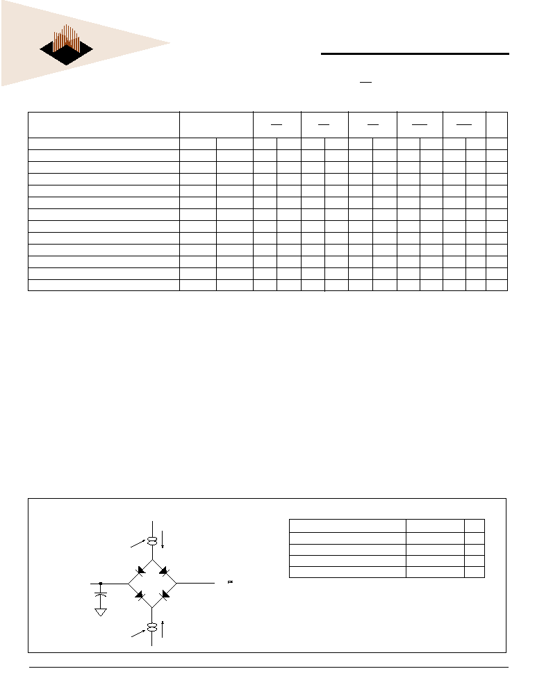
AC TEST CIRCUIT
AC T
EST
C
ONDITIONS
Notes:
V
Z
is programmable from -2V to +7V.
I
OL
& I
OH
programmable from 0 to 16mA.
Tester Impedance Z
0
= 75 W.
V
Z
is typically the midpoint of V
OH
and V
OL
.
I
OL
& I
OH
are adjusted to simulate a typical resistive load circuit.
ATE tester includes jig capacitance.
Parameter
Typ
Unit
Input Pulse Levels
V
IL
= 0, V
IH
= 3.0
V
Input Rise and Fall
5
ns
Input and Output Reference Level
1.5
V
Output Timing Reference Level
1.5
V
I
Current Source
D.U.T.
C = 50 pf
eff
I
OL
V 1.5V
(Bipolar Supply)
Z
Current Source
OH
4
White Electronic Designs Corporation Phoenix AZ (602) 437-1520
WMF512K8-XXX5
White Electronic Designs
Parameter
Symbol
-60
-70
-90
-120
-150
Unit
Min
MaxMin
MaxMin
MaxMin
MaxMin Max
Read Cycle Time
t
AVAV
t
RC
60
70
90
120
150
ns
Address Access Time
t
AVQV
t
ACC
60
70
90
120
150
ns
Chip Select Access Time
t
ELQV
t
CE
60
70
90
120
150
ns
Output Enable to Output Valid
t
GLQV
t
OE
35
35
35
50
55
ns
Chip Select to Output High Z (1)
t
EHQZ
t
DF
20
20
20
30
35
ns
Output Enable High to Output High Z (1)
t
GHQZ
t
DF
20
20
20
30
35
ns
Output Hold from Address, CS or OE
t
AXQX
t
OH
0
0
0
0
0
ns
Change, whichever is First
NOTES:
1. Guaranteed by design, but not tested
Parameter
Symbol
-60
-70
-90
-120
-150
Unit
Min
MaxMin
MaxMin
MaxMin
MaxMin Max
Write Cycle Time
t
AVAV
t
WC
60
70
90
120
150
ns
Chip Select Setup Time
t
ELWL
t
CS
0
0
0
0
0
ns
Write Enable Pulse Width
t
WLWH
t
WP
40
45
45
50
50
ns
Address Setup Time
t
AVWH
t
AS
0
0
0
0
0
ns
Data Setup Time
t
DVWH
t
DS
40
45
45
50
50
ns
Data Hold Time
t
WHDX
t
DH
0
0
0
0
0
ns
Address Hold Time
t
WHAX
t
AH
40
45
45
50
50
ns
Write Enable Pulse Width High
t
WHWL
t
WPH
20
20
20
20
20
ns
Duration of Byte Programming Operation (1)
t
WHWH1
300
300
300
300
300
µs
Sector Erase Time (2)
t
WHWH2
15
15
15
15
15
sec
Read Recovery Time before Write
t
GHWL
0
0
0
0
0
ms
V
CC
Set-up Time
tvcs
50
50
50
50
50
µs
Chip Programming Time
11
11
11
11
11
sec
Output Enable Setup Time
t
OES
0
0
0
0
0
ns
Output Enable Hold Time (4)
t
OEH
10
10
10
10
10
ns
Chip Erase Time (3)
64
64
64
64
64
sec
NOTES:
1. Typical value for t
WHWH1
is 7µs.
2. Typical value for t
WHWH2
is 1sec.
3. Typical value for Chip Erase time is 8sec.
4. For Toggle and Data Polling.
AC C
HARACTERISTICS
W
RITE
/E
RASE
/P
ROGRAM
O
PERATIONS
, WE C
ONTROLLED
(V
CC
= 5.0V, T
A
= -55∞C
TO
+125∞C)
AC C
HARACTERISTICS
R
EAD
O
NLY
O
PERATIONS
(V
CC
= 5.0V, T
A
= -55∞C
TO
+125∞C)
5
White Electronic Designs Corporation (602) 437-1520 www.whiteedc.com
WMF512K8-XXX5
White Electronic Designs
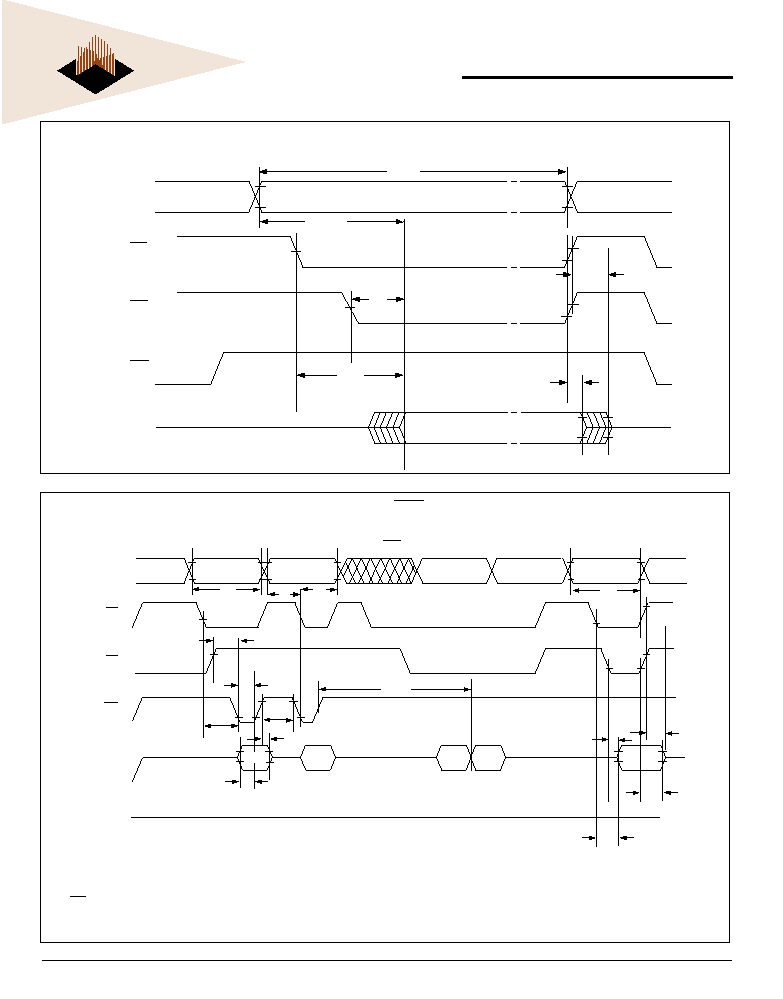
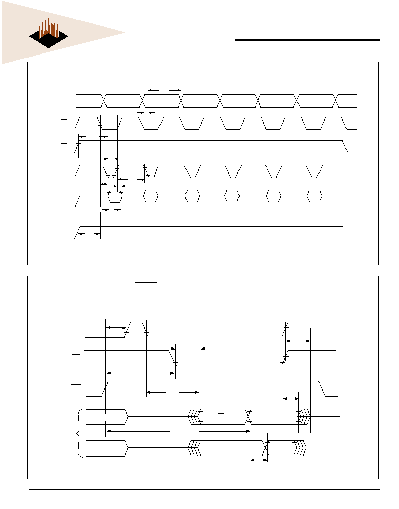
AC WAVEFORMS FOR READ OPERATIONS
Addresses
CS
OE
WE
Outputs
High Z
Addresses Stable
t
OE
t
RC
Output Valid
t
CE
t
ACC
t
OH
High Z
t
DF
NOTES:
1. PA is the address of the memory location to be programmed.
2. PD is the data to be programmed at byte address.
3. I/O
7
is the output of the complement of the data written to the device.
4. I/O
OUT
is the output of the data written to the device.
5. Figure indicates last two bus cycles of four bus cycle sequence.
WRITE/ERASE/PROGRAM OPERATION, WE CONTROLLED
Addresses
CS
OE
WE
Data
5.0 V
5555H
PA
PA
t
WC
t
CS
PD
I/O
7
I/O
OUT
t
AH
t
WPH
t
DH
t
DS
Data Polling
t
AS
t
RC
t
WP
A0H
t
OE
t
DF
t
OH
t
CE
t
GHWL
t
WHWH1
6
White Electronic Designs Corporation Phoenix AZ (602) 437-1520
WMF512K8-XXX5
White Electronic Designs
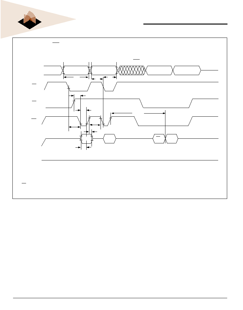
CS
OE
WE
t
OE
t
OE
t
CE
t
CH
t
OH
I/O
7
I/O
7
=
Valid Data
High Z
I/O
0-6
= Invalid
I/O
0-7
Valid Data
t
DF
I/O
7
I/O
0-6
t
OEH
t
WHWH 1 or 2
Data
AC WAVEFORMS FOR DATA POLLING DURING EMBEDDED
ALGORITHM OPERATIONS
AC WAVEFORMS CHIP/SECTOR ERASE OPERATIONS
Addresses
CS
OE
WE
Data
V
CC
5555H
2AAAH
2AAAH
SA
5555H
5555H
t
WP
t
CS
t
VCS
10H/30H
55H
80H
55H
AAH
AAH
t
AH
t
AS
t
GHWL
t
WPH
t
DH
t
DS
Notes:
1. SA is the Sector Address for Sector Erase.
7
White Electronic Designs Corporation (602) 437-1520 www.whiteedc.com
WMF512K8-XXX5
White Electronic Designs
Notes:
1. PA represents the address of the memory location to be programmed.
2. PD represents the data to be programmed at byte address.
3. I/O
7
is the output of the complement of the data written to the device.
4. I/O
OUT
is the output of the data written to the device.
5. Figure indicates the last two bus cycles of a four bus cycle sequence.
Addresses
WE
OE
CS
Data
5.0 V
5555H
PA
PA
t
WC
t
WS
PD
I/O
7
I/O
OUT
t
AH
t
CPH
t
CP
t
DH
t
DS
Data Polling
t
AS
t
GHEL
A0H
t
WHWH1
ALTERNATE CS CONTROLLED PROGRAMMING OPERATION TIMINGS
8
White Electronic Designs Corporation Phoenix AZ (602) 437-1520
WMF512K8-XXX5
White Electronic Designs
ALL LINEAR DIMENSIONS ARE MILLIMETERS AND PARENTHETICALLY IN INCHES
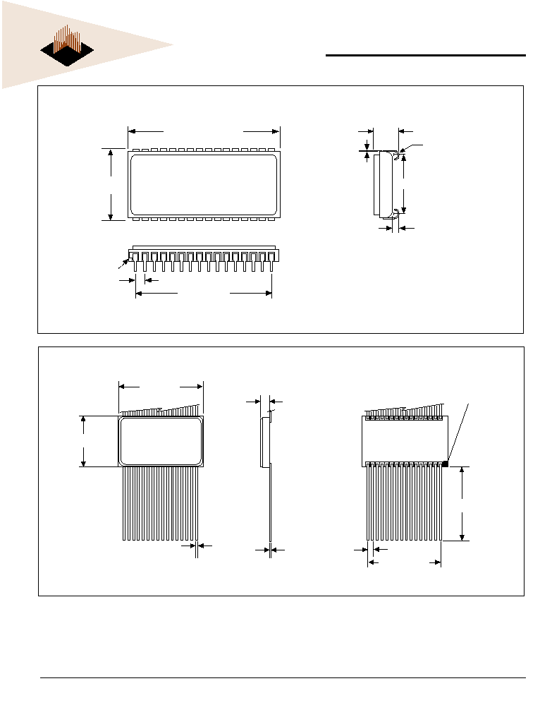
PACKAGE 101: 32 LEAD, CERAMIC SOJ
1.27 (0.050) TYP
21.1 (0.830)
±
0.25 (0.010)
19.1 (0.750) TYP
11.3 (0.442)
±
0.30 (0.012)
3.96 (0.156) MAX
0.2 (0.008)
±
0.05 (0.002)
9.55 (0.376)
±
0.25 (0.010)
1.27 (0.050)
±
0.25 (0.010)
0.89 (0.035)
Radius TYP
PIN 1 IDENTIFIER
PACKAGE 220: 32 LEAD, CERAMIC FLATPACK
ALL LINEAR DIMENSIONS ARE MILLIMETERS AND PARENTHETICALLY IN INCHES
10.41 (0.410)
± 0.13 (0.005)
2.60 (0.102) MAX
0.127 (0.005)
+ 0.05 (0.002)
≠
0.025 (0.001)
PIN 1
IDENTIFIER
1.27 (0.050) TYP
19.05 (0.750) TYP
10.16 (0.400)
± 0.51 (0.020)
0.43 (0.017)
± 0.05 (0.002)
20.83 (0.820)
± 0.25 (0.010)
9
White Electronic Designs Corporation (602) 437-1520 www.whiteedc.com
WMF512K8-XXX5
White Electronic Designs
PACKAGE 300: 32 PIN, CERAMIC DIP, SINGLE CAVITY SIDE BRAZED
2.5 (0.100)
TYP
1.27 (0.050)
±
0.1 (0.005)
0.46 (0.018)
±
0.05 (0.002)
0.84 (0.033)
±
0.4 (0.014)
3.2 (0.125) MIN
15.04 (0.592)
±
0.3 (0.012)
0.25 (0.010)
±
0.05 (0.002)
15.25 (0.600)
±
0.25 (0.010)
42.4 (1.670)
±
0.4 (0.016)
4.34 (0.171)
±
0.79 (0.031)
PIN 1 IDENTIFIER
ALL LINEAR DIMENSIONS ARE MILLIMETERS AND PARENTHETICALLY IN INCHES
10
White Electronic Designs Corporation Phoenix AZ (602) 437-1520
WMF512K8-XXX5
White Electronic Designs
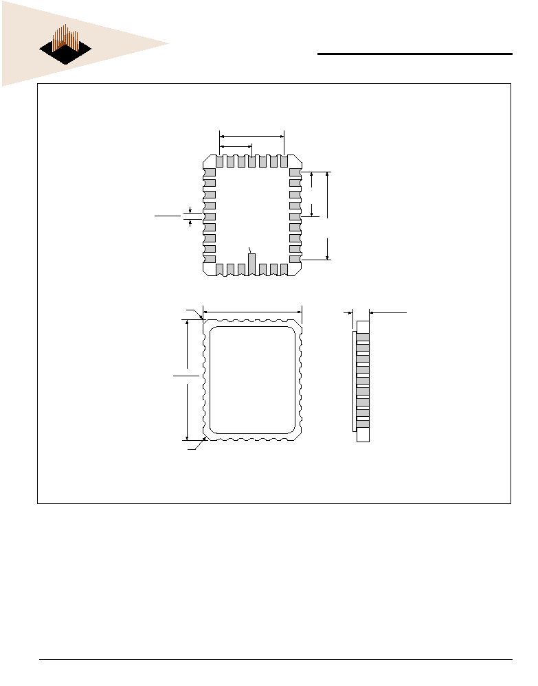
ALL LINEAR DIMENSIONS ARE MILLIMETERS AND PARENTHETICALLY IN INCHES
PACKAGE 601: 32 PIN, RECTANGULAR CERAMIC LEADLESS CHIP CARRIER
7.62 (0.300) TYP
5.08
(0.200)
TYP
3.81
(0.150) TYP
10.16
(0.400)
TYP
0.38 (0.015) x 45
∞
PIN 1 IDENTIFIER
0.56 (0.022)
0.71 (0.028)
11.25 (0.443)
14.15 (0.557)
13.79 (0.543)
14.15 (0.557)
1.63 (0.064)
2.54 (0.100)
PIN 1
1.02 (0.040) x 45
∞
3 PLACES

11
White Electronic Designs Corporation (602) 437-1520 www.whiteedc.com
WMF512K8-XXX5
White Electronic Designs
WHITE ELECTRONIC DESIGNS CORP.
MONOLITHIC
Flash
ORGANIZATION, 512K x 8
ACCESS TIME (ns)
PACKAGE TYPE:
C = 32 Pin Ceramic DIP (Package 300)
CL = 32 Pin Rectangular Ceramic Leadless Chip Carrier (Package 601)
DE = 32 Lead Ceramic SOJ (Package 101)
FE = 32 Lead Flatpack (Package 220)
DEVICE GRADE:
M = Military Screened
-55∞C to +125∞C
I = Industrial
-40∞C to +85∞C
C = Commercial
0∞C to +70∞C
V
PP
PROGRAMMING VOLTAGE
5 = 5V
LEAD FINISH:
Blank = Gold plated leads
A = Solder dip leads
ORDERING INFORMATION
W M F 512K 8 - XXX X X 5 X
DEVICE TYPE
SECTOR SIZE SPEED
PACKAGE
SMD NO.
512K x 8 Flash Monolithic
64KByte
150ns
32 pin DIP (C)
5962-96692 01HXX
512K x 8 Flash Monolithic
64KByte
120ns
32 pin DIP (C)
5962-96692 02HXX
512K x 8 Flash Monolithic
64KByte
90ns
32 pin DIP (C)
5962-96692 03HXX
512K x 8 Flash Monolithic
64KByte
70ns
32 pin DIP (C)
5962-96692 04HXX
512K x 8 Flash Monolithic
64KByte
150ns
32 lead SOJ (DE)
5962-96692 01HYX
512K x 8 Flash Monolithic
64KByte
120ns
32 lead SOJ (DE)
5962-96692 02HYX
512K x 8 Flash Monolithic
64KByte
90ns
32 lead SOJ (DE)
5962-96692 03HYX
512K x 8 Flash Monolithic
64KByte
70ns
32 lead SOJ (DE)
5962-96692 04HYX
512K x 8 Flash Monolithic
64KByte
150ns
32 lead Flatpack (FE)
5962-96692 01HUX
512K x 8 Flash Monolithic
64KByte
120ns
32 lead Flatpack (FE)
5962-96692 02HUX
512K x 8 Flash Monolithic
64KByte
90ns
32 lead Flatpack (FE)
5962-96692 03HUX
512K x 8 Flash Monolithic
64KByte
70ns
32 lead Flatpack (FE)
5962-96692 04HUX

12
White Electronic Designs Corporation Phoenix AZ (602) 437-1520
WMF512K8-XXX5
White Electronic Designs
Document Title
512K x 8 Flash Monolithic
Revision History
Rev #
History
Release Date
Status
Initial Release
September 1996
Preliminary
Changes (Pg. 1)
May 1997
Final
1.1
Change status to Final
Changes (Pg. 1)
February 1998
Final
1.1
Correct typo of Ceramic
Changes (Pg. 10)
April 1998
Final
1.1
Remove pedestal from Flatpack package drawing
Changes (Pg. 1)
February 1999
Final
1.1
Change name from FP to Flatpack
Rev 2
Changes (Pg. 1, 2, 3, 4, 13)
May 1999
Final
1.1
Change number of max program/erases to 1,000,000
1.2
Change temperature of max program/erases to 25C
1.3
Absolute Maximum Ratings Table:
1.3.1 Change Data Retention to 20years
1.3.2 Change Endurance to 100,000 cycles minimum
1.4
Write/Erase/Program Operations Tables:
1.4.1 Change t
WHWH
1
to 300ms
1.4.2 Add Note (1) Typical t
WHWH
1
= 7ms
1.4.3 Change t
WHWH2
to 15sec
1.4.4 Add Note (2) Typical t
WHWH2
= 1 sec
1.4.5 Change Chip Programming Time to 11 sec
1.4.6 Change Chip Erase Time too 64 sec
1.4.7 Add Note (3) Chip Erase Time = 8 sec
1.5
Ordering Information
1.5.1 Change Company Name to White EDC
1.6
Change Title Style to new WEDC look
Rev 3
Changes (Pg. 1, 2, 10, 12, 13)
May 1999
Final
1.1
Change package 206 to package 220
1.2
Remove temperature range notice for Endurance
1.3
Change width spec to 0.457" minimum for package 601
Rev 4
Changes (Pg. 1, 3, 4)
January 2003
Final
1.1
Add 60ns speed grade option