1
White Electronic Designs Corporation ∑ (602) 437-1520 ∑ www.wedc.com
White Electronic Designs
WS128K32-XXX
June 2004
Rev. 4
128Kx32 SRAM MODULE, SMD 5962-93187
5
Volt
Power
Supply
Low
Power
CMOS
TTL Compatible Inputs and Outputs
Built in Decoupling Caps and Multiple Ground Pins
for Low Noise Operation
Weight
WS128K32-XG2UX - 8 grams typical
WS128K32-XH1X - 13 grams typical
WS128K32-XG4TX - 20 grams typical
Upgradeable to 512Kx32
FEATURES
Access Times of 70, 85, 100, 120ns
MIL-STD-883 Compliant Devices Available
Packaging
∑ 66-pin, PGA Type, 1.075 inch square, Hermetic
Ceramic HIP (Package 400).
∑ 68 lead, 40mm Low Profi le CQFP, 3.56mm
(0.140")(Package 502).
∑ 68 lead, Hermetic CQFP (G2U), 22.4mm
(0.880 inch) square, 4.57mm (0.140 inch) high,
(Package 510)
Organized as 128Kx32; User Confi gurable as
256Kx16 or 512Kx8
Commercial,
Industrial
and
Military
Temperature
Ranges
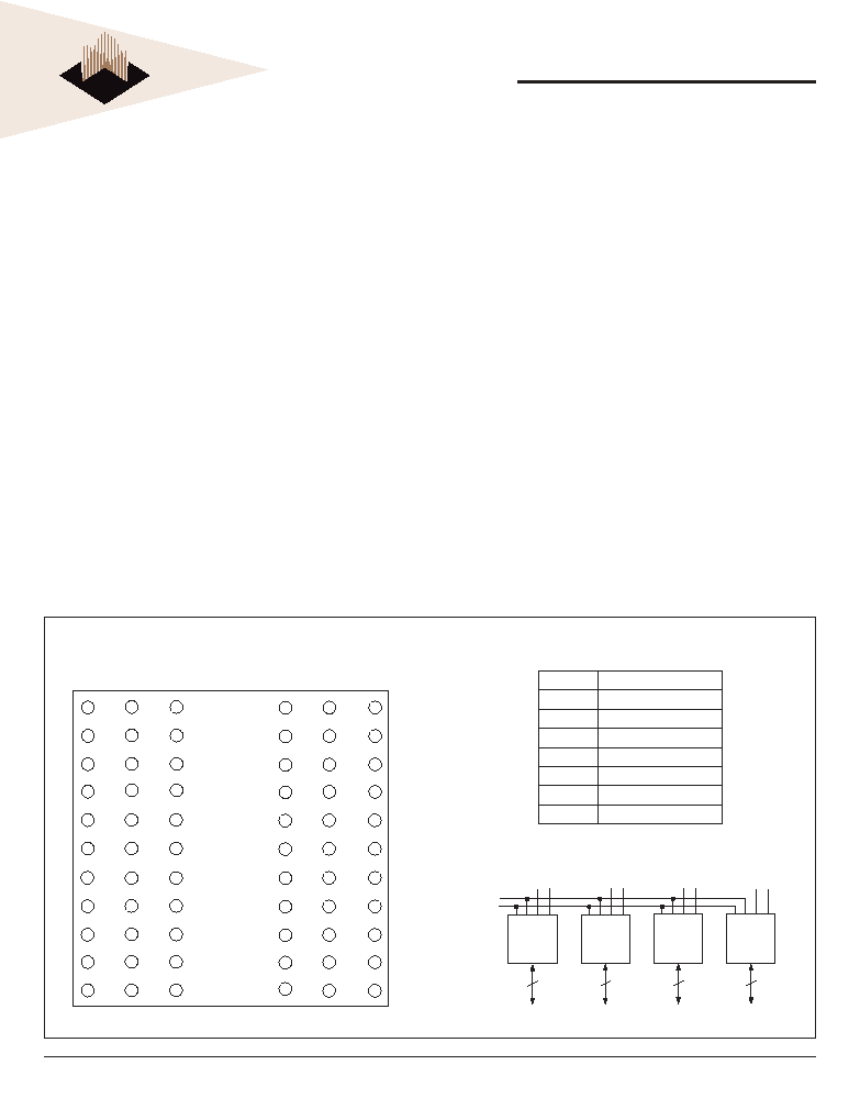
Pin Description
Block Diagram
Top View
FIGURE 1 ≠ PIN CONFIGURATION FOR WS128K32N-XH1X
I/O
8
I/O
9
I/O
10
A
14
A
16
A
11
A
0
NC
I/O
0
I/O
1
I/O
2
WE
2
#
CS
2
#
GND
I/O
11
A
10
A
9
A
15
V
CC
CS
1
#
NC
I/O
3
I/O
15
I/O
14
I/O
13
I/O
12
OE#
NC
WE
1
#
I/O
7
I/O
6
I/O
5
I/O
4
I/O
24
I/O
25
I/O
26
A
7
A
12
NC
A
13
A
8
I/O
16
I/O
17
I/O
18
V
CC
CS
4
#
WE
4
#
I/O
27
A
4
A
5
A
6
WE
3
#
CS
3
#
GND
I/O
19
I/O
31
I/O
30
I/O
29
I/O
28
A
1
A
2
A
3
I/O
23
I/O
22
I/O
21
I/O
20
11 22 33 44 55 66
1 12 23 34 45 56
WE
1
# CS
1
#
CS
2
#
CS
3
#
CS
4
#
WE
4
#
WE
3
#
WE
2
#
128K x 8
128K x 8
128K x 8
128K x 8
OE#
A
0-16
I/O
0-7
I/O
24-31
I/O
16-23
I/O
8-15
8
8
8
8
I/O
0-31
Data Inputs/Outputs
A
0-16
Address Inputs
WE
1-4
#
Write Enables
CS
1-4
#
Chip Selects
OE#
Output Enable
V
CC
Power Supply
GND Ground
NC
Not Connected

2
White Electronic Designs Corporation ∑ (602) 437-1520 ∑ www.wedc.com
White Electronic Designs
WS128K32-XXX
June 2004
Rev. 4
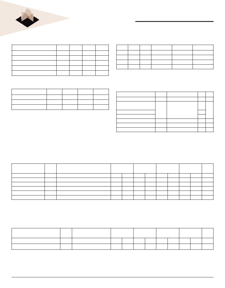
FIGURE 2 ≠ PIN CONFIGURATION FOR WS128K32-XG4TX
FIGURE 3 ≠ PIN CONFIGURATION FOR WS128K32-XG2UX
TOP VIEW
PIN DESCRIPTION
BLOCK DIAGRAM
Top View
Pin Description
Block Diagram
128K X 8
8
8
8
8
128K X 8
128K X 8
128K X 8
WE#
OE#
A
0-16
CS
1
#
CS
2
#
CS
3
#
CS
4
#
I/O
0 - 7
I/O
8 - 15
I/O
16 - 23
I/O
24 - 31
WE
1
# CS
1
#
CS
2
#
CS
3
#
CS
4
#
WE
4
#
WE
3
#
WE
2
#
128K x 8
128K x 8
128K x 8
128K x 8
OE#
A
0-16
I/O
0-7
I/O
24-31
I/O
16-23
I/O
8-15
8
8
8
8
I/O
0
I/O
1
I/O
2
I/O
3
I/O
4
I/O
5
I/O
6
I/O
7
GND
I/O
8
I/O
9
I/O
10
I/O
11
I/O
12
I/O
13
I/O
14
I/O
15
I/O
16
I/O
17
I/O
18
I/O
19
I/O
20
I/O
21
I/O
22
I/O
23
GND
I/O
24
I/O
25
I/O
26
I/O
27
I/O
28
I/O
29
I/O
30
I/O
31
V
CC
A
11
A
12
A
13
A
14
A
15
A
16
CS
1
#
OE#
CS
2
#
NC
WE
2
#
WE
3
#
WE
4
#
NC
NC
NC
NC
A
0
A
1
A
2
A
3
A
4
A
5
CS
3
#
GND
CS
4
#
WE
1
#
A
6
A
7
A
8
A
9
A
10
V
CC
10
11
12
13
14
15
16
17
18
19
20
21
22
23
24
25
26
9 8 7 6 5 4 3 2 1 68 67
66 65
64
63
62 61
27 28 29 30 31 32 33 34 35 36 37 38 39 40 41 42 43
60
59
58
57
56
55
54
53
52
51
50
49
48
47
46
45
44
I/O
0
I/O
1
I/O
2
I/O
3
I/O
4
I/O
5
I/O
6
I/O
7
GND
I/O
8
I/O
9
I/O
10
I/O
11
I/O
12
I/O
13
I/O
14
I/O
15
I/O
16
I/O
17
I/O
18
I/O
19
I/O
20
I/O
21
I/O
22
I/O
23
GND
I/O
24
I/O
25
I/O
26
I/O
27
I/O
28
I/O
29
I/O
30
I/O
31
V
CC
A
11
A
12
A
13
A
14
A
15
A
16
CS
2
#
OE#
CS
4
#
NC
NC
NC
NC
NC
NC
NC
NC
A
0
A
1
A
2
A
3
A
4
A
5
CS
1
#
GND
CS
3
#
WE
1
#
A
6
A
7
A
8
A
9
A
10
V
CC
10
11
12
13
14
15
16
17
18
19
20
21
22
23
24
25
26
9 8 7 6 5 4 3 2 1 68 67
66 65
64
63
62 61
27 28 29 30 31 32 33 34 35 36 37 38 39 40 41 42 43
60
59
58
57
56
55
54
53
52
51
50
49
48
47
46
45
44
I/O
0-31
Data Inputs/Outputs
A
0-16
Address Inputs
WE
1-4
#
Write Enables
CS
1-4
#
Chip Selects
OE#
Output Enable
V
CC
Power Supply
GND Ground
NC
Not Connected
I/O
0-31
Data Inputs/Outputs
A
0-16
Address Inputs
WE
1-4
#
Write Enables
CS
1-4
#
Chip Selects
OE#
Output Enable
V
CC
Power Supply
GND Ground
NC
Not Connected
3
White Electronic Designs Corporation ∑ (602) 437-1520 ∑ www.wedc.com
White Electronic Designs
WS128K32-XXX
June 2004
Rev. 4
DATA RETENTION CHARACTERISTICS
-55∞C T
A
+125∞C
Parameter
Symbol
Min
Max
Unit
Operating Temperature
T
A
-55 +125
∞C
Storage Temperature
T
STG
-65
+150
∞C
Signal Voltage Relative to GND
V
G
-0.5
V
CC
+0.5
V
Junction Temperature
T
J
150
∞C
Supply Voltage
V
CC
-0.5
7.0
V
TRUTH TABLE
ABSOLUTE MAXIMUM RATINGS
RECOMMENDED OPERATING CONDITIONS
Parameter
Symbol
Min
Max
Unit
Supply Voltage
V
CC
4.5
5.5
V
Input High Voltage
V
IH
2.2
V
CC
+ 0.3
V
Input Low Voltage
V
IL
-0.5
+0.8
V
CS
OE
WE
Mode
Data I/O
Power
H
X
X
Standby
High Z
Standby
L
L
H
Read
Data Out
Active
L
X
L
Write
Data In
Active
L
H
H
Out Disable
High Z
Active
CAPACITANCE
T
A
= +25∞C
Parameter
Symbol
Conditions Max Unit
OE# capacitance
C
OE
V
IN
= 0V, f = 1.0 MHz
50
pF
WE
1-4
# capacitance
HIP (PGA)
C
WE
V
IN
= 0V, f = 1.0 MHz
20
pF
CQFP G4T
50
CQFP G2U
15
CS
1-4
# capacitance
C
CS
V
IN
= 0V, f = 1.0 MHz
20
pF
Data# I/O capacitance
C
I/O
V
I/O
= 0V, f = 1.0 MHz
20
pF
Address input capacitance
C
AD
V
IN
= 0V, f = 1.0 MHz
50
pF
This parameter is guaranteed by design but not tested.
DC CHARACTERISTICS
V
CC
= 5.0V, V
SS
= 0V, -55∞C T
A
+125∞C
Parameter
Sym
Conditions
-70
-85
-100
-120
Units
Min
Max
Min
Max
Min
Max
Min
Max
Input Leakage Current
I
LI
V
CC
= 5.5, V
IN
= GND to V
CC
10
10
10
10
µA
Output Leakage Current
I
LO
CS# = V
IH
, OE# = V
IH
, V
OUT
= GND to V
CC
10
10
10
10
µA
Operating Supply Current
I
CC
CS# = V
IL
, OE# = V
IH
, f = 5MHz, V
CC
= 5.5
120
120
120
120
mA
Standby Current
I
SB
CS# = V
IH
, OE# = V
IH
, f = 5MHz, V
CC
= 5.5
20
20
20
20
mA
Output Low Voltage
V
OL
I
OL
= 2.1mA, V
CC
= 4.5
0.4
0.4
0.4
0.4
V
Output High Voltage
V
OH
I
OH
= -1.0mA, V
CC
= 4.5
2.4
2.4
2.4
2.4
V
NOTE: DC test conditions: V
IH
= V
CC
-0.3V, V
IL
= 0.3V
Parameter
Sym
Conditions
-70
-85
-100
-120
Units
Min
Max
Min
Max
Min
Max
Min
Max
Data Retention Supply Voltage
V
DR
CS
V
CC
-0.2V
2.0
5.5
2.0
5.5
2.0
5.5
2.0
5.5
V
Data Retention Current
I
CCDR1
V
CC
= 3V
4
4
4
4
mA

4
White Electronic Designs Corporation ∑ (602) 437-1520 ∑ www.wedc.com
White Electronic Designs
WS128K32-XXX
June 2004
Rev. 4
I
Current Source
D.U.T.
C = 50 pf
eff
I
OL
V
1.5V
(Bipolar Supply)
Z
Current Source
OH
AC CHARACTERISTICS
V
CC
= 5.0V, GND = 0V, -55∞C T
A
+125∞C
Parameter
Write Cycle
Symbol
-70
-85
-100
-120
Units
Min
Max
Min
Max
Min
Max
Min
Max
Write Cycle Time
t
WC
70
85
100
120 ns
Chip Select to End of Write
t
CW
60
75
80
100 ns
Address Valid to End of Write
t
AW
60
75
80
100 ns
Data Valid to End of Write
t
DW
30
35
40
50
ns
Write Pulse Width
t
WP
50
55
70
80 ns
Address Setup Time
t
AS
5
5
5
5
ns
Address Hold Time
t
AH
5
5
5
5
ns
Output Active from End of Write
t
OW
1
5
5
5
5
ns
Write Enable to Output in High Z
t
WHZ
1
25
25
35
35
ns
Data Hold Time
t
DH
0
0
0
0
ns
Parameter
Read Cycle
Symbol
-70
-85
-100
-120
Units
Min
Max
Min
Max
Min
Max
Min
Max
Read Cycle Time
t
RC
70
85
100
120 ns
Address Access Time
t
AA
70
85
100
120
ns
Output Hold from Address Change
t
OH
3
3
3
3
ns
Chip Select Access Time
t
ACS
70
85
100
120 ns
Output Enable to Output Valid
t
OE
35
45
50
60 ns
Chip Select to Output in Low Z
t
CLZ
1
3
3
3
3
ns
Output Enable to Output in Low Z
t
OLZ
1
0
0
0
0
ns
Chip Disable to Output in High Z
t
CHZ
1
25
25
35
35
ns
Output Disable to Output in High Z
t
OHZ
1
25
25
35
35 ns
1. This parameter is guaranteed by design but not tested.
AC CHARACTERISTICS
V
CC
= 5.0V, GND = 0V, -55∞C T
A
+125∞C
FIGURE. 4 ≠ AC TEST CIRCUIT
Notes:
V
Z
is programmable from -2V to +7V.
I
OL
& I
OH
programmable from 0 to 16mA.
Tester Impedance Z0 = 75 ˝.
V
Z
is typically the midpoint of V
OH
and V
OL
.
I
OL
& I
OH
are adjusted to simulate a typical resistive load circuit.
ATE tester includes jig capacitance.
AC Test Conditions
Parameter
Typ
Unit
Input Pulse Levels
V
IL
= 0, V
IH
= 3.0
V
Input Rise and Fall
5
ns
Input and Output Reference Level
1.5
V
Output Timing Reference Level
1.5
V
5
White Electronic Designs Corporation ∑ (602) 437-1520 ∑ www.wedc.com
White Electronic Designs
WS128K32-XXX
June 2004
Rev. 4
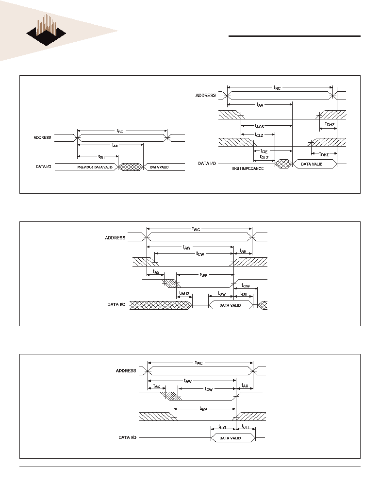
WS32K32-XHX
READ CYCLE 2, (CS# = OE# = V
IL
, WE# = V
IH
)
READ CYCLE 2 (WE# = V
IH
)
CS#
OE#
WRITE CYCLE 2, CS# CONTROLLED
CS#
WE#
WRITE CYCLE 2, CS# CONTROLLED
CS#
WE#
FIGURE 5 ≠ TIMING WAVEFORM - READ CYCLE
FIGURE 7 ≠ WRITE CYCLE - CS# CONTROLLED
FIGURE 6 ≠ WRITE CYCLE - WE# CONTROLLED