White Microelectronics ∑ (602) 437-1520 ∑ www.whiteedc.com
4
SRAM MODULES
1
WS128K32V-XXX
128Kx32 3.3V SRAM MULTICHIP PACKAGE
PRELIMINARY*
s 3.3 Volt Power Supply
s Low Power CMOS
s TTL Compatible Inputs and Outputs
s Built-in Decoupling Caps and Multiple Ground Pins for Low
Noise Operation
s Weight
WS128K32V-XG2TX - 8 grams typical
WS128K32V-XG1UX - 5 grams typical
WS128K32V-XH1X - 13 grams typical
*
This data sheet describes a product that is not fully qualified or
characterized and is subject ot change without notice.
** Commercial and Industrial temperature ranges only.
FEATURES
s Access Times of 15**, 17, 20, 25, 35ns
s Low Voltage Operation
s Packaging
∑ 66-pin, PGA Type, 1.075 inch square Hermetic Ceramic
HIP (Package 400)
∑ 68 lead, Hermetic CQFP (G2T), 22.4mm (0.880 inch) square
(Package 509), 4.57mm (0.180 inch) high. Designed to fit
JEDEC 68 lead 0.990" CQFJ footprint (Fig. 2)
∑ 68 lead, Hermetic CQFP (G1U), 23.8mm (0.940 inch)
square (Package 509), 3.56mm (0.140 inch) high.
s Organized as 128Kx32; User Configurable as 256Kx16 or
512Kx8
s Commercial, Industrial and Military Temperature Ranges
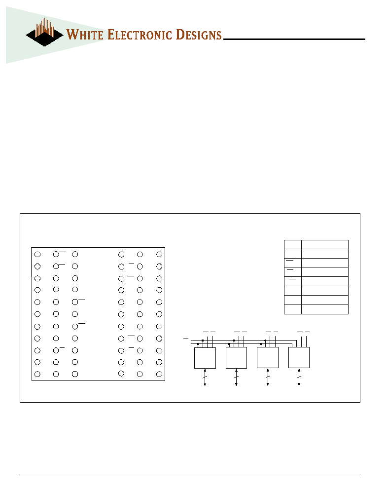
FIG. 1
PIN CONFIGURATION FOR WS128K32NV-XH1X
PIN DESCRIPTION
I/O
0-31
Data Inputs/Outputs
A
0-16
Address Inputs
WE
1-4
Write Enables
CS
1-4
Chip Selects
OE
Output Enable
V
CC
Power Supply
GND
Ground
NC
Not Connected
I/O
8
I/O
9
I/O
10
A
13
A
14
A
15
A
16
NC
I/O
0
I/O
1
I/O
2
WE
2
CS
2
GND
I/O
11
A
10
A
11
A
12
V
CC
CS
1
NC
I/O
3
I/O
15
I/O
14
I/O
13
I/O
12
OE
NC
WE
1
I/O
7
I/O
6
I/O
5
I/O
4
I/O
24
I/O
25
I/O
26
A
6
A
7
NC
A
8
A
9
I/O
16
I/O
17
I/O
18
V
CC
CS
4
WE
4
I/O
27
A
3
A
4
A
5
WE
3
CS
3
GND
I/O
19
I/O
31
I/O
30
I/O
29
I/O
28
A
0
A
1
A
2
I/O
23
I/O
22
I/O
21
I/O
20
11 22 33 44 55 66
1 12 23 34 45 56
TOP VIEW
BLOCK DIAGRAM
128K x 8
8
I / O
0 - 7
CS
1
128K x 8
8
I / O
8 - 1 5
2
128K x 8
8
I / O
1 6 - 2 3
3
128K x 8
8
I / O
2 4 - 3 1
4
A
0 - 1 6
O E
WE
CS
WE
CS
WE
CS
WE
1
2
3
4
April 2001 Rev. 2
2
White Microelectronics ∑ Phoenix, AZ ∑ (602) 437-1520
4
SRAM MODULES
WS128K32V-XXX
PIN DESCRIPTION
128K x 8
8
I / O
0 - 7
CS
1
128K x 8
8
I / O
8 - 1 5
2
128K x 8
8
I / O
1 6 - 2 3
3
128K x 8
8
I / O
2 4 - 3 1
4
A 0 - 1 6
O E
WE
CS
WE
CS
WE
CS
WE
1
2
3
4
BLOCK DIAGRAM
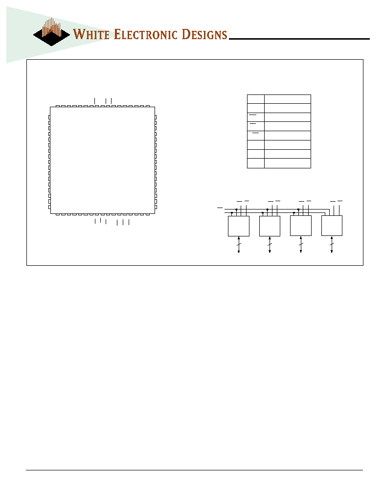
FIG. 2
PIN CONFIGURATION FOR WS128K32V-XG2TX AND WS128K32V-XG1UX
10
11
12
13
14
15
16
17
18
19
20
21
22
23
24
25
26
60
59
58
57
56
55
54
53
52
51
50
49
48
47
46
45
44
9 8 7 6 5 4 3 2 1 68 67 66 65 64 63 62 61
27 28 29 30 31 32 33 34 35 36 37 38 39 40 41 42 43
I/O
0
I/O
1
I/O
2
I/O
3
I/O
4
I/O
5
I/O
6
I/O
7
GND
I/O
8
I/O
9
I/O
10
I/O
11
I/O
12
I/O
13
I/O
14
I/O
15
V
CC
A
11
A
12
A
13
A
14
A
15
A
16
CS
1
OE
CS
2
NC
WE
2
WE
3
WE
4
NC
NC
NC
I/O
16
I/O
17
I/O
18
I/O
19
I/O
20
I/O
21
I/O
22
I/O
23
GND
I/O
24
I/O
25
I/O
26
I/O
27
I/O
28
I/O
29
I/O
30
I/O
31
NC
A
0
A
1
A
2
A
3
A
4
A
5
CS
3
GND
CS
4
WE
1
A
6
A
7
A
8
A
9
A
10
V
CC
TOP VIEW
I/O
0-31
Data Inputs/Outputs
A
0-16
Address Inputs
WE
1-4
Write Enables
CS
1-4
Chip Selects
OE
Output Enable
V
CC
Power Supply
GND
Ground
NC
Not Connected

White Microelectronics ∑ (602) 437-1520 ∑ www.whiteedc.com
4
SRAM MODULES
3
WS128K32V-XXX
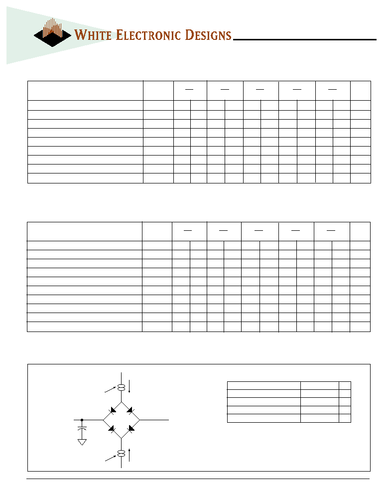
CAPACITANCE
(T
A
= +25
∞
C)
Parameter
Symbol
Conditions
Max
Unit
OE capacitance
C
OE
V
IN
= 0 V, f = 1.0 MHz
50
pF
WE
1-4
capacitance
C
WE
V
IN
= 0 V, f = 1.0 MHz
pF
HIP (PGA)
20
CQFP G2T/G1U
20
CS
1-4
capacitance
C
CS
V
IN
= 0 V, f = 1.0 MHz
20
pF
Data I/O capacitance
C
I/O
V
I/O
= 0 V, f = 1.0 MHz
20
pF
Address input capacitance
C
AD
V
IN
= 0 V, f = 1.0 MHz
50
pF
This parameter is guaranteed by design but not tested.
TRUTH TABLE
ABSOLUTE MAXIMUM RATINGS
Parameter
Symbol
Min
Max
Unit
Operating Temperature
T
A
-55
+125
∞
C
Storage Temperature
T
STG
-65
+150
∞
C
Signal Voltage Relative to GND
V
G
-0.5
4.6
V
Junction Temperature
T
J
150
∞
C
Supply Voltage
V
CC
-0.5
5.5
V
CS
OE
WE
Mode
Data I/O
Power
H
X
X
Standby
High Z
Standby
L
L
H
Read
Data Out
Active
L
X
L
Write
Data In
Active
L
H
H
Out Disable
High Z
Active
RECOMMENDED OPERATING CONDITIONS
Parameter
Symbol
Min
Max
Unit
Supply Voltage
V
CC
3.0
3.6
V
Input High Voltage
V
IH
2.2
V
CC
+ 0.3
V
Input Low Voltage
V
IL
-0.3
+0.8
V
DC CHARACTERISTICS
(V
CC
= 3.3V
±
0.3V, V
SS
= 0V, T
A
= -55
∞
C to +125
∞
C)
Parameter
Sym
Conditions
Units
Min
Max
Input Leakage Current
I
LI
V
IN
= GND to V
CC
10
µ
A
Output Leakage Current
I
LO
CS = V
IH
, OE = V
IH
, V
OUT
= GND to V
CC
10
µ
A
Operating Supply Current (x 32 Mode)
I
CC
x 32
CS = V
IL
, OE = V
IH
, f = 5MHz
500
mA
Standby Current
I
SB
CS = V
IH
, OE = V
IH
, f = 5MHz
32
mA
Output Low Voltage
V
OL
I
OL
= 8mA
0.4
V
Output High Voltage
V
OH
I
OH
= -4.0mA
2.4
V
4
White Microelectronics ∑ Phoenix, AZ ∑ (602) 437-1520
4
SRAM MODULES
WS128K32V-XXX
FIG. 3
AC TEST CIRCUIT
NOTES:
V
Z
is programmable from -2V to +7V.
I
OL
& I
OH
programmable from 0 to 16mA.
Tester Impedance Z
0
= 75
.
V
Z
is typically the midpoint of V
OH
and V
OL
.
I
OL
& I
OH
are adjusted to simulate a typical resistive load circuit.
ATE tester includes jig capacitance.
I
Current Source
D.U.T.
C = 50 pf
eff
I
OL
V
1.5V
(Bipolar Supply)
Z
Current Source
OH
AC TEST CONDITIONS
Parameter
Typ
Unit
Input Pulse Levels
V
IL
= 0, V
IH
= 3.0
V
Input Rise and Fall
5
ns
Input and Output Reference Level
1.5
V
Output Timing Reference Level
1.5
V
AC CHARACTERISTICS
(V
CC
= 3.3V, T
A
= -55
∞
C to +125
∞
C)
Parameter
Symbol
-15*
-17
-20
-25
-35
Units
Read Cycle
Min
Max
Min
Max
Min
Max
Min
Max
Min
Max
Read Cycle Time
t
RC
15
17
20
25
35
ns
Address Access Time
t
AA
15
17
20
25
35
ns
Output Hold from Address Change
t
OH
0
0
0
0
0
ns
Chip Select Access Time
t
ACS
15
17
20
25
35
ns
Output Enable to Output Valid
t
OE
10
11
12
15
20
ns
Chip Select to Output in Low Z
t
CLZ
1
5
5
5
5
5
ns
Output Enable to Output in Low Z
t
OLZ
1
5
5
5
5
5
ns
Chip Disable to Output in High Z
t
CHZ
1
8
9
10
12
15
ns
Output Disable to Output in High Z
t
OHZ
1
8
9
10
12
15
ns
1. This parameter is guaranteed by design but not tested.
* Commercial and Industrial only.
AC CHARACTERISTICS
(V
CC
= 3.3V, T
A
= -55
∞
C to +125
∞
C)
Parameter
Symbol
-15*
-17
-20
-25
-35
Units
Write Cycle
Min
Max
Min
Max
Min
Max
Min
Max
Min
Max
Write Cycle Time
t
WC
15
17
20
25
35
ns
Chip Select to End of Write
t
CW
13
14
15
20
30
ns
Address Valid to End of Write
t
AW
13
14
15
20
30
ns
Data Valid to End of Write
t
DW
10
11
12
15
18
ns
Write Pulse Width
t
WP
13
14
15
20
30
ns
Address Setup Time
t
AS
0
0
0
0
0
ns
Address Hold Time
t
AH
0
0
0
0
0
ns
Output Active from End of Write
t
OW
1
5
5
5
5
5
ns
Write Enable to Output in High Z
t
WHZ
1
8
9
10
10
15
ns
Data Hold Time
t
DH
0
0
0
0
0
ns
1. This parameter is guaranteed by design but not tested.
* Commercial and Industrial only.
White Microelectronics ∑ (602) 437-1520 ∑ www.whiteedc.com
4
SRAM MODULES
5
WS128K32V-XXX
WS32K32-XHX
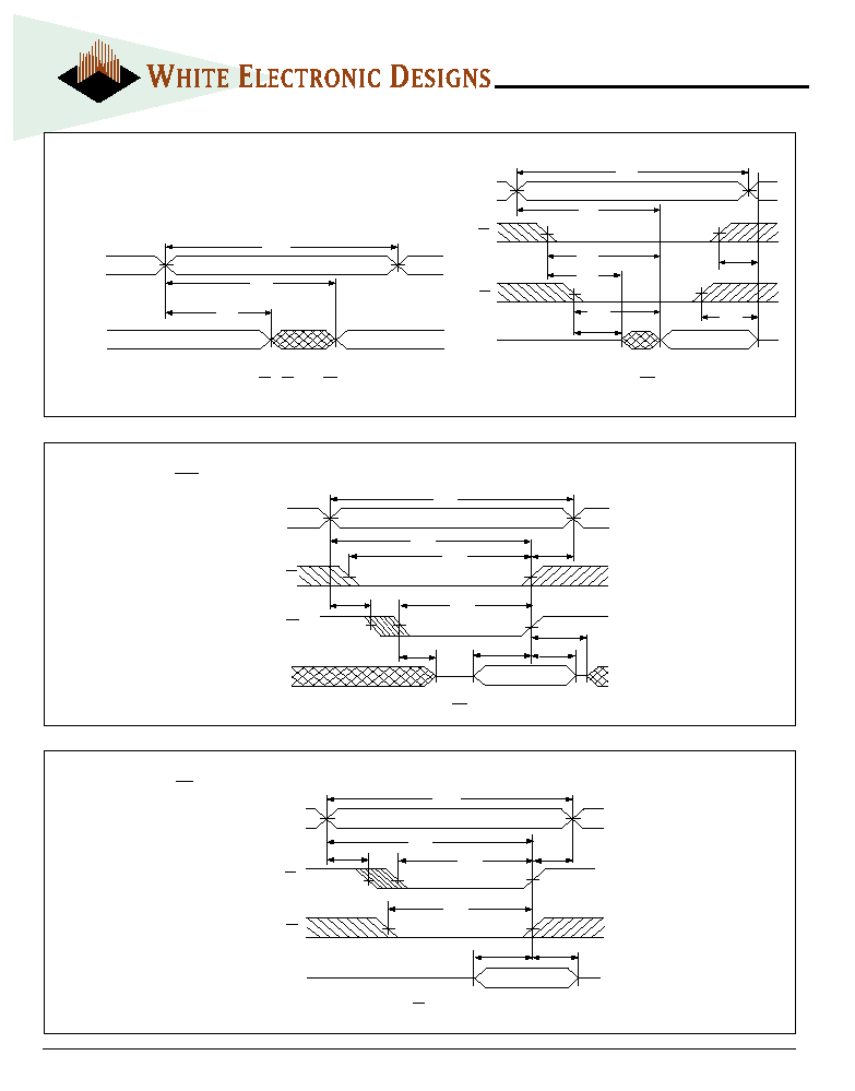
FIG. 4
TIMING WAVEFORM - READ CYCLE
FIG. 6
WRITE CYCLE - CS CONTROLLED
FIG. 5
WRITE CYCLE - WE CONTROLLED
ADDRESS
DATA I/O
WRITE CYCLE 1, WE CONTROLLED
t
AW
t
CW
t
AH
t
WP
t
DW
t
WHZ
t
AS
t
OW
t
DH
t
WC
DATA VALID
CS
WE
ADDRESS
DATA I/O
WRITE CYCLE 2, CS CONTROLLED
t
AW
t
AS
t
CW
t
AH
t
WP
t
DH
t
DW
t
WC
CS
WE
DATA VALID
ADDRESS
DATA I/O
READ CYCLE 2 (WE = V
IH
)
t
AA
t
ACS
t
OE
t
CLZ
t
OLZ
t
OHZ
t
RC
DATA VALID
HIGH IMPEDANCE
CS
OE
t
CHZ
ADDRESS
DATA I/O
READ CYCLE 1 (CS = OE = V
IL
, WE = V
IH
)
t
AA
t
OH
t
RC
DATA VALID
PREVIOUS DATA VALID