1
White Electronic Designs Corporation (602) 437-1520 www.whiteedc.com
White Electronic Designs
WS128K32V-XXX
128Kx32 3.3V SRAM MODULE
n Organized as 128Kx32; User Configurable as
256Kx16 or 512Kx8
n Commercial, Industrial and Military Temperature
Ranges
n 3.3 Volt Power Supply
n Low Power CMOS
n TTL Compatible Inputs and Outputs
n Built-in Decoupling Caps and Multiple Ground Pins
for Low Noise Operation
n Weight
WS128K32V-XG2UX - 8 grams typical
WS128K32NV-XH1X - 13 grams typical
WS128K32V-XG1UX
1
- 5 grams typical
WS128K32V-XG1TX - 5 grams typical
*This data sheet describes a product under development, not fully
characterized, and is subject to change without notice.
**Commercial and Industrial only.
Note 1: Package Not Recommended For New Design
FEATURES
n Access Times of 15**, 17, 20, 25, 35ns
n MIL-STD-883 Compliant Devices Available
n Low Voltage Operation
n Packaging
66-pin, PGA Type, 1.075 inch square Hermetic
Ceramic HIP (Package 400)
68 lead, Hermetic CQFP (G2U), 22.4mm (0.880
inch) square (Package 510), 3.56mm (0.140
inch) high.
68 lead, Hermetic CQFP (G1U)
1
, 23.9mm (0.940
inch) square (Package 519), 3.56mm (0.140
inch) high.
68 lead, Hermetic CQFP (G1T), 23.9mm (0.940
inch) square (Package 524), 4.06mm (0.160
inch) high.
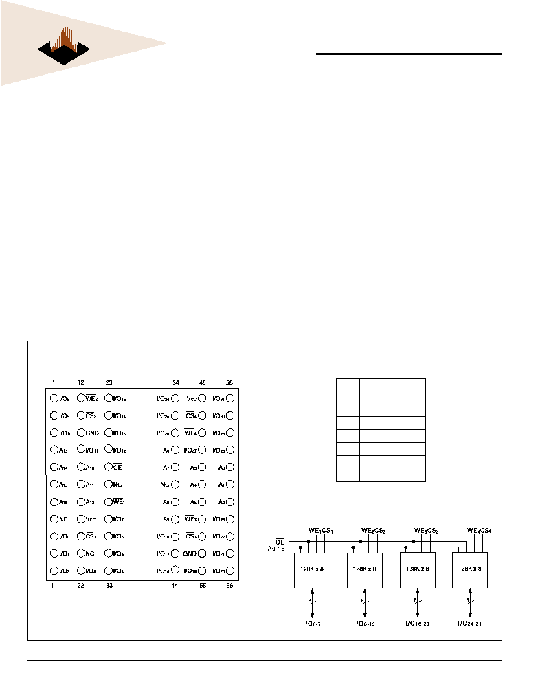
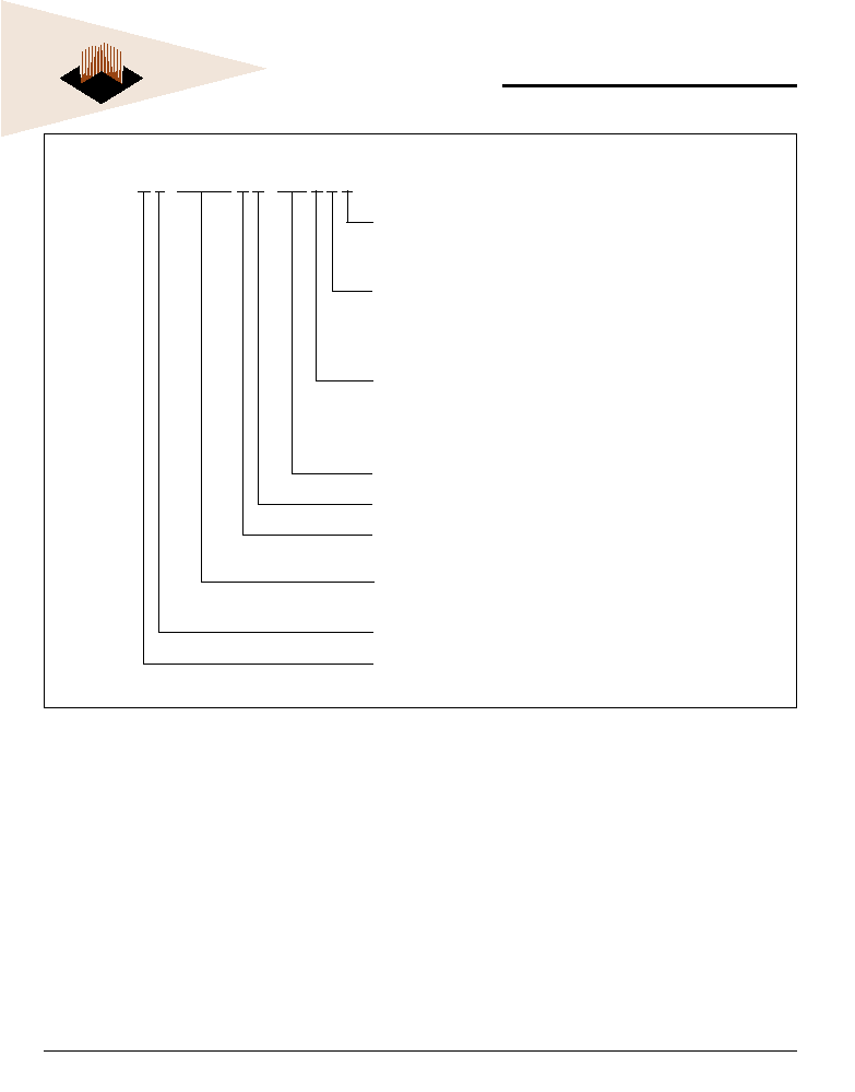
F
IG
. 1 P
IN
C
ONFIGURATION
F
OR
WS128K32NV-XH1X
P
IN
D
ESCRIPTION
I/O
0-31
Data Inputs/Outputs
A
0-16
Address Inputs
WE
1-4
Write Enables
CS
1-4
Chip Selects
OE
Output Enable
V
CC
Power Supply
GND
Ground
NC
Not Connected
T
OP
V
IEW
B
LOCK
D
IAGRAM
April 2003 Rev. 4
PRELIMINARY*
2
White Electronic Designs Corporation Phoenix AZ (602) 437-1520
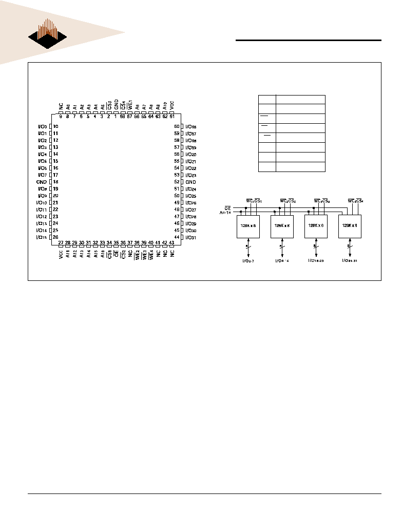
White Electronic Designs
WS128K32V-XXX
P
IN
D
ESCRIPTION
B
LOCK
D
IAGRAM
F
IG
. 2 P
IN
C
ONFIGURATION
F
OR
WS128K32V-XG1TX, WS128K32V-XG2UX
AND
WS128K32V-XG1UX
1
T
OP
V
IEW
I/O
0-31
Data Inputs/Outputs
A
0-16
Address Inputs
WE
1-4
Write Enables
CS
1-4
Chip Selects
OE
Output Enable
V
CC
Power Supply
GND
Ground
NC
Not Connected
Note 1: Package Not Recommended For New Design
3
White Electronic Designs Corporation (602) 437-1520 www.whiteedc.com
White Electronic Designs
WS128K32V-XXX
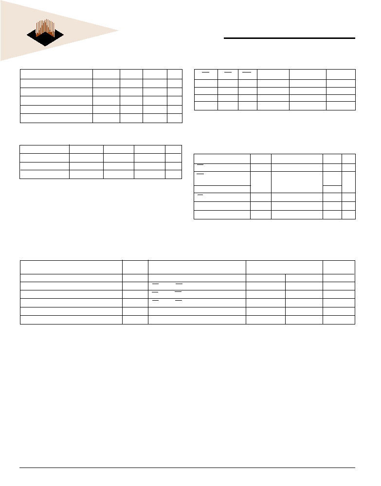
C
APACITANCE
(TA = +25∞C)
T
RUTH
T
ABLE
A
BSOLUTE
M
AXIMUM
R
ATINGS
Parameter
Symbol
Min
Max
Unit
Operating Temperature
T
A
-55
+125
∞C
Storage Temperature
T
STG
-65
+150
∞C
Signal Voltage Relative to GND
V
G
-0.5
4.6
V
Junction Temperature
T
J
150
∞C
Supply Voltage
V
CC
-0.5
5.5
V
CS
OE
WE
Mode
Data I/O
Power
H
X
X
Standby
High Z
Standby
L
L
H
Read
Data Out
Active
L
X
L
Write
Data In
Active
L
H
H
Out Disable
High Z
Active
R
ECOMMENDED
O
PERATING
C
ONDITIONS
Parameter
Symbol
Min
Max
Unit
Supply Voltage
V
CC
3.0
3.6
V
Input High Voltage
V
IH
2.2
V
CC
+ 0.3
V
Input Low Voltage
V
IL
-0.3
+0.8
V
DC C
HARACTERISTICS
(V
CC
= 3.3V ±0.3V, V
SS
= 0V, T
A
= -55∞C
TO
+125∞C)
Parameter
Sym
Conditions
Units
Min
Max
Input Leakage Current
I
LI
V
IN
= GND to V
CC
10
µA
Output Leakage Current
I
LO
CS = V
IH
, OE = V
IH
, V
OUT
= GND to V
CC
10
µA
Operating Supply Current (x 32 Mode)
I
CC
x 32
CS = V
IL
, OE = V
IH
, f = 5MHz
500
mA
Standby Current
I
SB
CS = V
IH
, OE = V
IH
, f = 5MHz
32
mA
Output Low Voltage
V
OL
I
OL
= 8mA
0.4
V
Output High Voltage
V
OH
I
OH
= -4.0mA
2.4
V
Parameter
Symbol
Conditions
Max
Unit
OE capacitance
C
OE
V
IN
= 0 V, f = 1.0 MHz
50
pF
WE
1-4
capacitance
C
WE
V
IN
= 0 V, f = 1.0 MHz
pF
HIP (PGA)
20
CQFP G2U/G1U/G1T
20
CS
1-4
capacitance
C
CS
V
IN
= 0 V, f = 1.0 MHz
20
pF
Data I/O capacitance
C
I/O
V
I/O
= 0 V, f = 1.0 MHz
20
pF
Address input capacitance
C
AD
V
IN
= 0 V, f = 1.0 MHz
50
pF
This parameter is guaranteed by design but not tested.

4
White Electronic Designs Corporation Phoenix AZ (602) 437-1520
White Electronic Designs
WS128K32V-XXX
F
IG
. 3 AC T
EST
C
IRCUIT
Notes:
V
Z
is programmable from -2V to +7V.
I
OL
& I
OH
programmable from 0 to 16mA.
Tester Impedance Z
0
= 75W.
V
Z
is typically the midpoint of V
OH
and V
OL
.
I
OL
& I
OH
are adjusted to simulate a typical resistive load circuit.
ATE tester includes jig capacitance.
AC T
EST
C
ONDITIONS
Parameter
Typ
Unit
Input Pulse Levels
V
IL
= 0, V
IH
= 3.0
V
Input Rise and Fall
5
ns
Input and Output Reference Level
1.5
V
Output Timing Reference Level
1.5
V
AC C
HARACTERISTICS
(V
CC
= 3.3V, T
A
= -55∞C
TO
+125∞C)
Parameter
Symbol
-15*
-17
-20
-25
-35
Units
Read Cycle
Min
Max
Min
Max
Min
Max
Min
Max
Min
Max
Read Cycle Time
t
RC
15
17
20
25
35
n s
Address Access Time
t
A A
15
17
20
25
35
n s
Output Hold from Address Change
t
OH
0
0
0
0
0
n s
Chip Select Access Time
t
A C S
15
17
20
25
35
n s
Output Enable to Output Valid
t
OE
10
11
12
15
20
n s
Chip Select to Output in Low Z
t
CLZ
1
5
5
5
5
5
n s
Output Enable to Output in Low Z
t
OLZ
1
5
5
5
5
5
n s
Chip Disable to Output in High Z
t
CHZ
1
8
9
10
12
15
n s
Output Disable to Output in High Z
t
OHZ
1
8
9
10
12
15
n s
AC C
HARACTERISTICS
(V
CC
= 3.3V, T
A
= -55∞C
TO
+125∞C)
Parameter
Symbol
-15*
-17
-20
-25
-35
Units
Write Cycle
Min
Max
Min
Max
Min
Max
Min
Max
Min
Max
Write Cycle Time
t
WC
15
17
20
25
35
n s
Chip Select to End of Write
t
CW
13
14
15
20
30
n s
Address Valid to End of Write
t
AW
13
14
15
20
30
n s
Data Valid to End of Write
t
DW
10
11
12
15
18
n s
Write Pulse Width
t
WP
13
14
15
20
30
n s
Address Setup Time
t
A S
0
0
0
0
0
n s
Address Hold Time
t
A H
0
0
0
0
0
n s
Output Active from End of Write
t
OW
1
5
5
5
5
5
n s
Write Enable to Output in High Z
t
WHZ
1
8
9
10
10
15
n s
Data Hold Time
t
DH
0
0
0
0
0
n s
1. This parameter is guaranteed by design but not tested.
* Commercial and Industrial only.
1. This parameter is guaranteed by design but not tested.
* Commercial and Industrial only.
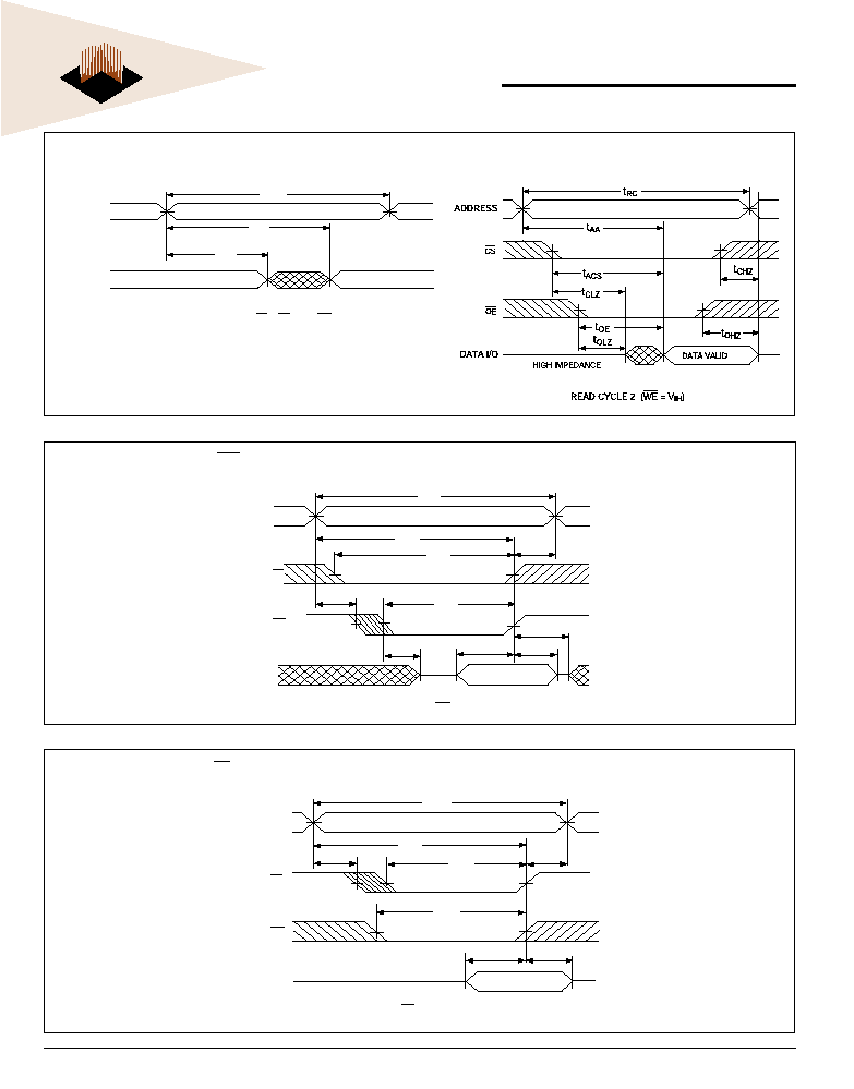
5
White Electronic Designs Corporation (602) 437-1520 www.whiteedc.com
White Electronic Designs
WS128K32V-XXX
WS32K32-XHX
F
IG
. 4 T
IMING
W
AVEFORM
- R
EAD
C
YCLE
F
IG
. 6 W
RITE
C
YCLE
- CS C
ONTROLLED
F
IG
. 5 W
RITE
C
YCLE
- WE C
ONTROLLED
ADDRESS
DATA I/O
READ CYCLE 1 (CS = OE = V
IL
, WE = V
IH
)
t
AA
t
OH
t
RC
DATA VALID
PREVIOUS DATA VALID
ADDRESS
DATA I/O
WRITE CYCLE 1, WE CONTROLLED
t
AW
t
CW
t
AH
t
WP
t
DW
t
WHZ
t
AS
t
OW
t
DH
t
WC
DATA VALID
CS
WE
ADDRESS
DATA I/O
WRITE CYCLE 2, CS CONTROLLED
t
AW
t
AS
t
CW
t
AH
t
WP
t
DH
t
DW
t
WC
CS
WE
DATA VALID

6
White Electronic Designs Corporation Phoenix AZ (602) 437-1520
White Electronic Designs
WS128K32V-XXX
P
ACKAGE
400: 66 P
IN
, PGA T
YPE
, C
ERAMIC
H
EX
-I
N
-L
INE
P
ACKAGE
, H
IP
(H1)
ALL LINEAR DIMENSIONS ARE MILLIMETERS AND PARENTHETICALLY IN INCHES

7
White Electronic Designs Corporation (602) 437-1520 www.whiteedc.com
White Electronic Designs
WS128K32V-XXX
P
ACKAGE
510: 68 L
EAD
, L
OW
P
ROFILE
C
ERAMIC
Q
UAD
F
LAT
P
ACK
, CQFP (G2U)
ALL LINEAR DIMENSIONS ARE MILLIMETERS AND PARENTHETICALLY IN INCHES
P
ACKAGE
519: 68 L
EAD
, C
ERAMIC
Q
UAD
F
LAT
P
ACK
, CQFP (G1U)
1
ALL LINEAR DIMENSIONS ARE MILLIMETERS AND PARENTHETICALLY IN INCHES
Note 1: Package Not Recommended For New Design

8
White Electronic Designs Corporation Phoenix AZ (602) 437-1520
White Electronic Designs
WS128K32V-XXX
P
ACKAGE
524: 68 L
EAD
, C
ERAMIC
Q
UAD
F
LAT
P
ACK
, L
OW
P
ROFILE
CQFP (G1T)
ALL LINEAR DIMENSIONS ARE MILLIMETERS AND PARENTHETICALLY IN INCHES
25.27 (0.995)
± 0.13 (0.005) SQ
23.88 (0.940)
± 0.25 (0.010) SQ
0.38 (0.015)
± 0.05 (0.002)
20.3 (0.800) REF
1.27 (0.050)
4.06 (0.160) MAX
0.25 (0.010) MAX
SEE DETAIL "A"
0.84 (0.033) REF
DETAIL A
0.83 (0.033)
± 0.32 (0.013)
9
White Electronic Designs Corporation (602) 437-1520 www.whiteedc.com
White Electronic Designs
WS128K32V-XXX
O
RDERING
I
NFORMATION
LEAD FINISH:
Blank = Gold plated leads
A = Solder dip leads
DEVICE GRADE:
M = Military Screened -55∞C to +125∞C
I = Industrial
-40∞C to +85∞C
C = Commercial
0∞C to +70∞C
PACKAGE TYPE:
H1 = Ceramic Hex-In-line Package, HIP (Package 400)
G2U = 22.4mm Ceramic Quad Flat Pack, Low Profile CQFP (Package 510)
G1U
1
= 23.9mm Ceramic Quad Flat Pack, Low Profile CQFP (Package 519)
G1T = 23.9mm Ceramic Quad Flat Pack, Low Profile CQFP (Package 524)
ACCESS TIME (ns)
LOW VOLTAGE SUPPLY 3.3V ± 10%
IMPROVEMENT MARK:
N = No Connect at pins 8, 21, 28, 39 in HIP for upgrade. (H1 only)
ORGANIZATION, 128Kx32
User configurable as 256Kx16 or 512Kx8
SRAM
WHITE ELECTRONIC DESIGNS CORP.
W S 128K 32 X V - XXX X X X
Note 1: Package Not Recommended For New Design