1
White Electronic Designs Corporation (602) 437-1520 www.whiteedc.com
White Electronic Designs
WS1M32-XXX
1Mx32 SRAM MODULE
FEATURES
Access Times of 17, 20, 25ns
Packaging
84 lead, 28mm CQFP, (Package 511)
66 pin PGA Type, 1.385" sq., Hermetic Ce-
ramic HIP
(Package 402)*
Organized as two banks of 512Kx32, User
Configurable as 2Mx16 or 4Mx8
* Package to be developed.
Commercial, Industrial and Military Temperature
Ranges
TTL Compatible Inputs and Outputs
5 Volt Power Supply
Low Power CMOS
Built-in Decoupling Caps and Multiple Ground
Pins for Low Noise Operation
Weight
WS1M32-XH2X* - 13 grams (typical)
WS1M32-XG3X - 20 grams (typical)
July 2002 Rev. 4
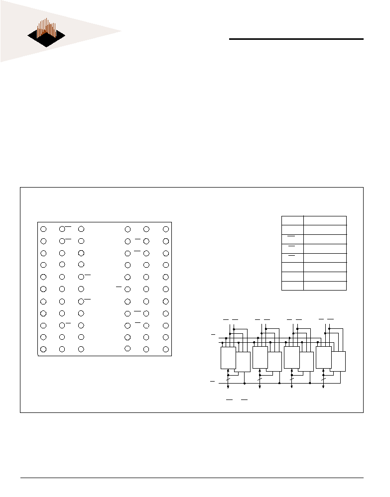
PIN DESCRIPTION
PIN CONFIGURATION FOR WS1M32-XH2X*
I/O
8
I/O
9
I/O
10
A
13
A
14
A
15
A
16
A
17
I/O
0
I/O
1
I/O
2
WE
2
OE
2
GND
I/O
11
A
10
A
11
A
12
V
CC
CS
1
NC
I/O
3
I/O
15
I/O
14
I/O
13
I/O
12
OE
1
A
18
WE
1
I/O
7
I/O
6
I/O
5
I/O
4
I/O
24
I/O
25
I/O
26
A
6
A
7
CS
2
A
8
A
9
I/O
16
I/O
17
I/O
18
V
CC
OE
4
WE
4
I/O
27
A
3
A
4
A
5
WE
3
OE
3
GND
I/O
19
I/O
31
I/O
30
I/O
29
I/O
28
A
0
A
1
A
2
I/O
23
I/O
22
I/O
21
I/O
20
11 22 33 44 55 66
1 12 23 34 45 56
BLOCK DIAGRAM
TOP VIEW
I/O
0
-
31
Data Inputs/Outputs
A
0-18
Address Inputs
WE
1-4
Write Enables
CS
1-2
Chip Selects
OE
1-4
Output Enable
V
CC
Power Supply
GND
Ground
NC
Not Connected
8
I/O
0-7
CS
1
I/O
8-15
CS
2
I/O
16-23
I/O
24-31
A
0-18
WE
1
8
2M x 8
8
512K x 8
8
512K x 8
2M x 8
512K x 8
512K x 8
2M x 8
512K x 8
512K x 8
2M x 8
512K x 8
512K x 8
OE
1
WE
2
OE
2
WE
3
OE
3
WE
4
OE
4
NOTE: CS
1
& CS
2
are used as bank select

2
White Electronic Designs Corporation Phoenix AZ (602) 437-1520
White Electronic Designs
WS1M32-XXX
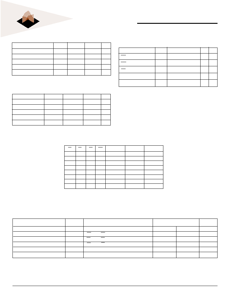
PIN CONFIGURATION FOR WS1M32-XG3X
TOP VIEW
BLOCK DIAGRAM
8
I/O
0-7
CS
1
I/O
8-15
CS
2
I/O
16-23
I/O
24-31
A
0-18
WE
1
8
2M x 8
8
512K x 8
8
512K x 8
2M x 8
512K x 8
512K x 8
2M x 8
512K x 8
512K x 8
2M x 8
512K x 8
512K x 8
OE
1
WE
2
OE
2
WE
3
OE
3
WE
4
OE
4
NOTE: CS
1
& CS
2
are used as bank select
1.146"
12
13
14
15
16
17
18
19
20
21
22
23
24
25
26
27
28
29
30
31
32
74
73
72
71
70
69
68
67
66
65
64
63
62
61
60
59
58
57
56
55
54
9
V
CC
A
0
A
1
A
2
A
3
A
4
A
5
A
6
OE
1
OE
2
OE
3
OE
4
NC
A
7
A
8
A
9
A
10
A
11
A
12
A
13
GND
V
CC
I/O
0
I/O
1
I/O
2
I/O
3
I/O
4
I/O
5
I/O
6
I/O
7
CS
1
NC
CS
2
I/O
8
I/O
9
I/O
10
I/O
11
I/O
12
I/O
13
I/O
14
I/O
15
GND
GND
NC
NC
NC
NC
NC
NC
NC
NC
WE
4
WE
3
WE
2
WE
1
NC
NC
A
18
A
17
A
16
A
15
A
14
V
CC
GND
I/O
31
I/O
30
I/O
29
I/O
28
I/O
27
I/O
26
I/O
25
I/O
24
NC
NC
NC
I/O
23
I/O
22
I/O
21
I/O
20
I/O
19
I/O
18
I/O
17
I/O
16
V
CC
8 7 6 5 4 3
1 84 83 82 81 80 79 78 77
2
37
38 39 40 41 42 43
45 46 47 48 49 50 51 52 53
44
76 75
11
10
33
34 35 36
The WEDC 84 lead G3 CQFP fills
the same fit and function as the
JEDEC 84 lead CQFJ or 84
PLCC. But the G3 has the TCE
and lead inspection advantage of
the CQFP form.
PIN DESCRIPTION
I/O
0-31
Data Inputs/Outputs
A
0-18
Address Inputs
WE
1-4
Write Enables
CS
1-2
Chip Selects
OE
1-4
Output Enables
V
CC
Power Supply
GND
Ground
NC
Not Connected
3
White Electronic Designs Corporation (602) 437-1520 www.whiteedc.com
White Electronic Designs
WS1M32-XXX
Parameter
Symbol
Conditions
Max Unit
OE
1-4
capacitance
C
OE
V
IN
= 0 V, f = 1.0 MHz
30
pF
WE
1-4
capacitance
C
WE
V
IN
= 0 V, f = 1.0 MHz
30
pF
CS
1-2
capacitance
C
CS
V
IN
= 0 V, f = 1.0 MHz 30
pF
Data I/O capacitance
C
I/O
V
I/O
= 0 V, f = 1.0 MHz 30
pF
Address input capacitance C
AD
V
IN
= 0 V, f = 1.0 MHz 75
pF
This parameter is guaranteed by design but not tested.
Parameter
Symbol
Min
Max
Unit
Operating Temperature
T
A
-55
+125
�C
Storage Temperature
T
STG
-65
+150
�C
Signal Voltage Relative to GND
V
G
-0.5
Vcc + 0.5
V
Junction Temperature
T
J
150
�C
Supply Voltage
V
CC
-0.5
7.0
V
ABSOLUTE MAXIMUM RATINGS
CAPACITANCE
(T
A
= +25�C)
TRUTH TABLE
CS
1
CS
2
OE
WE
Mode
Data I/O
Power
H
H
X
X
Standby
High Z
Standby
L
H
L
H
Read
Data Out
Active
L
H
H
H
Out Disable
High Z
Active
L
H
X
L
Write
Data In
Active
H
L
L
H
Read
Data Out
Active
H
L
H
H
Out Disable
High Z
Active
H
L
X
L
Write
Data In
Active
L
L
X
X
Invalid State Invalid State Invalid State
Parameter
Symbol
Conditions
Units
Min
Max
Input Leakage Current
I
LI
V
CC
= 5.5, V
IN
= G
ND
to V
CC
10
�A
Output Leakage Current
I
LO
CS = V
IH
, OE = V
IH
, V
OUT
= GND to V
CC
10
�A
Operating Supply Current x 32 Mode
I
CC x 32
CS = V
IL
, OE = V
IH
, f = 5MHz, Vcc = 5.5
720
mA
Standby Current
I
SB
CS = V
IH
, OE = V
IH
, f = 5MHz, Vcc = 5.5
120
mA
Output Low Voltage
V
OL
I
OL
= 8mA, Vcc = 4.5
0.4
V
Output High Voltage
V
OH
I
OH
= -4.0mA, Vcc = 4.5
2.4
V
NOTE: DC test conditions: V
IH
= V
CC
-0.3V, V
IL
= 0.3V
DC CHARACTERISTICS
(V
CC
= 5.0V, GND = 0V, T
A
= -55�C to +125�C)
RECOMMENDED OPERATING CONDITIONS
Parameter
Symbol
Min
Max
Unit
Supply Voltage
V
CC
4.5
5.5
V
Input High Voltage
V
IH
2.2
V
CC
+ 0.3
V
Input Low Voltage
V
IL
-0.5
+0.8
V
Operating Temp (Mil)
T
A
-55
+125
�C
Operating Temp (Ind.)
T
A
-40
+85
�C
4
White Electronic Designs Corporation Phoenix AZ (602) 437-1520
White Electronic Designs
WS1M32-XXX
Parameter
Symbol
-17
-20
-25
Units
Read Cycle
Min
Max
Min
Max
Min
Max
Read Cycle Time
t
RC
17
20
25
ns
Address Access Time
t
AA
17
20
25
ns
Output Hold from Address Change
t
OH
0
0
0
ns
Chip Select Access Time
t
ACS
17
20
25
ns
Output Enable to Output Valid
t
OE
10
10
12
ns
Chip Select to Output in Low Z
t
CLZ
1
2
2
2
ns
Output Enable to Output in Low Z
t
OLZ
1
0
0
0
ns
Chip Disable to Output in High Z
t
CHZ
1
12
12
12
ns
Output Disable to Output in High Z
t
OHZ
1
12
12
12
ns
1. This parameter is guaranteed by design but not tested.
AC CHARACTERISTICS
(V
CC
= 5.0V, GND = 0V, T
A
= -55�C to +125�C)
NOTES:
V
Z
is programmable from -2V to +7V.
I
OL
& I
OH
programmable from 0 to 16mA.
Tester Impedance Z0 = 75W.
V
Z
is typically the midpoint of V
OH
and V
OL
.
I
OL
& I
OH
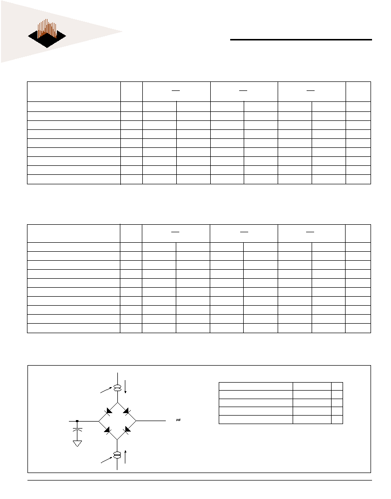
are adjusted to simulate a typical resistive load circuit.
ATE tester includes jig capacitance.
I
Current Source
D.U.T.
C = 50 pf
eff
I
OL
V 1.5V
(Bipolar Supply)
Z
Current Source
OH
AC CHARACTERISTICS
(V
CC
= 5.0V, GND = 0V, T
A
= -55�C to +125�C)
AC TEST CONDITIONS
Parameter
Typ
Unit
Input Pulse Levels
V
IL
= 0, V
IH
= 3.0 V
Input Rise and Fall
5
ns
Input and Output Reference Level
1.5
V
Output Timing Reference Level
1.5
V
Parameter
Symbol
-17
-20
-25
Units
Write Cycle
Min
Max
Min
Max
Min
Max
Write Cycle Time
t
WC
17
20
25
ns
Chip Select to End of Write
t
CW
15
15
17
ns
Address Valid to End of Write
t
AW
15
15
17
ns
Data Valid to End of Write
t
DW
11
12
13
ns
Write Pulse Width
t
WP
15
15
17
ns
Address Setup Time
t
AS
2
2
2
ns
Address Hold Time
t
AH
0
0
0
ns
Output Active from End of Write
t
OW
1
2
3
4
ns
Write Enable to Output in High Z t
WHZ
1
9
11
13
ns
Data Hold Time
t
DH
0
0
0
ns
1. This parameter is guaranteed by design but not tested.
AC TEST CIRCUIT
5
White Electronic Designs Corporation (602) 437-1520 www.whiteedc.com
White Electronic Designs
WS1M32-XXX
WS32K32-XHX
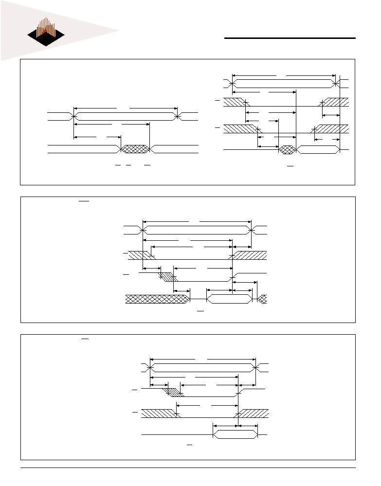
TIMING WAVEFORM - READ CYCLE
WRITE CYCLE - CS CONTROLLED
WRITE CYCLE - WE CONTROLLED
ADDRESS
DATA I/O
WRITE CYCLE 2, CS CONTROLLED
t
AW
t
AS
t
CW
t
AH
t
WP
t
DH
t
DW
t
WC
CS
WE
DATA VALID
ADDRESS
DATA I/O
READ CYCLE 2 (WE = V
IH
)
t
AA
t
ACS
t
OE
t
CLZ
t
OLZ
t
OHZ
t
RC
DATA VALID
HIGH IMPEDANCE
CS
OE
t
CHZ
ADDRESS
DATA I/O
READ CYCLE 1 (CS = OE = V
IL
, WE = V
IH
)
t
AA
t
OH
t
RC
DATA VALID
PREVIOUS DATA VALID
ADDRESS
DATA I/O
WRITE CYCLE 1, WE CONTROLLED
t
AW
t
CW
t
AH
t
WP
t
DW
t
WHZ
t
AS
t
OW
t
DH
t
WC
DATA VALID
CS
WE