 | –≠–ª–µ–∫—Ç—Ä–æ–Ω–Ω—ã–π –∫–æ–º–ø–æ–Ω–µ–Ω—Ç: WS1M8-XXX | –°–∫–∞—á–∞—Ç—å:  PDF PDF  ZIP ZIP |

1
White Electronic Designs Corporation ∑ (602) 437-1520 ∑ www.wedc.com
White Electronic Designs
WS1M8-XXX
July 2004
Rev. 5
White Electronic Designs Corp. reserves the right to change products or specifi cations without notice.
2x512Kx8 DUALITHICTM SRAM
FEATURES
Access Times 17, 20, 25, 35, 45, 55ns
Revolutionary, Center Power/Ground Pinout
Packaging:
∑ 32 pin, Her
met ic Ceramic DIP (Package 300)
∑ 36 lead Ceramic SOJ (Package 100)
∑ 36 lead Ceramic Flatpack (Package 226)
36
CSOJ
36
FLATPACK
TOP VIEW
1
2
3
4
5
6
7
8
9
10
11
12
13
14
15
16
17
18
36
35
34
33
32
31
30
29
28
27
26
25
24
23
22
21
20
19
A0
A1
A2
A3
A4
CS1#
I/O0
I/O1
V
CC
GND
I/O2
I/O3
WE#
A5
A6
A7
A8
A9
NC
A18
A17
A16
A15
OE#
I/O7
I/O6
GND
V
CC
I/O5
I/O4
A14
A13
A12
A11
A10
CS2#
Block Diagram
512K x 8
512K x 8
A 0 - 1 8
O E #
W E #
C S 1 #
C S 2 #
I / O 0 - 7
(1)
(1)
PIN CONFIGURATION FOR WS1M8-XDJX
AND WS1M8-XFX
Pin Description
A0-18
Address Inputs
I/O0-7
Data Input/Output
CS1-2#
Chip Selects
OE#
Output Enable
WE#
Write Enable
V
CC
+5.0V Power
GND
Ground
NOTE:
1. CS1# and CS2# are used to select the lower and upper 512Kx8 of the device. CS1# and CS2# must not be enabled at the same time.
Organized as two banks of 512Kx8
Commercial, Industrial and Military Temperature Ranges
5 Volt Power Supply
Low Power CMOS
TTL Compatible Inputs and Outputs
PIN CONFIGURATION FOR WS1M8-XCX
32
DIP
TOP VIEW
512K x 8
512K x 8
A 0 - 1 8
W E #
C S
1 #
C S
2 #
I / O 0 - 7
(1)
(1)
1
2
3
4
5
6
7
8
9
10
11
12
13
14
15
16
32
31
30
29
28
27
26
25
24
23
22
21
20
19
18
17
A18
A16
A14
A12
A7
A6
A5
A4
A3
A2
A1
A0
I/O0
I/O1
I/O2
GND
V
CC
A15
A17
WE#
A13
A8
A9
A11
CS2#
A10
CS1#
I/O7
I/O6
I/O5
I/O4
I/O3
Pin Description
A0-18
Address Inputs
I/O0-7
Data Input/Output
CS1-2#
Chip Selects
WE#
Write Enable
V
CC
+5.0V Power
GND
Ground
Block Diagram
2
White Electronic Designs Corporation ∑ (602) 437-1520 ∑ www.wedc.com
White Electronic Designs
WS1M8-XXX
July 2004
Rev. 5
White Electronic Designs Corp. reserves the right to change products or specifi cations without notice.
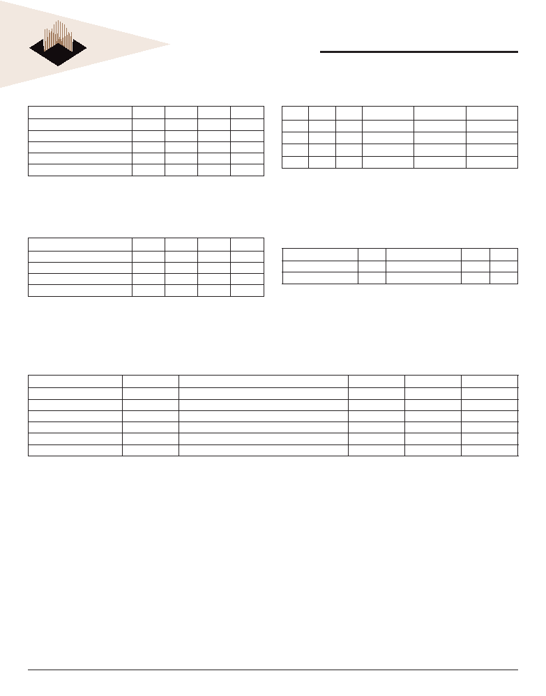
ABSOLUTE MAXIMUM RATINGS
Parameter
Symbol
Min
Max
Unit
Operating Temperature
T
A
-55 +125
∞C
Storage Temperature
T
STG
-65
+150
∞C
Signal Voltage Relative to GND
V
G
-0.5
V
CC
+0.5
V
Junction Temperature
T
J
150
∞C
Supply Voltage
V
CC
-0.5
7.0
V
TRUTH TABLE
CS#
OE#
WE#
Mode
Data I/O
Power
H
X
X
Standby
High Z
Standby
L
L
H
Read
Data Out
Active
L
X
L
Write
Data In
Active
L
H
H
Out Disable
High Z
Active
NOTE: OE# is internally tied to the GND and not accessible on the WS1M8-XCXX.
RECOMMENDED OPERATING CONDITIONS
Parameter
Symbol
Min
Max
Unit
Supply Voltage
V
CC
4.5
5.5
V
Input High Voltage
V
IH
2.2
V
CC
+ 0.3
V
Input Low Voltage
V
IL
-0.3
+0.8
V
Operating Temp. (Mil.)
T
A
-55
+125
∞C
CAPACITANCE
T
A
= +25∞C
Parameter
Symbol
Condition
Max
Unit
Input capacitance
C
IN
V
IN
= 0V, f = 1.0MHz
20
pF
Output capicitance
C
OUT
V
OUT
= 0V, f = 1.0MHz
20
pF
This parameter is guaranteed by design but not tested.
DC CHARACTERISTICS
V
CC
= 5.0V, V
SS
= 0V, -55∞C T
A
+125∞C
Parameter
Sym
Conditions
Min
Max
Units
Input Leakage Current
I
LI
V
CC
= 5.5, V
IN
= GND to V
CC
10
µA
Output Leakage Current
I
LO
1
CS# = V
IH
, OE# = V
IH
, V
OUT
= GND to V
CC
10
µA
Operating Supply Current
I
CC
1
CS# = V
IL
, OE# = V
IH
, f = 5MHz, V
CC
= 5.5
180
mA
Standby Current
I
SB
1
CS# = V
IH
, OE# = V
IH
, f = 5MHz, V
CC
= 5.5
40
mA
Output Low Voltage
V
OL
I
OL
= 6mA
0.4
V
Output High Voltage
V
OH
I
OH
= -4.0mA
2.4
V
NOTE: DC test conditions: V
IH
= V
CC
-0.3V , V
IL
= 0.3V
1. OE# is internally tied to the GND and not accessible on the WS1M8-XCXX.

3
White Electronic Designs Corporation ∑ (602) 437-1520 ∑ www.wedc.com
White Electronic Designs
WS1M8-XXX
July 2004
Rev. 5
White Electronic Designs Corp. reserves the right to change products or specifi cations without notice.
I
Current Source
D.U.T.
C = 50 pf
eff
I
OL
V
1.5V
(Bipolar Supply)
Z
Current Source
OH
AC TEST CIRCUIT
AC TEST CONDITIONS
Parameter
Typ
Unit
Input Pulse Levels
VIL = 0, VIH = 3.0
V
Input Rise and Fall
5
ns
Input and Output Reference Level
1.5
V
Output Timing Reference Level
1.5
V
Notes:
V
Z
is programmable from -2V to +7V.
I
OL
& I
OH
programmable from 0 to 16mA.
Tester Impedance Z0 = 75 .
V
Z
is typically the midpoint of V
OH
and V
OL
.
I
OL
& I
OH
are adjusted to simulate a typical resistive load cir cuit.
ATE tester includes jig capacitance.
AC CHARACTERISTICS
V
CC
= 5.0V, V
SS
= 0V, -55∞C T
A
+125∞C
Parameter
Read Cycle
Symbol
-17
-20
-25
-35
-45
-55
Units
Min
Max
Min
Max
Min
Max
Min
Max
Min
Max
Min
Max
Read Cycle Time
t
RC
17
20
25
35
45
55
ns
Address Access Time
t
AA
17
20
25
35
45
55
ns
Output Hold from Address Change
t
OH
0
0
0
0
0
0
ns
Chip Select Access Time
t
ACS
17
20
25
35
45
55
ns
Output Enable to Output Valid
t
OE
2
9
10
12
25
25
25
ns
Chip Select to Output in Low Z
t
CLZ
1
2
2
2
4
4
4
ns
Output Enable to Output in Low Z
t
OLZ
2
0
0
0
0
0
0
ns
Chip Disable to Output in High Z
t
CHZ
1
9
10
12
15
20
20
ns
Output Disable to Output in High Z
t
OHZ
2
9
10
12
15
20
20
ns
1. This parameter is guaranteed by design but not tested.
2. OE# is internally tied to the GND and not accessible on the WS1M8-XCXX.
AC CHARACTERISTICS
V
CC
= 5.0V, V
SS
= 0V, -55∞C T
A
+125∞C
Parameter
Write Cycle
Symbol
-17
-20
-25
-35
-45
-55
Units
Write Cycle Time
t
WC
17
20
25
35
45
55
ns
Chip Select to End of Write
t
CW
14
14
15
25
35
50
ns
Address Valid to End of Write
t
AW
14
14
15
25
35
50
ns
Data Valid to End of Write
t
DW
9
10
10
20
25
25
ns
Write Pulse Width
t
WP
14
14
15
25
35
40
ns
Address Setup Time
t
AS
0
0
0
0
0
0
ns
Address Hold Time
t
AH
0
0
0
0
5
5
ns
Output Active from End of Write
t
OW
1
2
3
4
4
5
5
ns
Write Enable to Output in High Z
t
WHZ
1
9
9
10
15
15
25
ns
Data Hold Time
t
DH
0
0
0
0
0
0
ns
1. This parameter is guaranteed by design but not tested.

4
White Electronic Designs Corporation ∑ (602) 437-1520 ∑ www.wedc.com
White Electronic Designs
WS1M8-XXX
July 2004
Rev. 5
White Electronic Designs Corp. reserves the right to change products or specifi cations without notice.
TIMING WAVEFORM ≠ READ CYCLE
WRITE CYCLE ≠ CS# CONTROLLED
ADDRESS
DATA I/O
WRITE CYCLE 2, CS# CONTROLLED
t
AW
t
AS
t
CW
t
AH
t
WP
t
DH
t
DW
t
WC
CS#
WE#
DATA VALID
ADDRESS
DATA I/O
READ CYCLE 2 (WE# = V
IH
)
t
AA
t
ACS
t
OE
t
CLZ
t
OLZ
t
OHZ
t
RC
DATA VALID
HIGH IMPEDANCE
CS#
OE#
t
CHZ
ADDRESS
DATA I/O
READ CYCLE 1 (CS# = OE# = V
IL
, WE# = V
IH
)
t
AA
t
OH
t
RC
DATA VALID
PREVIOUS DATA VALID
NOTE: OE# is internally tied to the GND and not accessible on the WS1M8-XCXX.
WRITE CYCLE ≠ WE# CON TROLLED
ADDRESS
CS#
WE#
t
AS
t
WP
t
CW
t
AW
t
WC
t
AH
t
OW
t
DH
DATA VALID
t
DW
t
WHZ
DATA I/O
WRITE CYCLE 1, WE# CONTROLLED

5
White Electronic Designs Corporation ∑ (602) 437-1520 ∑ www.wedc.com
White Electronic Designs
WS1M8-XXX
July 2004
Rev. 5
White Electronic Designs Corp. reserves the right to change products or specifi cations without notice.
PACKAGE 100: 36 LEAD, CERAMIC SOJ
1.27 (0.050) TYP
23.37 (0.920) ± 0.25 (0.010)
PIN 1 IDENTIFIER
21.59 (0.850) TYP
11.3 (0.446)
± 0.2 (0.009)
0.43 (0.017)
± 0.05 (0.002)
4.76 (0.184) MAX
0.89 (0.035)
Radius TYP
0.20 (0.008)
± 0.05 (0.002)
9.55 (0.376) ± 0.25 (0.010)
1.27 (0.050) ± 0.25 (0.010)
PACKAGE 226: 36 LEAD, CERAMIC FLAT PACK
ALL LINEAR DIMENSIONS ARE MILLIMETERS AND PARENTHETICALLY IN INCHES
23.37 (0.920)
± 0.25 (0.010)
32.64 (1.285) TYP
12.95 (0.510)
± 0.13 (0.005)
3.8 (0.150)
TYP
3.18 (0.125)
MAX
0.127 (0.005)
± 0.05 (0.002)
PIN 1
IDENTIFIER
1.27 (0.050) TYP
21.59 (0.850) TYP
38.1 (1.50) ± 0.4 (0.015)
12.7 (0.500)
± 0.5 (0.020)
5.1 (0.200)
± 0.25 (0.010)
0.43 (0.017)
± 0.05 (0.002)
ALL LINEAR DIMENSIONS ARE MILLIMETERS AND PARENTHETICALLY IN INCHES