
1
White Electronic Designs Corporation (602) 437-1520 www.whiteedc.com
WS512K32-XXX
White Electronic Designs
512Kx32 SRAM MODULE, SMD 5962-94611
n Access Times of 15*, 17, 20, 25, 35, 45, 55ns
n Packaging
66 pin, PGA Type, 1.075" square, Hermetic
Ceramic HIP (Package 400).
68 lead, 40mm Hermetic Low Profile CQFP,
3.5mm (0.140") (Package 502)
1
68 lead, Hermetic CQFP (G2U), 22.4mm (0.880")
square (Package 510) 3.56mm (0.140") height.
68 lead, Hermetic CQFP (G2L), 22.4mm (0.880")
square, 5.08mm (0.200") high (Package 528).
68 lead, Hermetic CQFP (G1U)
1
, 23.9mm (0.940")
square (Package 519) 3.57mm (0.140") height.
Designed to fit JEDEC 68 lead 0.990" CQFJ
footprint (Fig. 3).
68 lead, Hermetic CQFP (G1T), 23.9mm (0.940")
square (Package 524) 4.06mm (0.160") height.
FIG. 1 PIN CONFIGURATION FOR WS512K32N-XH1X
P
IN
D
ESCRIPTION
I/O
0-31
Data Inputs/Outputs
A
0-18
Address Inputs
WE
1-4
Write Enables
CS
1-4
Chip Selects
OE
Output Enable
V
CC
Power Supply
GND
Ground
NC
Not Connected
T
OP
V
IEW
B
LOCK
D
IAGRAM
n Organized as 512Kx32, User Configurable as
1Mx16 or 2Mx8
n Commercial, Industrial and Military Temperature
Ranges
n TTL Compatible Inputs and Outputs
n 5 Volt Power Supply
n Low Power CMOS
n Built-in Decoupling Caps and Multiple Ground Pins
for Low Noise Operation
n Weight
WS512K32N-XH1X - 13 grams typical
WS512K32-XG2UX - 8 grams typical
WS512K32-XG1UX
1
- 5 grams typical
WS512K32-XG1TX - 5 grams typical
WS512K32-XG4TX
1
- 20 grams typical
WS512K32-XG2LX - 8 grams typical
May 2003, Rev 12
FEATURES
*15ns Access Time available only in Commercial and Industrial
Temperature. This speed is not fully characterized and is subject to
change without notice.
Note 1: Package Not Recommended For New Design

2
White Electronic Designs Corporation Phoenix AZ (602) 437-1520
WS512K32-XXX
White Electronic Designs
P
IN
D
ESCRIPTION
FIG. 2 PIN CONFIGURATION FOR WS512K32-XG4TX
1
T
OP
V
IEW
B
LOCK
D
IAGRAM
I/O
0-31
Data Inputs/Outputs
A
0-18
Address Inputs
WE
Write Enables
CS
1-4
Chip Selects
OE
Output Enable
V
CC
Power Supply
GND
Ground
NC
Not Connected
FIG. 3 PIN CONFIGURATION FOR WS512K32-XG2UX, WS512K32-XG2LX,
WS512K32-XG1TX AND WS512K32-XG1UX
1
T
OP
V
IEW
P
IN
D
ESCRIPTION
B
LOCK
D
IAGRAM
Note 1: Package Not Recommended For New Design
I/O
0-31
Data Inputs/Outputs
A
0-18
Address Inputs
WE
1-4
Write Enables
CS
1-4
Chip Selects
OE
Output Enable
V
CC
Power Supply
GND
Ground
NC
Not Connected
Note 1: Package Not Recommended For New Design

3
White Electronic Designs Corporation (602) 437-1520 www.whiteedc.com
WS512K32-XXX
White Electronic Designs
Parameter
Symbol
Min
Max
Unit
Operating Temperature
T
A
-55
+125
�C
Storage Temperature
T
STG
-65
+150
�C
Signal Voltage Relative to GND
V
G
-0.5
Vcc+0.5
V
Junction Temperature
T
J
150
�C
Supply Voltage
V
CC
-0.5
7.0
V
T
RUTH
T
ABLE
R
ECOMMENDED
O
PERATING
C
ONDITIONS
A
BSOLUTE
M
AXIMUM
R
ATINGS
Parameter
Symbol
Min
Max
Unit
Supply Voltage
V
CC
4.5
5.5
V
Input High Voltage
V
IH
2.2
V
CC
+ 0.3
V
Input Low Voltage
V
IL
-0.5
+0.8
V
Operating Temp (Mil)
T
A
-55
+125
�C
C
APACITANCE
(T
A
= +25�C)
Parameter
Symbol
Conditions
Max Unit
OE capacitance
C
OE
V
IN
= 0 V, f = 1.0 MHz 50 pF
WE
1-4
capacitance
C
WE
V
IN
= 0 V, f = 1.0 MHz
pF
HIP (PGA)
20
CQFP G4T
50
CQFP G2U/G1U/G1T/G2L
20
CS
1-4
capacitance
C
CS
V
IN
= 0 V, f = 1.0 MHz 20 pF
Data I/O capacitance
C
I/O
V
I/O
= 0 V, f = 1.0 MHz 20 pF
Address input capacitance C
AD
V
IN
= 0 V, f = 1.0 MHz 50 pF
Parameter
Symbol
Conditions
Units
Min
Max
Input Leakage Current
I
LI
V
CC
= 5.5, V
IN
= G
ND
to V
CC
1
0
�A
Output Leakage Current
I
LO
CS = V
IH
, OE = V
IH
, V
OUT
= GND to V
CC
1
0
�A
Operating Supply Current x 32 Mode I
CC x 32
CS = V
IL
, OE = V
IH
, f = 5MHz, Vcc = 5.5
660
mA
Standby Current
I
SB
CS = V
IH
, OE = V
IH
, f = 5MHz, Vcc = 5.5
80
mA
Output Low Voltage
V
OL
I
OL
= 8mA for 15 - 35ns,
0.4
V
I
OL
= 2.1mA for 45 - 55ns, Vcc = 4.5
Output High Voltage
V
OH
I
OH
= -4.0mA for 15 - 35ns,
2.4
V
I
OH
= -1.0mA for 45 - 55ns, Vcc = 4.5
DC C
HARACTERISTICS
(V
CC
= 5.0V, V
SS
= 0V, T
A
= -55�C
TO
+125�C)
D
ATA
R
ETENTION
C
HARACTERISTICS
(T
A
= -55�C
TO
+125�C)
Parameter
Symbol
Conditions
Units
Min
Max
Data Retention Supply Voltage
V
DR
CS � V
CC
- 0.2V
2.0
5.5
V
Data Retention Current
I
C C D R 1
V
CC
= 3V
28
mA
Low Power Data Retention
I
C C D R 2
V
CC
= 3V
16
mA
Current (WS512K32L-XXX)
CS
OE
WE
Mode
Data I/O
Power
H
X
X
Standby
High Z
Standby
L
L
H
Read
Data Out
Active
L
H
H
Out Disable
High Z
Active
L
X
L
Write
Data In
Active
This parameter is guaranteed by design but not tested.
NOTE: DC test conditions: V
IH
= V
CC
-0.3V, V
IL
= 0.3V
4
White Electronic Designs Corporation Phoenix AZ (602) 437-1520
WS512K32-XXX
White Electronic Designs
AC C
HARACTERISTICS
(V
CC
= 5.0V, V
SS
= 0V, T
A
= -55�C
TO
+125�C)
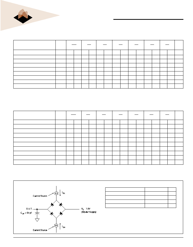
FIG. 4 AC TEST CIRCUIT
Notes:
V
Z
is programmable from -2V to +7V.
I
OL
& I
OH
programmable from 0 to 16mA.
Tester Impedance Z
0
= 75 �.
V
Z
is typically the midpoint of V
OH
and V
OL
.
I
OL
& I
OH
are adjusted to simulate a typical resistive load circuit.
ATE tester includes jig capacitance.
AC C
HARACTERISTICS
(V
CC
= 5.0V, V
SS
= 0V, T
A
= -55�C
TO
+125�C)
AC T
EST
C
ONDITIONS
Parameter
Typ
Unit
Input Pulse Levels
V
IL
= 0, V
IH
= 3.0
V
Input Rise and Fall
5
ns
Input and Output Reference Level
1.5
V
Output Timing Reference Level
1.5
V
Parameter
Symbol
-15*
-17
-20
-25
-35
-45
-55
Units
Write Cycle
Min Max Min Max
Min Max
Min Max Min
Max
Min
Max Min Max
Write Cycle Time
t
WC
1
5
1
7
20
25
35
45
55
n s
Chip Select to End of Write
t
CW
1
3
1
5
1
5
1
7
25
35
50
n s
Address Valid to End of Write
t
AW
1
3
1
5
1
5
1
7
25
35
50
n s
Data Valid to End of Write
t
DW
1
0
1
1
1
2
1
3
20
25
25
n s
Write Pulse Width
t
WP
1
3
1
5
1
5
1
7
25
35
40
n s
Address Setup Time
t
A S
2
2
2
2
2
2
2
n s
Address Hold Time
t
A H
0
0
0
0
0
5
5
n s
Output Active from End of Write t
OW
1
2
2
3
4
4
5
5
n s
Write Enable to Output in High Z
t
WHZ
1
8
9
1
1
1
3
1
5
20
20
n s
Data Hold Time
t
DH
0
0
0
0
0
0
0
n s
Parameter
Symbol
-15*
-17
-20
-25
-35
-45
-55
Units
Read Cycle
Min Max Min Max
Min Max
Min Max
Min
Max Min Max
Min Max
Read Cycle Time
tRC
15
17
20
25
35
45
55
n s
Address Access Time
tAA
15
17
20
25
35
45
55
n s
Output Hold from Address Change tOH
0
0
0
0
0
0
0
n s
Chip Select Access Time
tACS
15
17
20
25
35
45
55
n s
Output Enable to Output Valid
tOE
8
9
10
12
25
25
25
n s
Chip Select to Output in Low Z
tCLZ
1
2
2
2
2
4
4
4
n s
Output Enable to Output in Low Z tOLZ
1
0
0
0
0
0
0
0
n s
Chip Disable to Output in High Z tCHZ
1
1
2
1
2
1
2
1
2
1
5
20
20
n s
Output Disable to Output in High Z tOHZ
1
1
2
1
2
1
2
1
2
1
5
20
20
n s
*15ns Access Time available only in Commercial and Industrial Temperature. This speed is not fully characterized and is subject to change
without notice.
1. This parameter is guaranteed by design but not tested.
*15ns Access Time available only in Commercial and Industrial Temperature. This speed is not fully characterized and is subject to change
without notice.
1. This parameter is guaranteed by design but not tested.
2. The Address Setup Time of minimum 2ns is for the G2U, G1U and H1 packages. t
AS
minimum for the G4T package is 0ns.
5
White Electronic Designs Corporation (602) 437-1520 www.whiteedc.com
WS512K32-XXX
White Electronic Designs
WS32K32-XHX
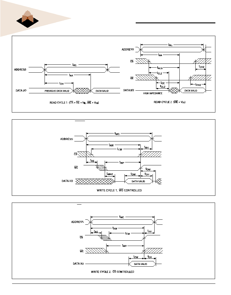
FIG. 5 TIMING WAVEFORM - READ CYCLE
FIG. 7 WRITE CYCLE - CS CONTROLLED
FIG. 6 WRITE CYCLE - WE CONTROLLED