WSE128K16-XXX
1
White Electronic Designs Corporation ∑ (602) 437-1520 ∑ www.wedc.com
White Electronic Designs
PRELIMINARY*
White Electronic Designs Corp. reserves the right to change products or specifi cations without notice.
March 2005
Rev. 3
128Kx16 SRAM/EEPROM MODULE
FEATURES
Access Times of 35ns (SRAM) and 150ns (EEPROM)
Access Times of 45ns (SRAM) and 120ns (EEPROM)
Access Times of 70ns (SRAM) and 300ns (EEPROM)
Packaging
∑ 66 pin, PGA Type, 1.075" square HIP, Hermetic
Ceramic HIP (H1) (Package 400)
∑ 68 lead, Hermetic CQFP (G2T), 22mm (0.880")
square (Package 509). Designed to fi t JEDEC 68
lead 0.990" CQFJ footprint (FIGURE 2)
128Kx16
SRAM
128Kx16
EEPROM
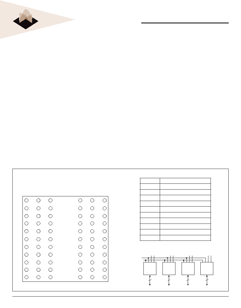
Organized as 128Kx16 of SRAM and 128Kx16 of
EEPROM Memory with separate Data Buses
Both blocks of memory are User Confi gurable as
256Kx8
Low
Power
CMOS
BLOCK DIAGRAM
PIN DESCRIPTION
ED
0-15
EEPROM Data Inputs/Outputs
SD
0-15
SRAM Data Inputs/Outputs
A
0-16
Address Inputs
SWE#
1-2
SRAM Write Enable
SCS#
1-2
SRAM Chip Selects
OE#
Output Enable
V
CC
Power Supply
GND
Ground
NC
Not Connected
EWE#
1-2
EEPROM Write Enable
ECS#
1-2
EEPROM Chip Select
Top View
FIGURE 1 ≠ WSE128K16-XH1X PIN
CONFIGURATION
Commercial, Industrial and Military Temperature
Ranges
TTL Compatible Inputs and Outputs
Built-in Decoupling Caps and Multiple Ground Pins
for Low Noise Operation
Weight - 13 grams typical
EEPROM MEMORY FEATURES
Write Endurance 10,000 Cycles
Data Retention at 25įC, 10 Years
Low
Power
CMOS
Operation
Automatic
Page
Write
Operation
Page Write Cycle Time 10ms Max.
Data Polling for End of Write Detection
Hardware and Software Data Protection
TTL Compatible Inputs and Outputs
* This product is under development, is not qualifi ed or characterized and is subject to
change without notice.
SD
8
SD
9
SD
10
A
13
A
14
A
15
A
16
NC
SD
0
SD
1
SD
2
11
22
33
44
55
66
1
12
23
34
45
56
ED
8
ED
9
ED
10
A
6
A
7
NC
A
8
A
9
ED
0
ED
1
ED
2
SD
15
SD
14
SD
13
SD
12
OE#
NC
SWE#
1
SD
7
SD
6
SD
5
SD
4
SWE
2
#
SCS
2
#
GND
SD
11
A
10
A
11
A
12
V
CC
SCS
1
#
NC
SD
3
ED
15
ED
14
ED
13
ED
12
A
0
A
1
A
2
ED
7
ED
6
ED
5
ED
5
V
CC
ECS
2
#
EWE
2
#
ED
11
A
3
A
4
A
5
EWE
1
#
ECS
1
#
GND
ED
3
EWE
1
# ECS
1
#
EWE
2
# ECS
2
#
SWE
2
# SCS
2
#
128K x 8
SRAM
8
SD
0 - 7
128K x 8
SRAM
8
SD
8 - 1 5
128K x 8
EEPROM
8
ED
0 - 7
128K x 8
EEPROM
8
ED
8 - 1 5
A
0 - 1 6
OE#
SWE
1
# SCS
1
#
WSE128K16-XXX
2
White Electronic Designs Corporation ∑ (602) 437-1520 ∑ www.wedc.com
White Electronic Designs
PRELIMINARY
White Electronic Designs Corp. reserves the right to change products or specifi cations without notice.
March 2005
Rev. 3
Top View
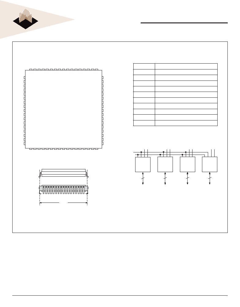
FIGURE 2 WSE128K16-XG2TX PIN CONFIGURATION
BLOCK DIAGRAM
PIN DESCRIPTION
ED
0-15
EEPROM Data Inputs/Outputs
SD
0-15
SRAM Data Inputs/Outputs
A
0-16
Address Inputs
SWE#
1-2
SRAM Write Enable
SCS#
1-2
SRAM Chip Selects
OE#
Output Enable
V
CC
Power Supply
GND
Ground
NC Not
Connected
EWE#
1-2
EEPROM Write Enable
ECS#
1-2
EEPROM Chip Select
The WEDC 68 lead G2T CQFP fi lls the same fi t and
function as the JEDEC 68 lead CQFJ or 68 PLCC. But
the G2T has the TCE and lead inspection advantage
of the CQFP form.
EWE
1
# ECS
1
#
EWE
2
# ECS
2
#
SWE
2
# SCS
2
#
128K x 8
SRAM
8
SD
0 - 7
128K x 8
SRAM
8
SD
8 - 1 5
128K x 8
EEPROM
8
ED
0 - 7
128K x 8
EEPROM
8
ED
8 - 1 5
A
0 - 1 6
OE#
SWE
1
# SCS
1
#
10
11
12
13
14
15
16
17
18
19
20
21
22
23
24
25
26
60
59
58
57
56
55
54
53
52
51
50
49
48
47
46
45
44
9 8 7 6 5 4 3 2 1 68 67 66 65 64 63 62 61
27 28 29 30 31 32 33 34 35 36 37 38 39 40 41 42 43
SD
0
SD
1
SD
2
SD
3
SD
4
SD
5
SD
6
SD
7
GND
SD
8
SD
9
SD
10
SD
11
SD
12
SD
13
SD
14
SD
15
V
CC
A
11
A
12
A
13
A
14
A
15
A
16
SCS
1
#
OE#
SCS
2
#
NC
SWE
2
#
EWE
1
#
EWE
2
#
NC
NC
NC
ED
0
ED
1
ED
2
ED
3
ED
4
ED
5
ED
6
ED
7
GND
ED
8
ED
9
ED
10
ED
11
ED
12
ED
13
ED
14
ED
15
NC
A
0
A
1
A
2
A
3
A
4
A
5
ECS
1
#
GND
ECS
2
#
SWE
1
#
A
6
A
7
A
8
A
9
A
10
V
CC
0.940"
WSE128K16-XXX
3
White Electronic Designs Corporation ∑ (602) 437-1520 ∑ www.wedc.com
White Electronic Designs
PRELIMINARY
White Electronic Designs Corp. reserves the right to change products or specifi cations without notice.
March 2005
Rev. 3
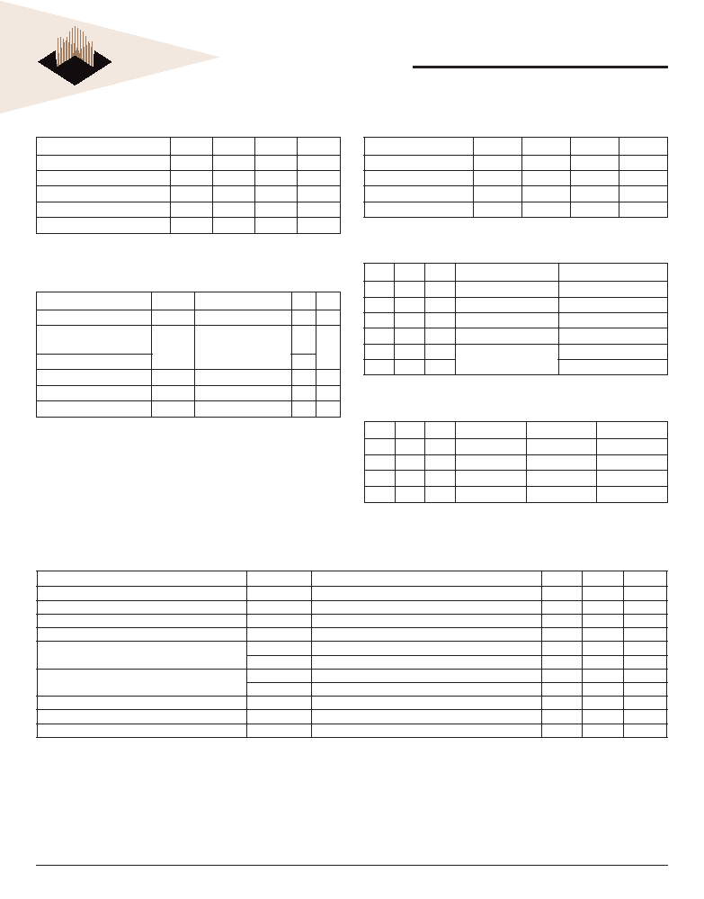
RECOMMENDED OPERATING CONDITIONS
Parameter
Symbol
Min
Max
Unit
Supply Voltage
V
CC
4.5
5.5
V
Input High Voltage
V
IH
2.0
V
CC
+ 0.3
V
Input Low Voltage
V
IL
-0.3
+0.8
V
Operating Temp. (Mil.)
T
A
-55
+125
įC
EEPROM TRUTH TABLE
CS#
OE#
WE#
Mode
Data I/O
H
X
X
Standby
High Z
L
L
H
Read
Data Out
L
H
L
Write
Data In
X
H
X
Out Disable
High Z/Data Out
X
X
H
Write
Inhibit
X
L
X
SRAM TRUTH TABLE
SCS# OE# SWE#
Mode
Data I/O
Power
H
X
X
Standby
High Z
Standby
L
L
H
Read
Data Out
Active
L
H
H
Read
High Z
Active
L
X
L
Write
Data In
Active
DC CHARACTERISTICS
V
CC
= 5.0V, GND = 0V, -55įC T
A
+125įC
Parameter
Symbol
Conditions
Min
Max
Unit
Input Leakage Current
I
LI
V
CC
= 5.5, V
IN
= GND to V
CC
10
ĶA
Output Leakage Current
I
LO
SCS# = V
IH
, OE# = V
IH
, V
OUT
= GND to V
CC
10
ĶA
SRAM Operating Supply Current x 16 Mode
I
CC
x16
SCS# = V
IL
, OE# = ECS# = V
IH
, f = 5MHz, V
CC
= 5.5
360
mA
Standby Current
ISB
ECS# = SCS# = V
IH
, OE# = V
IH
, f = 5MHz, V
CC
= 5.5
31.2
mA
SRAM Output Low Voltage
(35 to 45ns)
V
OL
I
OL
= 8.0mA, V
CC
= 4.5
0.4
V
(70ns)
V
OL
I
OL
= 2.1mA, V
CC
= 4.5
0.4
V
SRAM Output High Voltage
(35 to 45ns)
V
OH
I
OH
= -4.0mA, V
CC
= 4.5
2.4
V
(70ns)
V
OH
I
OH
= -1mA, V
CC
= 4.5
2.4
V
EEPROM Operating Supply Current x 16 Mode
I
CC1
ECS# = V
IL
, OE# = SCS# = V
IH
155
mA
EEPROM Output Low Voltage
V
OL
I
OL
= 2.1 mA, V
CC
= 4.5V
0.45
V
EEPROM Output High Voltage
V
OH1
I
OH
= 400 ĶA, V
CC
= 4.5V
2.4
V
NOTES:
1. The
I
CC
current listed includes both the DC operating current and the frequency dependent component (@ 5 MHz).
The frequency component typically is less than 2 mA/MHz, with OE at V
IH
.
2. DC test conditions: V
IL
= 0.3V, V
IH
= V
CC
- 0.3V
ABSOLUTE MAXIMUM RATINGS
Parameter
Symbol
Min
Max
Unit
Operating Temperature
T
A
-55
+125
įC
Storage Temperature
T
STG
-65
+150
įC
Signal Voltage Relative to GND
V
G
-0.5
V
CC
+0.5
V
Junction Temperature
T
J
150
įC
Supply Voltage
V
CC
-0.5
7.0
V
CAPACITANCE
T
A
= +25įC
Parameter
Symbol Conditions Max Unit
OE# capacitance
C
OE
V
IN
= 0 V, f = 1.0 MHz
50
pF
WE#
1-4
capacitance
HIP (PGA)
C
WE
V
IN
= 0 V, f = 1.0 MHz
20
pF
CQFP G2T
20
CS#
1-4
capacitance
C
CS
V
IN
= 0 V, f = 1.0 MHz
20
pF
Data I/O capacitance
C
I/O
V
I/O
= 0 V, f = 1.0 MHz
20
pF
Address input capacitance
C
AD
V
IN
= 0 V, f = 1.0 MHz
50
pF
This parameter is guaranteed by design but not tested.
WSE128K16-XXX
4
White Electronic Designs Corporation ∑ (602) 437-1520 ∑ www.wedc.com
White Electronic Designs
PRELIMINARY
White Electronic Designs Corp. reserves the right to change products or specifi cations without notice.
March 2005
Rev. 3
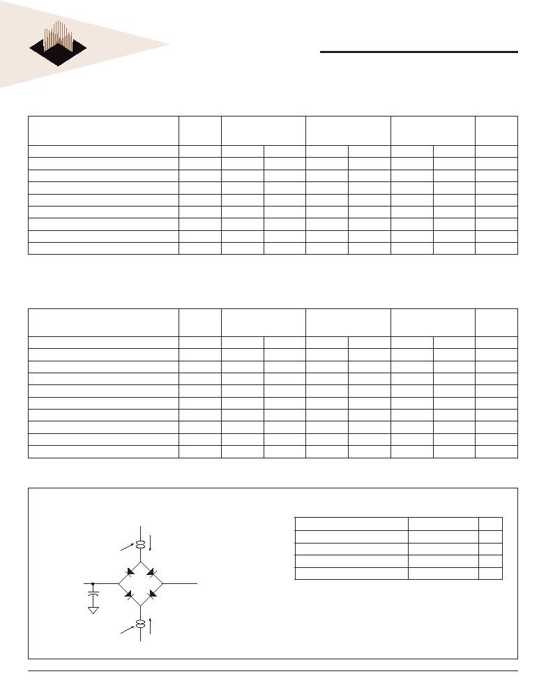
FIGURE 3 ≠ AC TEST CIRCUIT
AC TEST CONDITIONS
Parameter
Typ
Unit
Input Pulse Levels
V
IL
= 0, V
IH
= 3.0
V
Input Rise and Fall
5
ns
Input and Output Reference Level
1.5
V
Output Timing Reference Level
1.5
V
NOTES:
V
Z
is programmable from -2V to +7V.
I
OL
& I
OH
programmable from 0 to 16mA.
Tester Impedance Z0 = 75 .
V
Z
is typically the midpoint of V
OH
and V
OL
.
I
OL
& I
OH
are adjusted to simulate a typical resistive load circuit.
ATE tester includes jig capacitance.
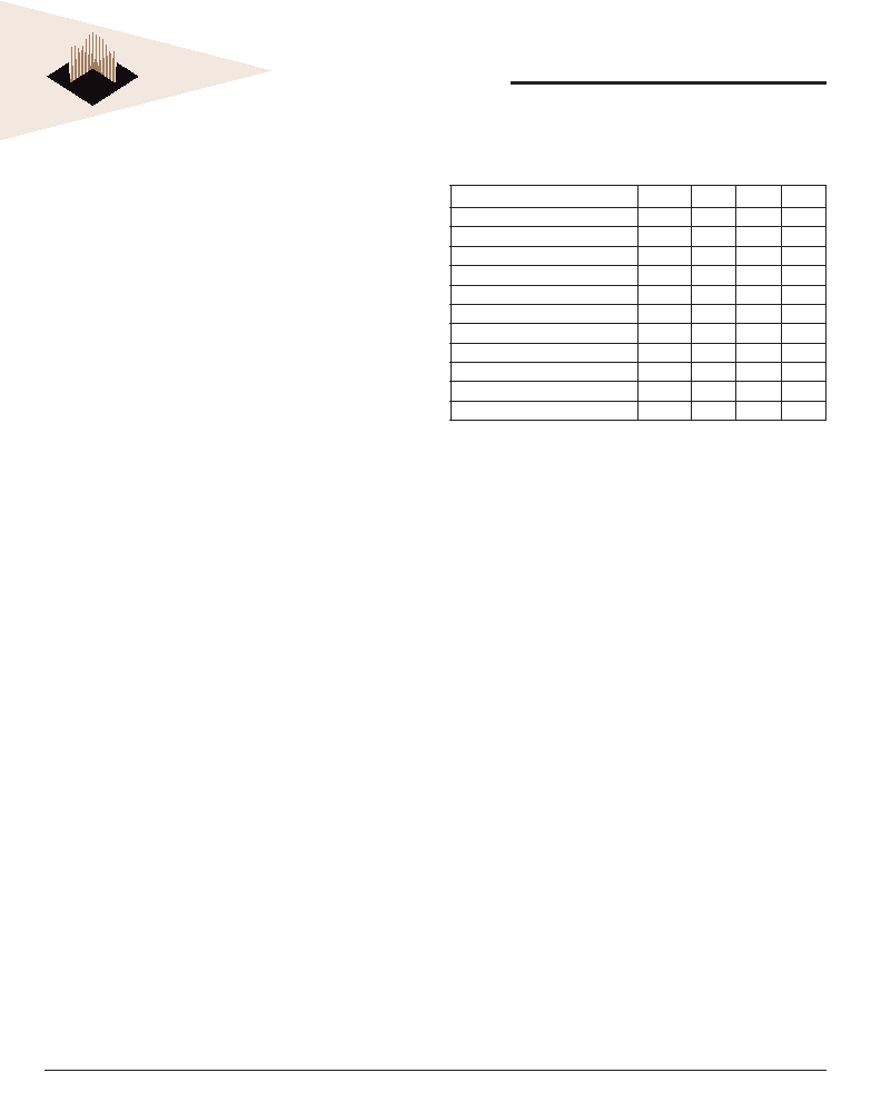
SRAM AC CHARACTERISTICS
V
CC
= 5.0V, GND = 0V, -55įC T
A
+125įC
Parameter
Read Cycle
Symbol
-35
-45
-70
Units
Min
Max
Min
Max
Min
Max
Read Cycle Time
t
RC
35
45
70
ns
Address Access Time
t
AA
35
45
70
ns
Output Hold from Address Change
t
OH
0
0
5
ns
Chip Select Access Time
t
ACS
35
45
70
ns
Output Enable to Output Valid
t
OE
20
25
35
ns
Chip Select to Output in Low Z
t
CLZ1
3
3
5
ns
Output Enable to Output in Low Z
t
OLZ1
0
0
5
ns
Chip Disable to Output in High Z
t
CHZ1
20
20
25
ns
Output Disable to Output in High Z
t
OHZ1
20
20
25
ns
1. This parameter is guaranteed by design but not tested.
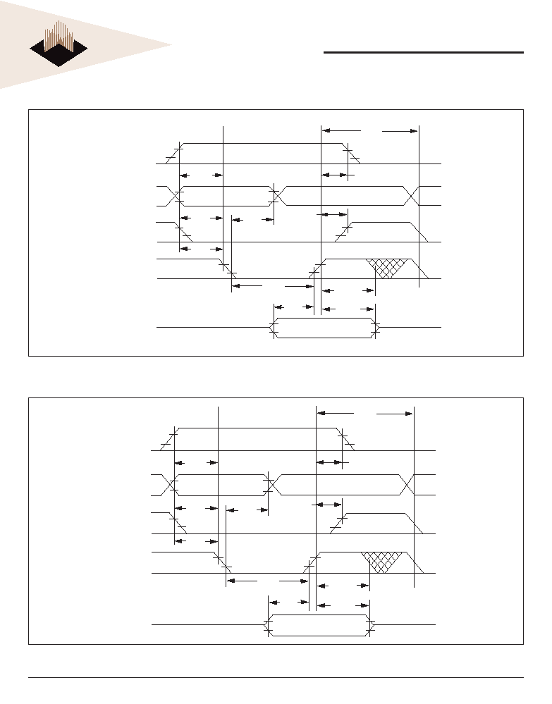
SRAM AC CHARACTERISTICS
V
CC
= 5.0V, GND = 0V, -55įC T
A
+125įC
Parameter
Write Cycle
Symbol
-35
-45
-70
Units
Min
Max
Min
Max
Min
Max
Write Cycle Time
t
WC
35
45
70
ns
Chip Select to End of Write
t
CW
25
30
60
ns
Address Valid to End of Write
t
AW
25
30
60
ns
Data Valid to End of Write
t
DW
20
25
30
ns
Write Pulse Width
t
WP
25
30
50
ns
Address Setup Time
t
AS
0
0
5
ns
Address Hold Time
t
AH
0
0
5
ns
Output Active from End of Write
t
OW1
4
4
5
ns
Write Enable to Output in High Z
t
WHZ1
20
25
25
ns
Data Hold Time
t
DH
0
0
0
ns
1. This parameter is guaranteed by design but not tested.
I
Current Source
D.U.T.
C = 50 pf
eff
I
OL
V 1.5V
(Bipolar Supply)
Z
Current Source
OH

WSE128K16-XXX
5
White Electronic Designs Corporation ∑ (602) 437-1520 ∑ www.wedc.com
White Electronic Designs
PRELIMINARY
White Electronic Designs Corp. reserves the right to change products or specifi cations without notice.
March 2005
Rev. 3
FIGURE 4 ≠ SRAM READ CYCLES
ADDRESS
SRAM
DATA I/O
PREVIOUS DATA VALID
DATA VALID
t
RC
t
AA
READ CYCLE 1, (SCS# = OE# = V
IL
, SWE# = V
IH
)
t
OH
ADDRESS
SCS#
SOE#
SRAM
DATA I/O
t
RC
t
AA
t
ACS
t
CLZ
t
OE
t
OLZ
t
CHZ
t
OHZ
HIGH IMPEDANCE
READ CYCEL 2, (SWE# = V
IH
)
DATA VALID
FIGURE 5 ≠ SRAM WRITE CYCLE SWE# CONTROLLED
ADDRESS
SCS#
SWE#
SRAM
DATA I/O
t
WC
t
AW
t
CW
t
AH
t
WP
t
OW
t
AS
t
WHZ
t
DW
t
DH
DATA VALID
WRITE CYCLE 1, SWE# CONTROLLED
FIGURE 6 ≠ SRAM WRITE CYCEL SCS# CONTROLLED
ADDRESS
SCS#
SWE#
SRAM
DATA I/O
t
WC
t
AW
t
CW
t
AS
t
AH
t
DH
t
DW
t
WP
DATA VALID
WRITE CYCLE 2, SCS# CONTROLLED
WSE128K16-XXX
6
White Electronic Designs Corporation ∑ (602) 437-1520 ∑ www.wedc.com
White Electronic Designs
PRELIMINARY
White Electronic Designs Corp. reserves the right to change products or specifi cations without notice.
March 2005
Rev. 3
EEPROM WRITE
A write cycle is initiated when OE# is high and a low pulse
is on EWE# or ECS# with ECS# or EWE# low. The address
is latched on the falling edge of ECS# or EWE# whichever
occurs last. The data is latched by the rising edge of ECS#
or EWE#, whichever occurs fi rst. A byte write operation
will automatically continue to completion.
WRITE CYCLE TIMING
Figures 7 and 8 show the write cycle timing relationships.
A write cycle begins with address application, write enable
and chip select. Chip select is accomplished by placing the
ECS# line low. Write enable consists of setting the EWE#
line low. The write cycle begins when the last of either
ECS# or EWE# goes low.
The EWE# line transition from high to low also initiates
an internal 150 Ķsec delay timer to permit page mode
operation. Each subsequent EWE# transition from high
to low that occurs before the completion of the 150 Ķsec
time out will restart the timer from zero. The operation of
the timer is the same as a retriggerable one-shot.
EEPROM AC WRITE CHARACTERISTICS
V
CC
= 5.0V, GND = 0V, -55įC T
A
+125įC
Write Cycle Parameter
Symbol
Min
Max
Unit
Write Cycle Time, TYP = 6ms
t
WC
10
ms
Address Set-up Time
t
AS
0
ns
Write Pulse Width (EWE# or ECS#)
t
WP
150
ns
Chip Select Set-up Time
t
CS
0
ns
Address Hold Time
t
AH
100
ns
Data Hold Time
t
DH
10
ns
Chip Select Hold Time
t
CSH
0
ns
Data Set-up Time
t
DS
100
ns
Output Enable Set-up Time
t
OES
10
ns
Output Enable Hold Time
t
OEH
10
ns
Write Pulse Width High
t
WPH
50
ns
WSE128K16-XXX
7
White Electronic Designs Corporation ∑ (602) 437-1520 ∑ www.wedc.com
White Electronic Designs
PRELIMINARY
White Electronic Designs Corp. reserves the right to change products or specifi cations without notice.
March 2005
Rev. 3
FIGURE 7 ≠ EEPROM WRITE WAVEFORMS EWE# CONTROLLED
FIGURE 8 ≠ EEPROM WRITE WAVEFORMS ECS# CONTROLLED
t
DH
t
WPH
t
WP
t
CSH
t
OEH
t
AH
t
OES
t
AS
t
CS
OE#
ADDRESS
ECS#
1-2
EWE#
1-2
EEPROM
DATA IN
t
WC
t
DS
t
DH
t
WPH
t
WP
t
CSH
t
OEH
t
AH
t
OES
t
AS
t
CS
OE#
ADDRESS
ECS#
1-2
EWE#
1-2
EEPROM
DATA IN
t
DS
t
WC

WSE128K16-XXX
8
White Electronic Designs Corporation ∑ (602) 437-1520 ∑ www.wedc.com
White Electronic Designs
PRELIMINARY
White Electronic Designs Corp. reserves the right to change products or specifi cations without notice.
March 2005
Rev. 3
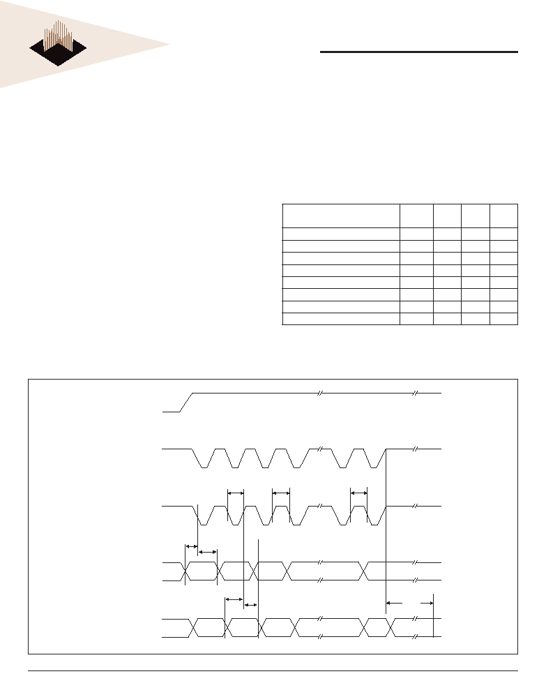
FIGURE 9 ≠ EEPROM READ WAVEFORMS
EEPROM READ
The WSE128K16-XXX EEPROM stores data at the
memory location determined by the address pins. When
ECS# and OE# are low and EWE# is high, this data is
present on the outputs. When ECS# and OE# are high,
the outputs are in a high impedance state. This two line
control prevents bus contention.
Note: OE# may be delayed up to t
ACS
- t
OE
after the falling edge of ECS# without impact on t
OE
or by t
ACC
- t
OE
after an address change without impact on t
ACC
.
EEPROM AC READ CHARACTERISTICS
V
CC
= 5.0V, GND = 0V, -55įC T
A
+125įC
Read Cycle Parameter
Symbol
-120
-150
-300
Unit
Min
Max
Min
Max
Min
Max
Read Cycle Time
t
RC
120
150
300
ns
Address Access Time
t
ACC
120
150
300
ns
Chip Select Access Time
t
ACS
120
150
300
ns
Output Hold from Add. Change, OE# or ECS#
t
OH
0
0
0
ns
Output Enable to Output Valid
t
OE
0
50
0
55
0
85
ns
Chip Select or OE# to High Z Output
t
DF
70
70
70
ns
t
OH
ADDRESS
ECS#
1-2
OE#
EEPROM
DATA
OUTPUT
t
DF
t
ACC
t
RC
t
OE
t
ACS
OUTPUT
VALID
ADDRESS VALID
HIGH Z

WSE128K16-XXX
9
White Electronic Designs Corporation ∑ (602) 437-1520 ∑ www.wedc.com
White Electronic Designs
PRELIMINARY
White Electronic Designs Corp. reserves the right to change products or specifi cations without notice.
March 2005
Rev. 3
EEPROM DATA POLLING
The WSE128K16-XXX offers a data polling feature for
the EEPROM which allows a faster method of writing to
the device. Figure 11 shows the timing diagram for this
function. During a byte or page write cycle, an attempted
read of the last byte written will result in the complement
of the written data on D7 (for each chip.) Once the write
cycle has been completed, true data is valid on all outputs
and the next cycle may begin. Data polling may begin at
any time during the write cycle.
FIGURE 10 ≠ EEPROM DATA POLLING WAVEFORMS
EEPROM DATA POLLING CHARACTERISTICS
V
CC
= 5.0V, GND = 0V, -55įC T
A
+125įC
Parameter
Symbol
Min
Max
Unit
Data Hold Time
t
DH
10
ns
OE# Hold Time
t
OEH
10
ns
OE# To Output Valid
t
OE
55
ns
Write Recovery Time
t
WR
0
ns
EWE#
1-2
ECS#
1-2
OE#
ED
7
ADDRESS
t
OEH
t
DH
t
OE
t
WR
HIGH Z
WSE128K16-XXX
10
White Electronic Designs Corporation ∑ (602) 437-1520 ∑ www.wedc.com
White Electronic Designs
PRELIMINARY
White Electronic Designs Corp. reserves the right to change products or specifi cations without notice.
March 2005
Rev. 3
EEPROM PAGE WRITE OPERATION
The WSE128K16-XXX has a page write operation
that allows one to 128 bytes of data to be written into
the device and consecutively loads during the internal
programming period. Successive bytes may be loaded
in the same manner after the fi rst data byte has been
loaded. An internal timer begins a time out operation at
each write cycle. If another write cycle is completed within
150Ķs or less, a new time out period begins. Each write
cycle restarts the delay period. The write cycles can be
continued as long as the interval is less than the time out
period.
The usual procedure is to increment the least signifi cant
address lines from A0 through A6 at each write cycle. In
this manner a page of up to 128 bytes can be loaded in
to the EEPROM in a burst mode before beginning the
relatively long interval programming cycle.
FIGURE 11 ≠ EEPROM PAGE MODE WRITE WAVEFORMS
EEPROM PAGE WRITE CHARACTERISTICS
V
CC
= 5.0V, GND = 0V, -55įC T
A
+125įC
Page Mode Write Characteristics
Parameter
Symbol
Min
Max
Unit
Write Cycle Time, TYP = 6ms
t
WC
10
ms
Address Set-up Time
t
AS
0
ns
Address Hold Time (1)
t
AH
100
ns
Data Set-up Time
t
DS
100
ns
Data Hold Time
t
DH
10
ns
Write Pulse Width
t
WP
150
ns
Byte Load Cycle Time
t
BLC
150
Ķs
Write Pulse Width High
t
WPH
50
ns
NOTE:
1. Page address must remain valid for duration of write cycle.
BYTE 0
BYTE 1
BYTE 2
BYTE 3
VALID
DATA
VALID
ADDRESS
t
WC
t
BLC
t
WPH
t
WP
BYTE 127
t
DS
t
DH
t
AS
t
AH
OE#
ECS#
1-2
EWE#
1-2
ADDRESS
EEPROM
DATA
After the 150Ķs time out is completed, the EEPROM
begins an internal write cycle. During this cycle the entire
page of bytes will be written at the same time. The internal
programming cycle is the same regardless of the number
of bytes accessed.

WSE128K16-XXX
11
White Electronic Designs Corporation ∑ (602) 437-1520 ∑ www.wedc.com
White Electronic Designs
PRELIMINARY
White Electronic Designs Corp. reserves the right to change products or specifi cations without notice.
March 2005
Rev. 3
LOAD DATA AA
TO
ADDRESS 5555
LOAD DATA 55
TO
ADDRESS 2AAA
LOAD DATA A0
TO
ADDRESS 5555
LOAD DATA XX
TO
ANY ADDRESS
(4)
LOAD LAST BYTE
TO
LAST ADDRESS
FIGURE 12 ≠ EEPROM SOFTWARE DATA PROTECTION ENABLE ALGORITHM
(1)
WRITES ENABLED
(2)
NOTES:
1. Data Format: ED7 - ED0 (Hex);
Address Format: A16 - A0 (Hex).
2. Write Protect state will be activated at end of write even if no other data is loaded.
3. Write Protect state will be deactivated at end of write period even if no other data is loaded.
4. 1 to 128 bytes of data may be loaded.
ENTER DATA
PROTECT STATE

WSE128K16-XXX
12
White Electronic Designs Corporation ∑ (602) 437-1520 ∑ www.wedc.com
White Electronic Designs
PRELIMINARY
White Electronic Designs Corp. reserves the right to change products or specifi cations without notice.
March 2005
Rev. 3
EEPROM HARDWARE DATA
PROTECTION
These features protect against inadvertent writes to
the WSE128K16-XXX. These are included to improve
reliability during normal operation:
a) V
CC
power on delay
As V
CC
climbs past 3.8V typical the device will wait
5 msec typical before allowing write cycles.
b) V
CC
sense
While below 3.8V typical write cycles are inhibited.
c) Write
inhibiting
Holding OE# low and either ECS# or EWE# high
inhibits write cycles.
d) Noise
fi
lter
Pulses of <8ns (typ) on EWE# or ECS# will not
initiate a write cycle.
EEPROM SOFTWARE DATA
PROTECTION
A software write protection feature may be enabled
or disabled by the user. When shipped by WEDC, the
WSE128K16-XXX has the feature disabled. Write access
to the device is unrestricted.
To enable software write protection, the user writes three
access code bytes to three special internal locations.
Once write protection has been enabled, each write to the
EEPROM must use the same three byte write sequence
to permit writing. After setting software data protection,
any attempt to write to the device without the three-byte
command sequence will start the internal write timers. No
data will be written to the device, however, for the duration
of twc. The write protection feature can be disabled by
a six byte write sequence of specifi c data to specifi c
locations. Power transitions will not reset the software
write protection.
Each 128K byte block of the EEPROM has independent
write protection. One or more blocks may be enabled and
the rest disabled in any combination. The software write
protection guards against inadvertent writes during power
transitions, or unauthorized modifi cation using a PROM
programmer.
FIGURE 13 ≠ EEPROM SOFTWARE DATA
PROTECTION DISABLE ALGORITHM
(1)
EXIT DATA
(3)
PROTECT STATE
NOTES:
1. Data Format: ED7 - ED0 (Hex);
Address Format: A16 - A0 (Hex).
2. Write Protect state will be activated at end of write even if no other data
is loaded.
3. Write Protect state will be deactivated at end of write period even if no
other data is loaded.
4. 1 to 128 bytes of data may be loaded.
LOAD DATA AA
TO
ADDRESS 5555
LOAD DATA 55
TO
ADDRESS 2AAA
LOAD DATA 80
TO
ADDRESS 5555
LOAD DATA AA
TO
ADDRESS 5555
LOAD DATA 55
TO
ADDRESS 2AAA
LOAD DATA 20
TO
ADDRESS 5555
LOAD DATA XX
TO
ANY ADDRESS
(4)
LOAD LAST BYTE
TO
LAST ADDRESS

WSE128K16-XXX
13
White Electronic Designs Corporation ∑ (602) 437-1520 ∑ www.wedc.com
White Electronic Designs
PRELIMINARY
White Electronic Designs Corp. reserves the right to change products or specifi cations without notice.
March 2005
Rev. 3
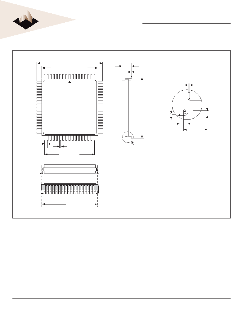
PACKAGE 400: 66 PIN, PGA TYPE, CERAMIC HEX-IN-LINE PACKAGE, HIP (H1)
ALL LINEAR DIMENSIONS ARE MILLIMETERS AND PARENTHETICALLY IN INCHES
PIN 1 IDENTIFIER
SQUARE PAD
ON BOTTOM
27.3 (1.075) Ī 0.25 (0.010) SQ
3.81 (0.150)
Ī 0.13 (0.005)
1.42 (0.056) Ī 0.13 (0.005)
0.76 (0.030) Ī 0.13 (0.005)
1.27 (0.050) Ī TYP DIA
25.4 (1.0) TYP
0.46 (0.018) Ī 0.05 (0.002) DIA
4.34 (0.171)
MAX
2.54 (0.100)
TYP
15.24 (0.600) TYP
25.4 (1.0) TYP
WSE128K16-XXX
14
White Electronic Designs Corporation ∑ (602) 437-1520 ∑ www.wedc.com
White Electronic Designs
PRELIMINARY
White Electronic Designs Corp. reserves the right to change products or specifi cations without notice.
March 2005
Rev. 3
0.38 (0.015) Ī 0.05 (0.002)
0.27 (0.011) Ī 0.04 (0.002)
25.15 (0.990) Ī 0.26 (0.010) SQ
1.27 (0.050) TYP
24.03 (0.946)
Ī 0.26 (0.010)
22.36 (0.880) Ī 0.26 (0.010) SQ
20.3 (0.800) REF
4.57 (0.180) MAX
0.19 (0.007)
Ī 0.06 (0.002)
23.87
(0.940) REF
1.0 (0.040)
Ī 0.127 (0.005)
0.25 (0.010) REF
1
į / 7į
R 0.25
(0.010)
DETAIL A
SEE DETAIL "A"
Pin 1
0.940"
TYP
PACKAGE 509: 68 LEAD, CERAMIC QUAD FLAT PACK, CQFP (G2T)
ALL LINEAR DIMENSIONS ARE MILLIMETERS AND PARENTHETICALLY IN INCHES
The WEDC 68 lead G2T CQFP fi lls the same
fi t and function as the JEDEC 68 lead CQFJ or
68 PLCC. But the G2T has the TCE and lead
inspection advantage of the CQFP form.
WSE128K16-XXX
15
White Electronic Designs Corporation ∑ (602) 437-1520 ∑ www.wedc.com
White Electronic Designs
PRELIMINARY
White Electronic Designs Corp. reserves the right to change products or specifi cations without notice.
March 2005
Rev. 3
ORDERING INFORMATION
LEAD FINISH:
Blank = Gold plated leads
A = Solder dip leads
DEVICE GRADE:
M
=
Military
Screened -55įC
to
+125įC
I = Industrial
-40įC to +85įC
C
=
Commercial
0įC
to
+70įC
PACKAGE TYPE:
H1 = 1.075" sq. Ceramic Hex-In-line Package, HIP (Package 400)
G2T = 22.4mm Ceramic Quad Flat Pack, CQFP (Package 509)
ACCESS TIME (ns)
35 = 35ns SRAM and 150ns EEPROM
42 = 45ns SRAM and 120ns EEPROM
73 = 70ns SRAM and 300ns EEPROM
ORGANIZATION, 128K x 16
EEPROM
SRAM
WHITE ELECTRONIC DESIGNS CORP.
W S E 128K16 - XXX X X X