1
White Electronic Designs Corporation ∑ (602) 437-1520 ∑ www.whiteedc.com
WSF128K16-XXX
May 2001 Rev. 5
128Kx16 SRAM/FLASH MODULE, SMD 5962-96900
FEATURES
n Access Times of 35ns (SRAM) and 70ns (FLASH)
n Access Times of 70ns (SRAM) and 120ns (FLASH)
n Packaging
∑ 66-pin, PGA Type, 1.075 inch square HIP, Hermetic
Ceramic HIP (Package 400)
∑ 66-pin, PGA Type, 1.185 inch square HIP, Hermetic
Ceramic HIP (Package 401)
∑ 68 lead, Hermetic CQFP (G1U), 22.4mm (0.880
inch) square (Package 519). Designed to fit JEDEC
68 lead 0.990" CQFJ footprint (Fig. 2)
n 128Kx16 SRAM
n 128Kx16 5V FLASH
n Organized as 128Kx16 of SRAM and 128Kx16 of Flash
Memory with separate Data Buses
n Both blocks of memory are User Configurable as
256Kx8
n Low Power CMOS
n Commercial, Industrial and Military Temperature Ranges
n TTL Compatible Inputs and Outputs
n Built-in Decoupling Caps and Multiple Ground Pins for
Low Noise Operation
n Weight
∑ WSF128K16-XHX - 13 grams typical
∑ WSF128K16-H1X - 13 grams typical
∑ WSF128K16-XG1UX - 5 grams typical
FLASH MEMORY FEATURES
n 10,000 Erase/Program Cycles
n Sector Architecture
∑ 8 equal size sectors of 16K bytes each
∑ Any combination of sectors can be concurrently
erased.
Also suppor ts full chip erase
n 5 Volt Programming; 5V ± 10% Supply
n Embedded Erase and Program Algorithms
n Hardware Write Protection
n Page Program Operation and Internal Program Control
Time.
Note: For programming information refer to Flash Programming 1M5
Application Note.
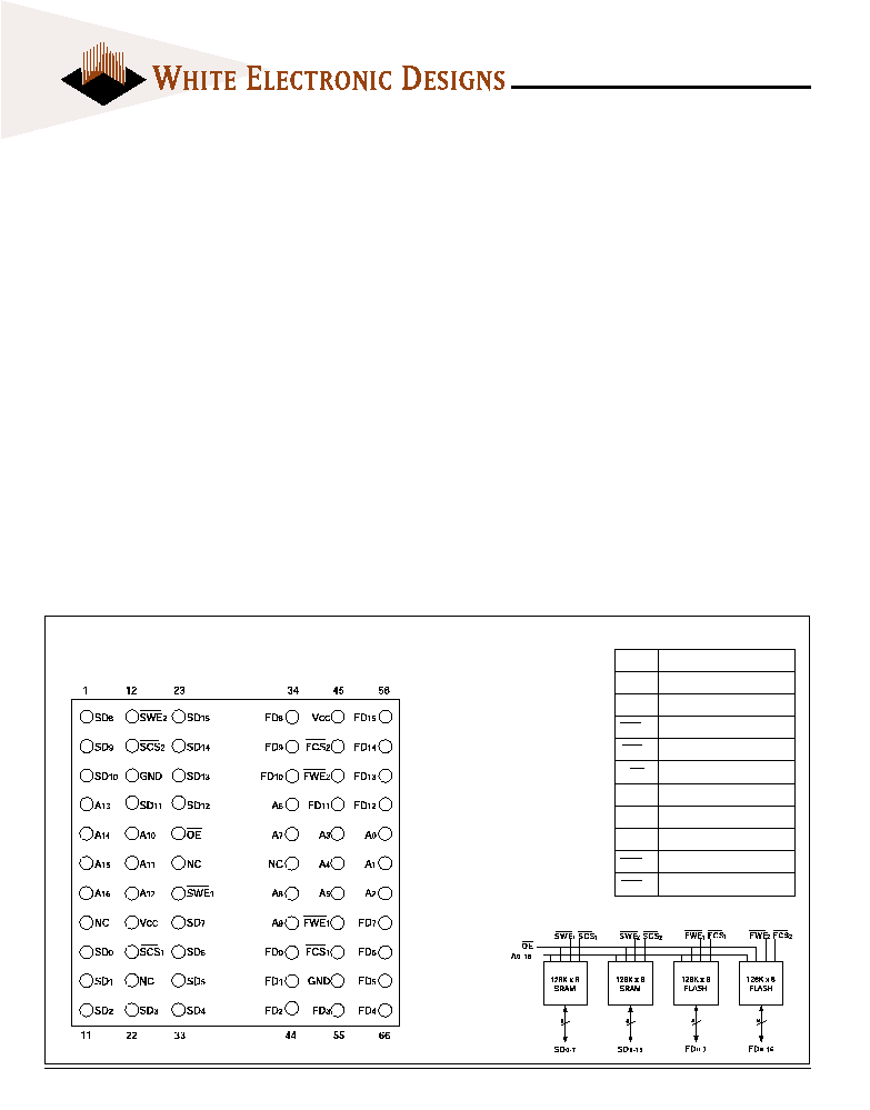
B
LOCK
D
IAGRAM
P
IN
D
ESCRIPTION
FD
0-15
Flash Data Inputs/Outputs
SD
0-15
SRAM Data Inputs/Outputs
A
0-16
Address Inputs
SWE
1-2
SRAM Write Enable
SCS
1-2
SRAM Chip Selects
OE
Output Enable
V
CC
Power Supply
GND
Ground
NC
Not Connected
FWE
1-2
Flash Write Enable
FCS
1-2
Flash Chip Select
T
OP
V
IEW
F
IG
.1
P
IN
C
ONFIGURATION
F
OR
WSF128K16-XHX A
ND
WSF128K16-XH1X

2
White Electronic Designs Corporation ∑ Phoenix AZ ∑ (602) 437-1520
WSF128K16-XXX
T
OP
V
IEW
F
IG
. 2
P
IN
C
ONFIGURATION
F
OR
WSF128K16-XG1UX
B
LOCK
D
IAGRAM
P
IN
D
ESCRIPTION
FD
0-15
Flash Data Inputs/Outputs
SD
0-15
SRAM Data Inputs/Outputs
A
0-16
Address Inputs
SWE
1-2
SRAM Write Enable
SCS
1-2
SRAM Chip Selects
OE
Output Enable
V
CC
Power Supply
GND
Ground
NC
Not Connected
FWE
1-2
Flash Write Enable
FCS
1-2
Flash Chip Select
The WEDC 68 lead G1U CQFP
fills the same fit and function
as the JEDEC 68 lead CQFJ or
68 PLCC. But the G1U has the
TCE and lead inspection
advantage of the CQFP form.
3
White Electronic Designs Corporation ∑ (602) 437-1520 ∑ www.whiteedc.com
WSF128K16-XXX
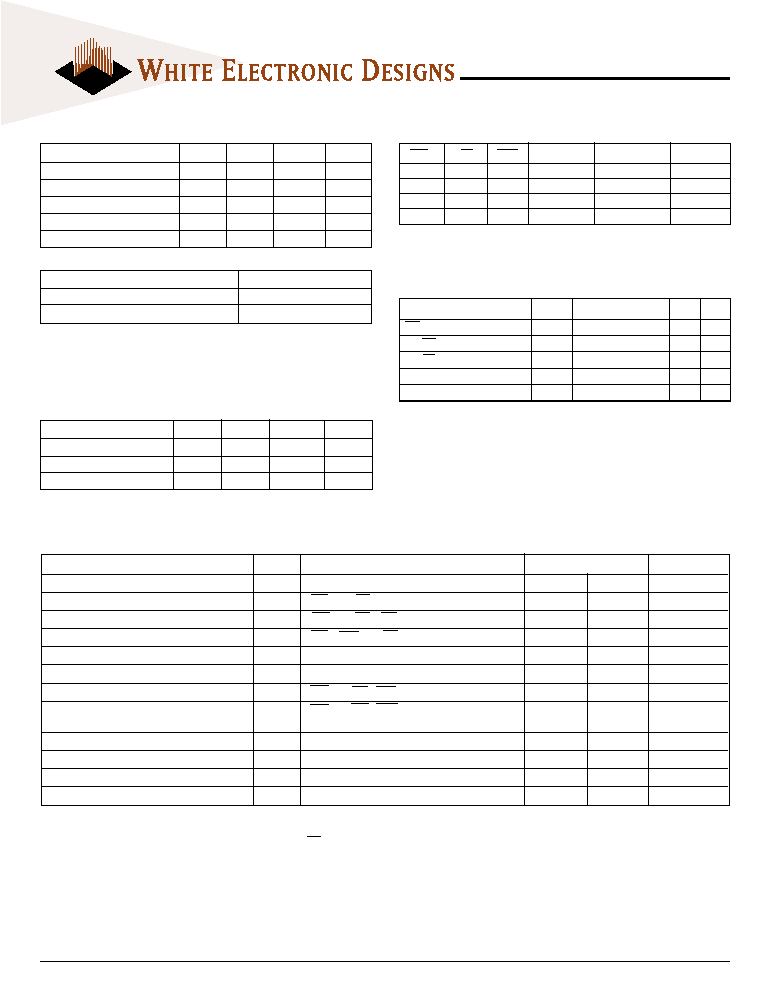
A
BSOLUTE
M
AXIMUM
R
ATINGS
DC C
HARACTERISTICS
(VCC = 5.0V, VSS = 0V, TA = -55∞C
TO
+125∞C)
Parameter
Symbol
Conditions
Min
Max
Unit
Input Leakage Current
I
L I
V
CC
= 5.5, V
IN
= GND to V
CC
10
µA
Output Leakage Current
I
L O
SCS = V
IH
, OE = V
IH,
V
OUT
= GND to V
CC
10
µA
SRAM Operating Supply Current x 16 Mode
I
CCx16
SCS = V
IL
, OE = FCS = V
IH,
f = 5MHz, V
CC
= 5.5
360
mA
Standby Current
I
SB
FCS = SCS = V
IH
, OE = V
IH,
f = 5MHz, V
CC
= 5.5
40
mA
SRAM Output Low Voltage
V
OL
I
OL
= 2.1mA, V
CC
= 4.5
0.4
V
SRAM Output High Voltage
V
OH
I
OH
= -1.0mA, V
CC
= 4.5
2.4
V
Flash V
CC
Active Current for Read (1)
I
C C 1
FCS = V
IL
, OE = SCS = V
IH
100
mA
Flash V
CC
Active Current for Program or
I
C C 2
FCS = V
IL
, OE = SCS = V
IH
130
mA
Erase (2)
Flash Output Low Voltage
V
OL
I
OL
= 8.0mA, V
CC
= 4.5
0.45
V
Flash Output High Voltage
V
OH1
I
OH
= -2.5 mA, V
CC
= 4.5
0.85 x V
CC
V
Flash Output High Voltage
V
OH2
I
OH
= -100 µA, V
CC
= 4.5
V
CC
-0.4
V
Flash Low V
CC
Lock Out Voltage
V
LKO
3.2
V
Parameter
Flash Data Retention
10 years
Flash Endurance (write/erase cycles)
10,000
NOTES:
1. Stresses above the absolute maximum rating may cause permanent damage to
the device. Extended operation at the maximum levels may degrade
performance and affect reliability.
Parameter
Symbol
Min
Max
Unit
Supply Voltage
V
CC
4.5
5.5
V
Input High Voltage
V
IH
2.2
V
CC
+ 0.3
V
Input Low Voltage
V
IL
-0.5
+0.8
V
R
ECOMMENDED
O
PERATING
C
ONDITIONS
Parameter
Symbol
Min
Max
Unit
Operating Temperature
T
A
-55
+125
∞C
Storage Temperature
T
STG
-65
+150
∞C
Signal Voltage Relative to GND
V
G
-0.5
7.0
V
Junction Temperature
T
J
150
∞C
Supply Voltage
V
CC
-0.5
7.0
V
NOTES:
1. The ICC current listed includes both the DC operating current and the frequency dependent component (@ 5 MHz).
The frequency component typically is less than 2 mA/MHz, with OE at VIH.
2. ICC active while Embedded Algorithm (program or erase) is in progress.
3. DC test conditions: VIL = 0.3V, VIH = VCC - 0.3V
SRAM T
RUTH
T
ABLE
SCS
OE
SWE
Mode
Data I/O
Power
H
X
X
Standby
High Z
Standby
L
L
H
Read
Data Out
Active
L
H
H
Read
High Z
Active
L
X
L
Write
Data In
Active
C
APACITANCE
(TA = +25∞C)
Test
Symbol
Condition
Max Unit
OE Capacitance
C
OE
V
IN
= 0V, f = 1.0MHz 50
pF
F/S WE 1-2 Capacitance
C
WE
V
IN
= 0V, f = 1.0MHz 20
pF
F/S CS 1-2 Capacitance
C
CS
V
IN
= 0V, f = 1.0MHz 20
pF
SD
0
-
15
/FD
0
-
15
Capacitance
C
I
/
O
V
IN
= 0V, f = 1.0MHz 20
pF
A
0
- A
16
Capacitance
C
AD
V
IN
= 0V, f = 1.0MHz 50
pF
This parameter is guaranteed by design but not tested.
4
White Electronic Designs Corporation ∑ Phoenix AZ ∑ (602) 437-1520
WSF128K16-XXX
Parameter
Symbol
-35
-70
Unit
Read Cycle
Min Max
Min Max
Read Cycle Time
t
RC
35
70
ns
Address Access Time
t
AA
35
70
ns
Output Hold from Address Change
t
OH
0
3
ns
Chip Select Access Time
t
ACS
35
70
ns
Output Enable to Output Valid
t
OE
20
35
ns
Chip Select to Output in Low Z
t
C L Z
1
3
3
ns
Output Enable to Output in Low Z
t
OLZ
1
0
0
ns
Chip Disable to Output in High Z
t
CHZ
1
20
25
ns
Output Disable to Output in High Z
t
OHZ
1
20
25
ns
SRAM AC C
HARACTERISTICS
(VCC = 5.0V, TA = -55∞C
TO
+125∞C)
Parameter
Symbol
-35
-70
Unit
Write Cycle
Min Max
Write Cycle Time
t
WC
35
70
ns
Chip Select to End of Write
t
CW
25
60
ns
Address Valid to End of Write
t
AW
25
60
ns
Data Valid to End of Write
t
DW
20
30
ns
Write Pulse Width
t
WP
25
50
ns
Address Setup Time
t
AS
0
5
ns
Address Hold Time
t
AH
0
5
ns
Output Active from End of Write
t
OW
1
4
5
ns
Write Enable to Output in High Z
t
WHZ
1
20
25
ns
Data Hold from Write Time
t
DH
0
0
ns
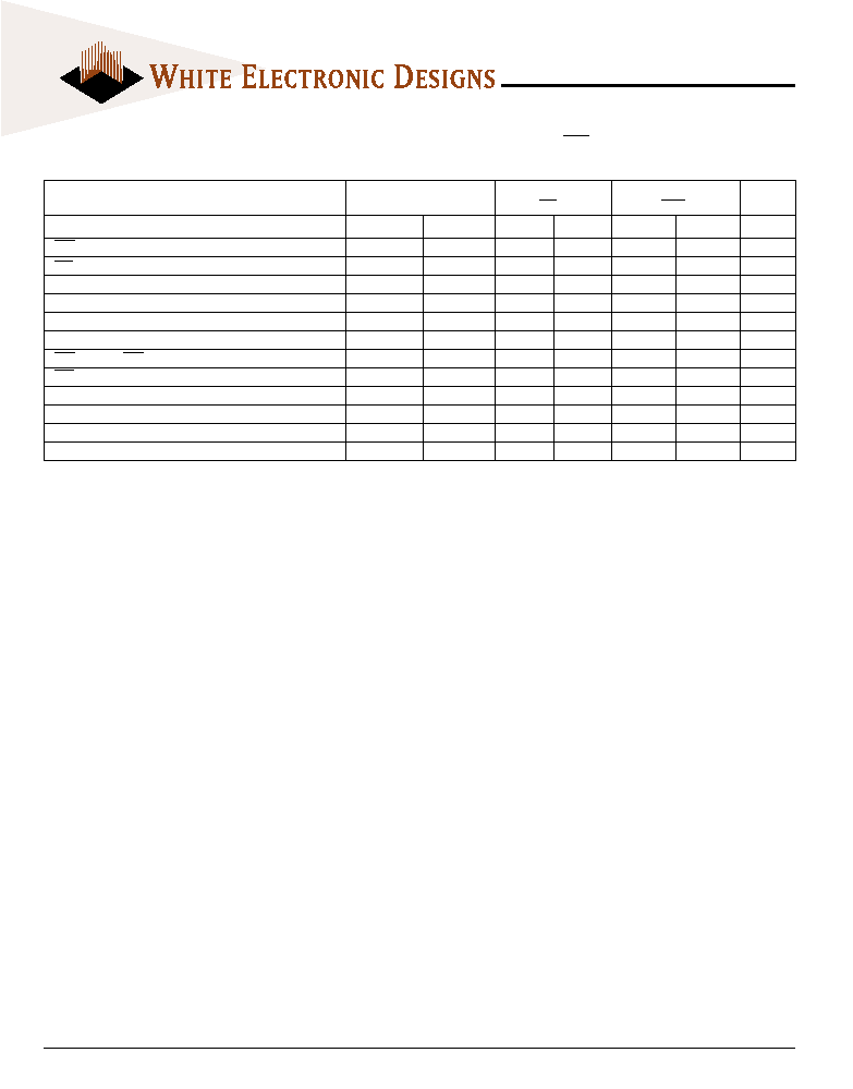
SRAM AC C
HARACTERISTICS
(VCC = 5.0V, TA = -55∞C
TO
+125∞C)
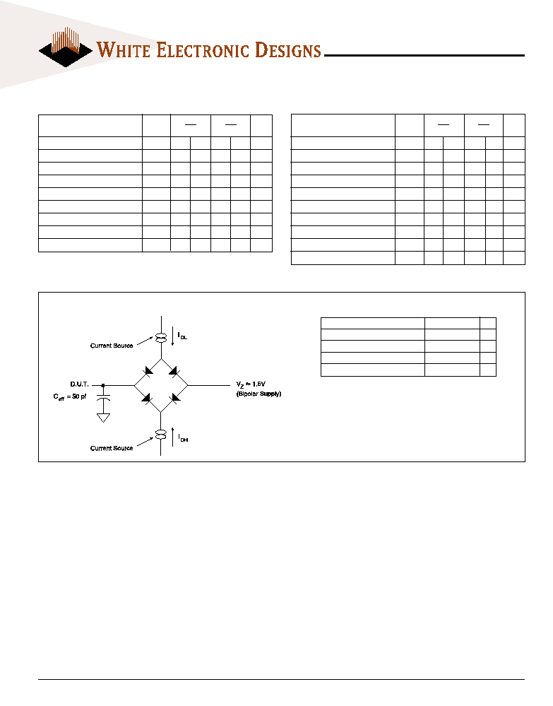
Notes:
VZ is programmable from -2V to +7V.
IOL & IOH programmable from 0 to 16mA.
Tester Impedance Z0 = 75
W.
VZ is typically the midpoint of VOH and VOL.
IOL & IOH
are adjusted to simulate a typical resistive load circuit.
ATE tester includes jig capacitance.
F
IG
. 3 AC T
EST
C
IRCUIT
AC T
EST
C
ONDITIONS
Parameter
Typ
Unit
Input Pulse Levels
V
IL
= 0, V
IH
= 3.0
V
Input Rise and Fall
5
ns
Input and Output Reference Level
1.5
V
Output Timing Reference Level
1.5
V
1. This parameter is guaranteed by design but not tested.
1. This parameter is guaranteed by design but not tested.
5
White Electronic Designs Corporation ∑ (602) 437-1520 ∑ www.whiteedc.com
WSF128K16-XXX
F
IG
. 4 SRAM T
IMING
W
AVEFORM
- R
EAD
C
YCLE
F
IG
. 5 SRAM W
RITE
C
YCLE
- SWE C
ONTROLLED
WS32K32-XHX
F
IG
. 6 SRAM W
RITE
C
YCLE
- SCS C
ONTROLLED

6
White Electronic Designs Corporation ∑ Phoenix AZ ∑ (602) 437-1520
WSF128K16-XXX
F
LASH
AC C
HARACTERISTICS
W
RITE
/E
RASE
/P
ROGRAM
O
PERATIONS
, FWE C
ONTROLLED
(VCC
= 5.0V, TA
= -55∞C
TO
+125∞C)
Parameter
Symbol
-70
-120
Unit
Min
Max
Min
Max
Write Cycle Time
t
AVAV
t
WC
70
120
ns
Chip Select Setup Time
t
E L W L
t
CS
0
0
ns
Write Enable Pulse Width
t
WLWH
t
WP
35
50
ns
Address Setup Time
t
A V W L
t
AS
0
0
ns
Data Setup Time
t
DVWH
t
DS
30
50
ns
Data Hold Time
t
WHDX
t
DH
0
0
ns
Address Hold Time
t
W L A X
t
AH
45
50
ns
Chip Select Hold Time
t
WHEH
t
CH
0
0
ns
Write Enable Pulse Width High
t
WHWL
t
WPH
20
20
ns
Duration of Byte Programming Operation (min)
t
WHWH1
14
14
µs
Chip and Sector Erase Time
t
WHWH2
2.2
60
2.2
60
sec
Read Recovery Time Before Write
t
G H W L
0
0
µs
V
CC
Set-up Time
t
VCS
50
50
µs
Chip Programming Time
12.5
12.5
sec
Output Enable Setup Time
t
OES
0
0
ns
Output Enable Hold Time (1)
t
OEH
10
10
ns
F
LASH
AC C
HARACTERISTICS
R
EAD
O
NLY
O
PERATIONS
(VCC
= 5.0V, TA
= -55∞C
TO
+125∞C)
Parameter
Symbol
-70
-120
Unit
Min
Max
Min
Max
Read Cycle Time
t
AVAV
t
RC
70
120
ns
Address Access Time
t
AVQV
t
ACC
70
120
ns
Chip Select Access Time
t
ELQV
t
CE
70
120
ns
OE to Output Valid
t
GLQV
t
OE
35
50
ns
Chip Select to Output High Z (1)
t
EHQZ
t
DF
20
30
ns
OE High to Output High Z (1)
t
GHQZ
t
DF
20
30
ns
Output Hold from Address, CS or OE Change, whichever is first
t
AXQX
t
OH
0
0
ns
1. Guaranteed by design, not tested.
1. For Toggle and Data Polling.
7
White Electronic Designs Corporation ∑ (602) 437-1520 ∑ www.whiteedc.com
WSF128K16-XXX
Parameter
Symbol
-70
-120
Unit
Min
Max
Min
Max
Write Cycle Time
t
AVAV
t
WC
70
120
ns
FWE Setup Time
t
W L E L
t
WS
0
0
ns
FCS Pulse Width
t
ELEH
t
CP
35
50
ns
Address Setup Time
t
AVEL
t
AS
0
0
ns
Data Setup Time
t
DVEH
t
DS
30
50
ns
Data Hold Time
t
EHDX
t
DH
0
0
ns
Address Hold Time
t
E L A X
t
AH
45
50
ns
FWE Hold from FWE High
t
EHWH
t
WH
0
0
ns
FCS Pulse Width High
t
EHEL
t
CPH
20
20
ns
Duration of Programming Operation
t
WHWH1
14
14
µs
Duration of Erase Operation
t
WHWH2
2.2
60
2.2
60
sec
Read Recovery before Write
t
GHEL
0
0
ns
Chip Programming Time
12.5
12.5
sec
F
LASH
AC C
HARACTERISTICS
W
RITE
/E
RASE
/P
ROGRAM
O
PERATIONS
, FCS C
ONTROLLED
(VCC
= 5.0V, TA
= -55∞C
TO
+125∞C)

8
White Electronic Designs Corporation ∑ Phoenix AZ ∑ (602) 437-1520
WSF128K16-XXX
FIG. 7 AC W
AVEFORMS
F
OR
F
LASH
M
EMORY
R
EAD
O
PERATIONS
9
White Electronic Designs Corporation ∑ (602) 437-1520 ∑ www.whiteedc.com
WSF128K16-XXX
F
IG
. 8 W
RITE
/E
RASE
/P
ROGRAM
O
PERATION
, F
LASH
M
EMORY
FWE C
ONTROLLED
NOTES:
1. PA is the address of the memory location
to be programmed.
2. PD is the data to be programmed at byte address.
3. D7 is the output of the complement of the
data written to the device.
4. DOUT is the output of the data written to
the device.
5. Figure indicates last two bus cycles of four bus
cycle sequence.
10
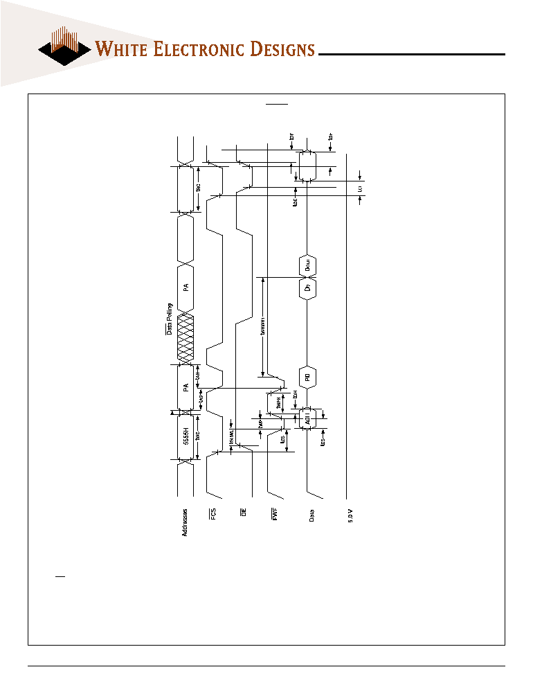
White Electronic Designs Corporation ∑ Phoenix AZ ∑ (602) 437-1520
WSF128K16-XXX
F
IG
. 9 AC W
AVEFORMS
C
HIP
/S
ECTOR
E
RASE
O
PERATIONS
F
OR
F
LASH
M
EMORY
Notes:
1. SA is the sector address
for Sector Erase.

11
White Electronic Designs Corporation ∑ (602) 437-1520 ∑ www.whiteedc.com
WSF128K16-XXX
F
IG
. 10 AC W
AVEFORMS
F
OR
D
ATA
P
OLLING
D
URING
E
MBEDDED
A
LGORITHM
O
PERATIONS
F
OR
F
LASH
M
EMORY
12
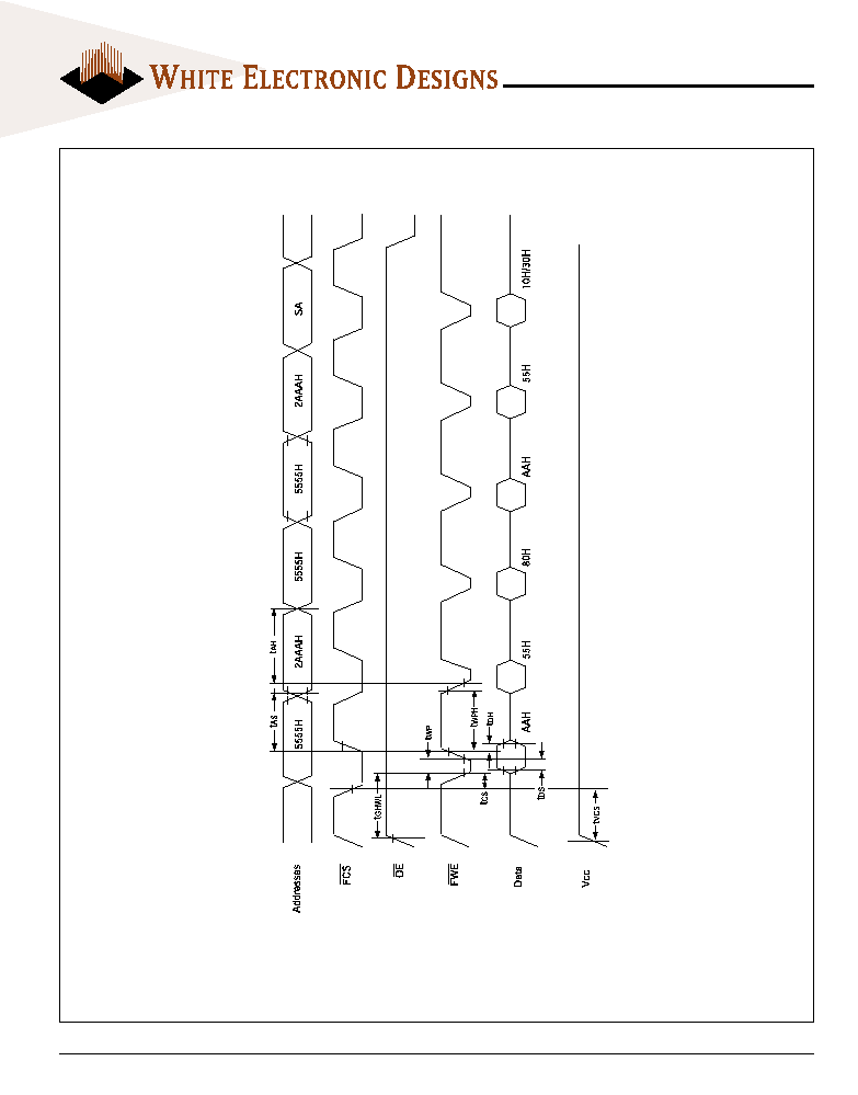
White Electronic Designs Corporation ∑ Phoenix AZ ∑ (602) 437-1520
WSF128K16-XXX
F
IG
. 11 W
RITE
/E
RASE
/P
ROGRAM
O
PERATION
F
OR
F
LASH
M
EMORY
, CS
CONTROLLED
NOTES:
1. PA represents the address of the memory location to be programmed.
2. PD represents the data to be programmed at byte address.
3. D7 is the output of the complement of the data written to the device.
4. DOUT is the output of the data written to the device.
5. Figure indicates the last two bus cycles of a four bus cycle sequence.
13
White Electronic Designs Corporation ∑ (602) 437-1520 ∑ www.whiteedc.com
WSF128K16-XXX
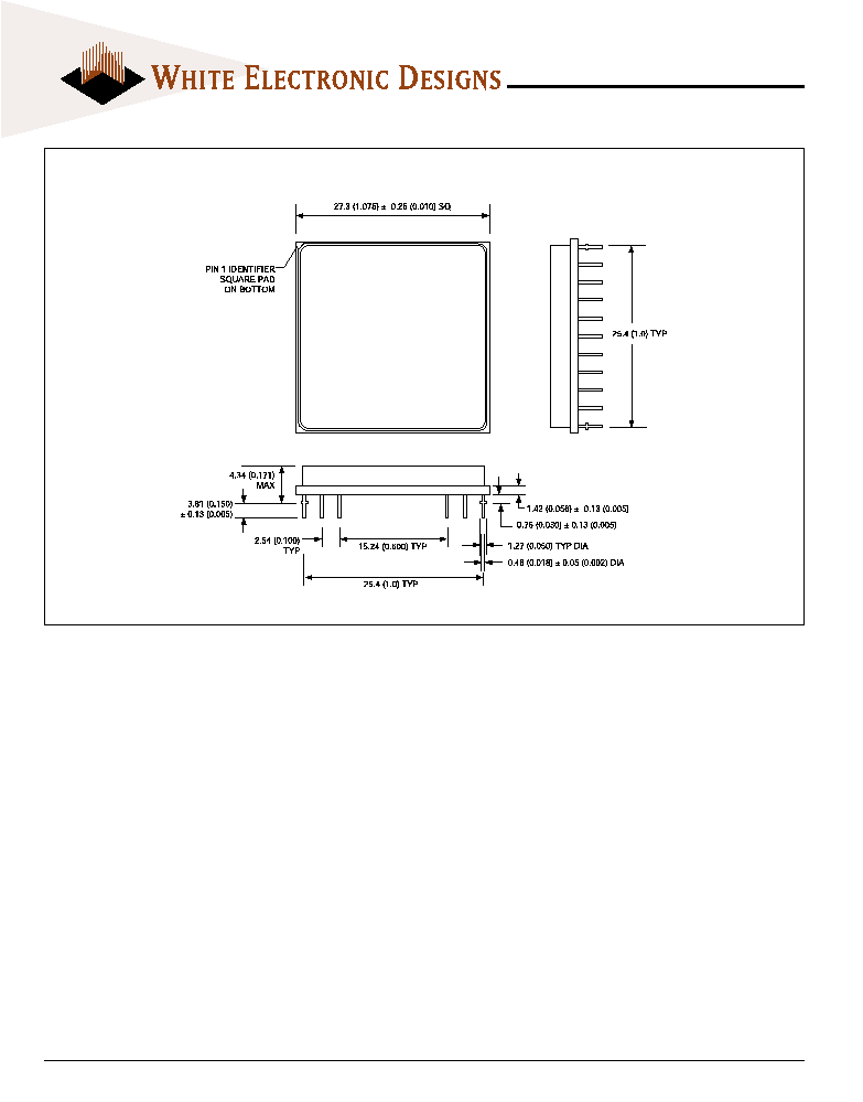
P
ACKAGE
400: 66 P
IN
, PGA T
YPE
, C
ERAMIC
H
EX
-I
N
-L
INE
P
ACKAGE
, H
IP
(H1)
ALL LINEAR DIMENSIONS ARE MILLIMETERS AND PARENTHETICALLY IN INCHES
14
White Electronic Designs Corporation ∑ Phoenix AZ ∑ (602) 437-1520
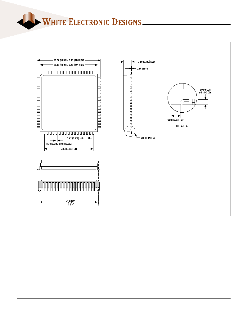
WSF128K16-XXX
P
ACKAGE
519: 68 L
EAD
, C
ERAMIC
Q
UAD
F
LAT
P
ACK
, CQFP (G1U)
ALL LINEAR DIMENSIONS ARE MILLIMETERS AND PARENTHETICALLY IN INCHES
The WEDC 68 lead G1U CQFP
fills the same fit and function
as the JEDEC 68 lead CQFJ or
68 PLCC. But the G1U has the
TCE and lead inspection
advantage of the CQFP form.
15
White Electronic Designs Corporation ∑ (602) 437-1520 ∑ www.whiteedc.com
WSF128K16-XXX
LEAD FINISH:
Blank =Gold plated leads
A
= Solder dip leads
DEVICE GRADE:
M
= Military Screened
-55∞C to +125∞C
I
= Industrial
-40∞C to +85∞C
C
= Commercial
0∞C to +70∞C
PACKAGE TYPE:
H1
= 1.075" sq. Ceramic Hex In-line Package, HIP (Package 400)
H
= 1.185" sq. Ceramic Hex In-line Package, HIP (Package 401)
G1U
= 22.4 mm Ceramic Quad Flat Pack, CQFP (Package 519)
ACCESS TIME (ns)
37
= 35ns SRAM and 70ns FLASH
72
= 70ns SRAM and 120ns FLASH
ORGANIZATION, 128K x 16
FLASH
SRAM
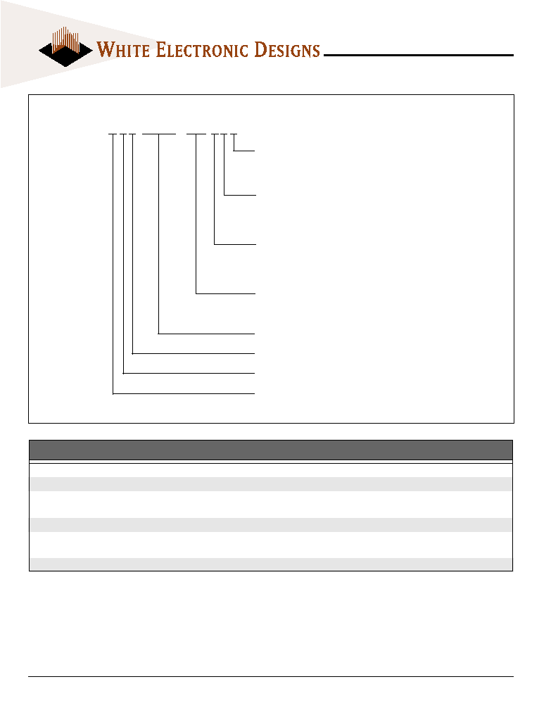
WHITE ELECTRONIC DESIGNS CORP.
O
RDERING
I
NFORMATION
W S F 128K16 - XXX X X X
DEVICE TYPE
SRAM SPEED
FLASH SPEED
PACKAGE
SMD NO.
128K x 16 Mixed Module
70ns
120ns
66 pin HIP (H)
5962-96900 01HXX
128K x 16 Mixed Module
70ns
120ns
66 pin HIP (H1)
5962-96900 01HYX
128K x 16 Mixed Module
35ns
70ns
66 pin HIP (H)
5962-96900 02HXX
128K x 16 Mixed Module
35ns
70ns
66 pin HIP (H1)
5962-96900 02HYX
128K x 16 Mixed Module
70ns
120ns
68 lead CQFP/J (G1U)
5962-96900 01HX*
128K x 16 Mixed Module
35ns
70ns
68 lead CQFP/J (G1U)
5962-96900 02HX*
*SMD Pending