
1
White Electronic Designs Corporation ∑ (602) 437-1520 ∑ www.wedc.com
White Electronic Designs
WSF512K32-XXX
May 2006
Rev. 9
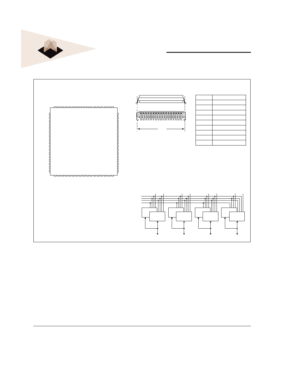
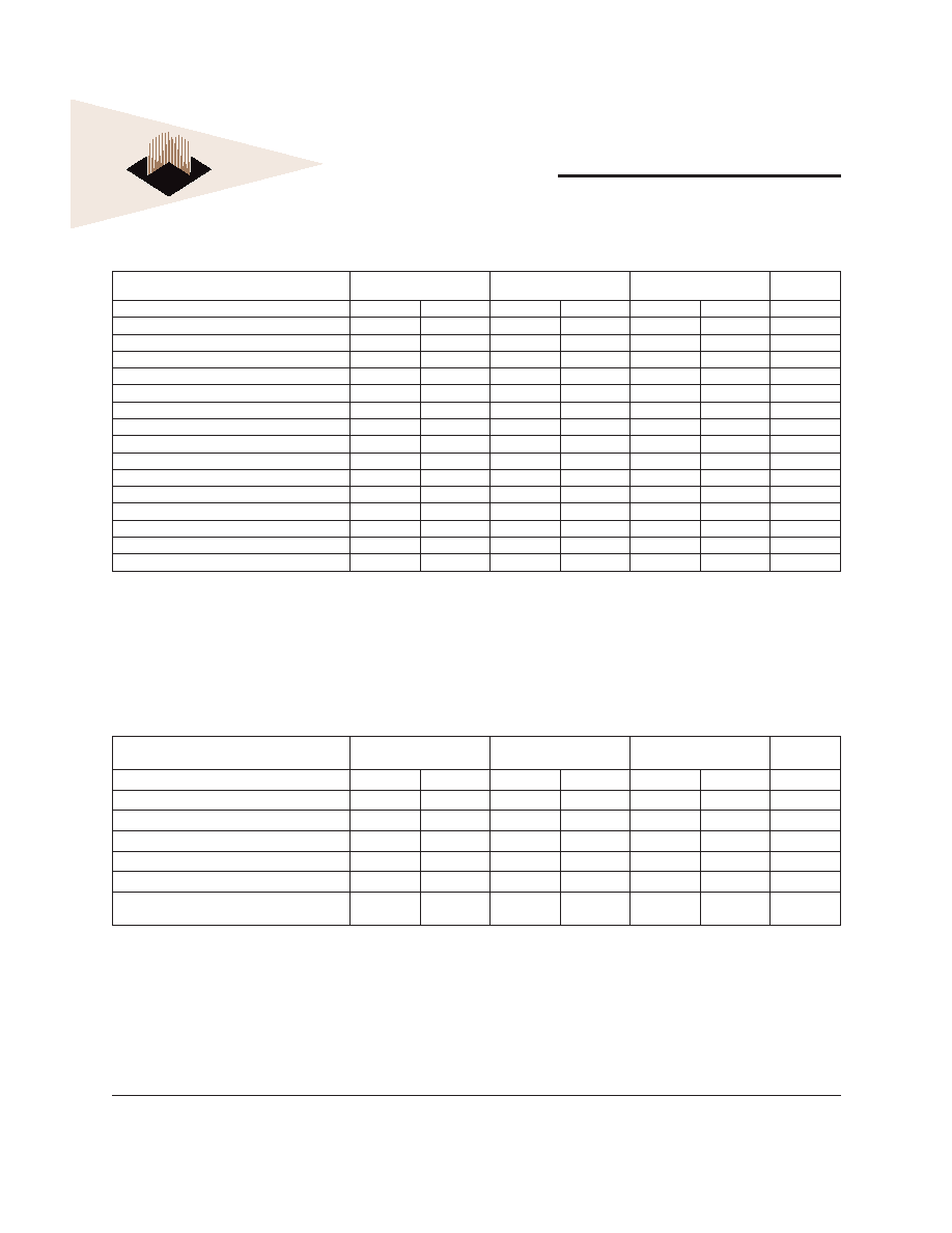
I/O8
I/O9
I/O10
A14
A16
A11
A0
A18
I/O0
I/O1
I/O2
FWE2#
SWE2#
GND
I/O11
A10
A9
A15
VCC
FCS#
SCS#
I/O3
I/O15
I/O14
I/O13
I/O12
OE#
A17
FWE1#
I/O7
I/O6
I/O5
I/O4
I/O24
I/O25
I/O26
A7
A12
SWE1#
A13
A8
I/O16
I/O17
I/O18
VCC
SWE4#
FWE4#
I/O27
A4
A5
A6
FWE3#
SWE3#
GND
I/O19
I/O31
I/O30
I/O29
I/O28
A1
A2
A3
I/O23
I/O22
I/O21
I/O20
11 22 33 44 55 66
1 12 23 34 45 56
512K
X
32 SRAM / FLASH MODULE
Built in Decoupling Caps and Multiple Ground Pins
for Low Noise Operation
Weight - 13 grams typical
FLASH MEMORY FEATURES
100,000 Erase/Program Cycles
Sector
Architecture
∑ 8 equal size sectors of 64KBytes each
∑ Any combination of sectors can be concurrently
erased. Also supports full chip erase
5 Volt Programming; 5V ± 10% Supply
Embedded Erase and Program Algorithms
Hardware Write Protection
Page Program Operation and Internal Program
Control Time.
* This product is subject to change without notice.
Note: Programming information available upon request.
Figure 1 ≠ PIN CONFIGURATION FOR WSF512K32-29H2X
Block Diagram
Pin Description
I/O0-31
Data Inputs/Outputs
A0-18
Address Inputs
SWE1-4#
SRAM Write Enables
SCS#
SRAM Chip Select
OE#
Output Enable
VCC
Power Supply
GND
Ground
NC Not
Connected
FWE1-4#
Flash Write Enables
FCS#
Flash Chip Select
O E #
F C S #
S C S #
A 0 - 1 8
F W E
1
# S W E
1
#
512K x 8 Flash
512K x 8 SRAM
I/O0-7
F W E
2
# S W E
2
#
512K x 8 Flash
512K x 8 SRAM
I/O8-15
F W E
3
# S W E
3
#
512K x 8 Flash
512K x 8 SRAM
I/O16-23
F W E
4
# S W E
4
#
512K x 8 Flash
512K x 8 SRAM
I/O24-31
FEATURES
Access Times of 25ns (SRAM) and 70, 90ns
(FLASH)
Packaging
∑ 66 pin, PGA Type, 1.385" square HIP, Hermetic
Ceramic HIP (Package 402)
∑ 68 lead, Hermetic CQFP (G2T), 22.4mm (0.880")
square (Package 509) 4.57mm (0.180") height.
Designed to fi t JEDEC 68 lead 0.990" CQFJ
footprint (Figure 2). Package to be developed.
512Kx32
SRAM
512Kx32
5V
Flash
Organized as 512Kx32 of SRAM and 512Kx32 of
Flash Memory with common Data Bus
Low Power CMOS
Commercial, Industrial and Military Temperature
Ranges
TTL Compatible Inputs and Outputs
Top View
2
White Electronic Designs Corporation ∑ (602) 437-1520 ∑ www.wedc.com
White Electronic Designs
WSF512K32-XXX
May 2006
Rev. 9
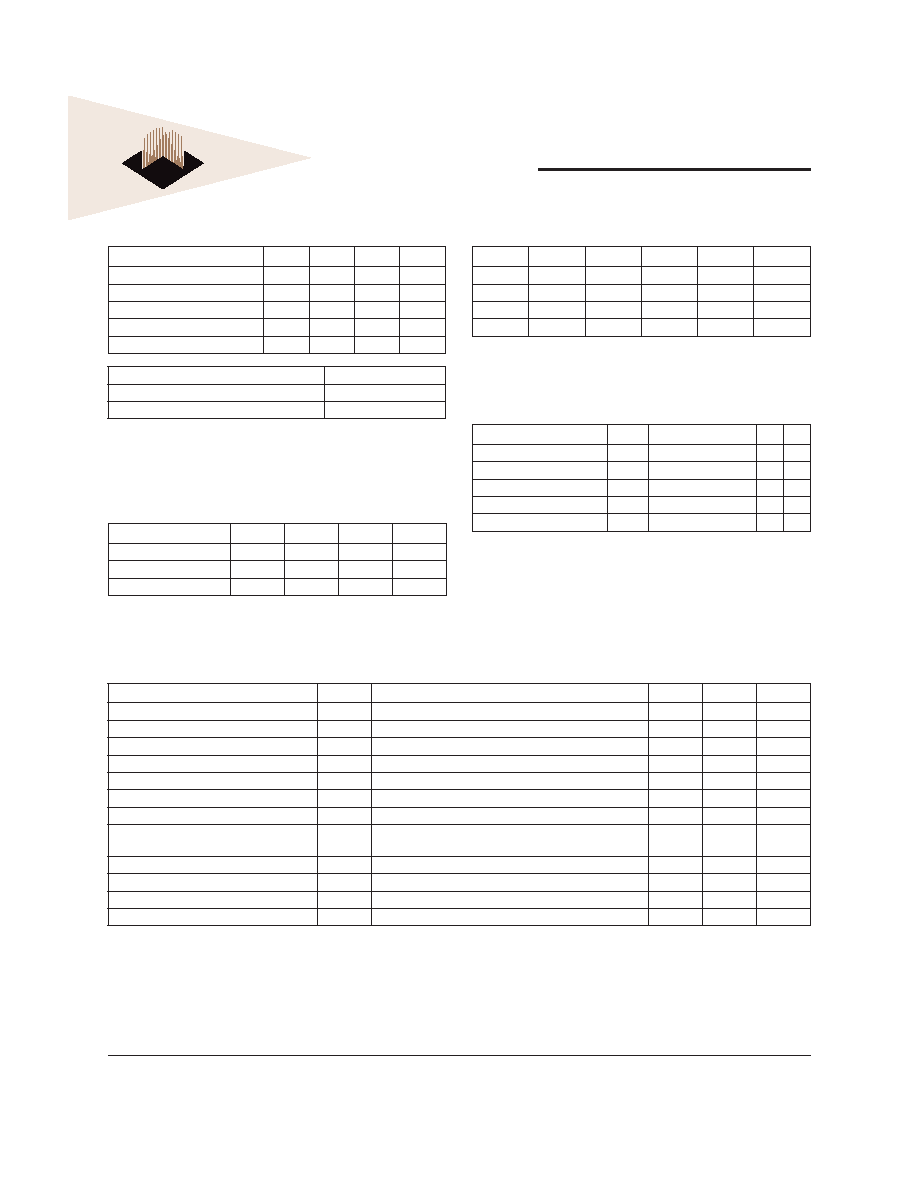
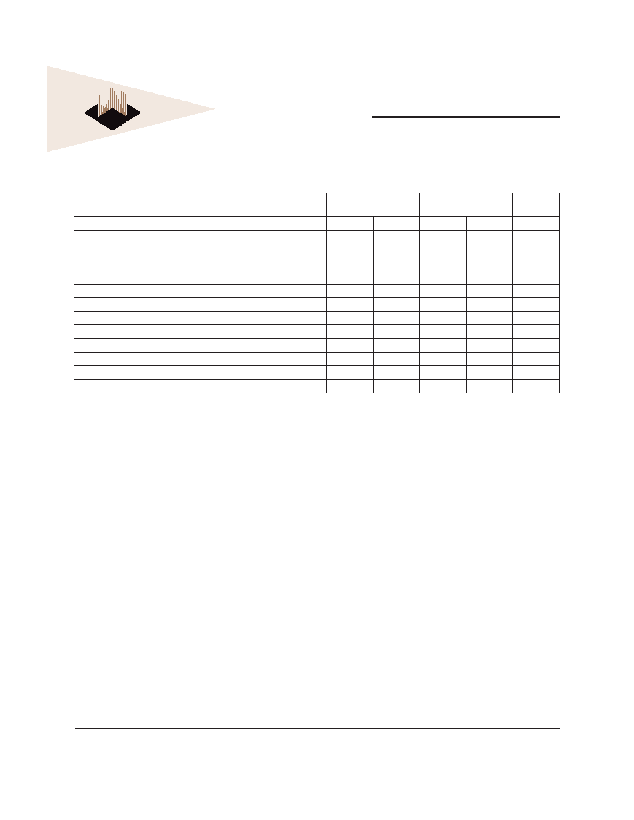
FIGURE 2 ≠ PIN CONFIGURATION FOR WSF512K32-29G2TX
Block Diagram
Pin Description
O E #
F C S #
S C S #
A 0 - 1 8
F W E
1
# S W E
1
#
512K x 8 Flash
512K x 8 SRAM
I/O0-7
F W E
2
# S W E
2
#
512K x 8 Flash
512K x 8 SRAM
I/O8-15
F W E
3
# S W E
3
#
512K x 8 Flash
512K x 8 SRAM
I/O16-23
F W E
4
# S W E
4
#
512K x 8 Flash
512K x 8 SRAM
I/O24-31
Top View
10
11
12
13
14
15
16
17
18
19
20
21
22
23
24
25
26
60
59
58
57
56
55
54
53
52
51
50
49
48
47
46
45
44
9 8 7 6 5 4 3 2 1 68 67 66 65 64 63 62 61
27 28 29 30 31 32 33 34 35 36 37 38 39 40 41 42 43
I/O
0
I/O
1
I/O
2
I/O
3
I/O
4
I/O
5
I/O
6
I/O
7
GND
I/O
8
I/O
9
I/O
10
I/O
11
I/O
12
I/O
13
I/O
14
I/O
15
V
CC
A
11
A
12
A
13
A
14
A
15
A
16
FCS
#
OE
#
SWE
2
#
A
17
FWE
2
#
FWE
3
#
FWE
4
#
A
18
SCS
#
SWE
1
#
I/O
16
I/O
17
I/O
18
I/O
19
I/O
20
I/O
21
I/O
22
I/O
23
GND
I/O
24
I/O
25
I/O
26
I/O
27
I/O
28
I/O
29
I/O
30
I/O
31
NC
A
0
A
1
A
2
A
3
A
4
A
5
SWE
3
#
GND
SWE
4
#
FWE
1
#
A
6
A
7
A
8
A
9
A
10
V
CC
The WEDC 68 lead G2T
CQFP fi lls the same fi t and
function as the JEDEC 68
lead CQFJ or 68 PLCC. But
the G2T has the TCE and
lead inspection advantage of
the CQFP form.
0.940"
I/O0-31
Data Inputs/Outputs
A0-18
Address Inputs
SWE1-4#
SRAM Write Enables
SCS#
SRAM Chip Select
OE#
Output Enable
VCC
Power Supply
GND
Ground
NC Not
Connected
FWE1-4#
Flash Write Enables
FCS#
Flash Chip Select
3
White Electronic Designs Corporation ∑ (602) 437-1520 ∑ www.wedc.com
White Electronic Designs
WSF512K32-XXX
May 2006
Rev. 9
SRAM TRUTH TABLE
SCS#
OE#
SWE#
Mode
Data I/O
Power
H
X
X
Standby
High Z
Standby
L
L
H
Read
Data Out
Active
L
H
H
Read
High Z
Active
L
X
L
Write
Data In
Active
NOTE:
1. FCS# must remain high when SCS# is low.
ABSOLUTE MAXIMUM RATINGS
Parameter
Symbol
Min
Max
Unit
Operating Temperature
T
A
-55 +125
∞C
Storage Temperature
T
STG
-65
+150
∞C
Signal Voltage Relative to GND
V
G
-0.5
7.0
V
Junction Temperature
T
J
150
∞C
Supply Voltage
V
CC
-0.5
7.0
V
Parameter
Flash Data Retention
20 years
Flash Endurance (write/erase cycles)
100,000
NOTE:
1. Stresses above the absolute maximum rating may cause permanent damage to the
device. Extended operation at the maximum levels may degrade performance and
affect reliability.
RECOMMENDED OPERATING CONDITIONS
Parameter
Symbol
Min
Max
Unit
Supply Voltage
V
CC
4.5
5.5
V
Input High Voltage
V
IH
2.2
V
CC
+ 0.3
V
Input Low Voltage
V
IL
-0.5
+0.8
V
CAPACITANCE
Ta = +25∞C
Parameter
Symbol
Conditions Max Unit
OE# capacitance
C
OE
V
IN
= 0 V, f = 1.0 MHz
80
pF
F/S WE
1-4
# capacitance
C
WE
V
IN
= 0 V, f = 1.0 MHz
30
pF
F/S CS# capacitance
C
CS
V
IN
= 0 V, f = 1.0 MHz
50
pF
D
0-31
capacitance
C
I/O
V
I/O
= 0 V, f = 1.0 MHz
30
pF
A
0-18
capacitance
C
AD
V
IN
= 0 V, f = 1.0 MHz
80
pF
This parameter is guaranteed by design but not tested.
DC CHARACTERISTICS
V
CC
= 5.0V, V
SS
= 0V, -55∞C T
A
+125∞C
Parameter
Symbol
Conditions
Min
Max
Unit
Input Leakage Current
I
LI
V
CC
= 5.5, V
IN
= GND to V
CC
10
µA
Output Leakage Current
I
LO
SCS# = V
IH
, OE# = V
IH
, V
OUT
= GND to V
CC
10
µA
SRAM Operating Supply Current x 32 Mode
I
CCx32
SCS# = V
IL
, OE# = FCS# = V
IH
, f = 5MHz, V
CC
= 5.5
550
mA
Standby Current
I
SB
FCS# = SCS# = V
IH
, OE# = V
IH
, f = 5MHz, V
CC
= 5.5
90
mA
SRAM Output Low Voltage
V
OL
I
OL
= 6mA, V
CC
= 4.5
0.4
V
SRAM Output High Voltage
V
OH
I
OH
= -4.0mA, V
CC
= 4.5
2.4
V
Flash V
CC
Active Current for Read (1)
I
CC1
FCS# = V
IL
, OE# = SCS# = V
IH
250
mA
Flash V
CC
Active Current for Program or
Erase (2)
I
CC2
FCS# = V
IL
, OE# = SCS# = V
IH
300
mA
Flash Output Low Voltage
V
OL
I
OL
= 8.0mA, V
CC
= 4.5
0.45
V
Flash Output High Voltage
V
OH1
I
OH
= -2.5 mA, V
CC
= 4.5
0.85 x V
CC
V
Flash Output High Voltage
V
OH2
I
OH
= -100 µA, V
CC
= 4.5
V
CC
-0.4
V
Flash Low V
CC
Lock Out Voltage
V
LKO
3.2
4.2
V
NOTES:
1. The I
CC
current listed includes both the DC operating current and the frequency dependent component (@ 5 MHz).
The frequency component typically is less than 2mA/MHz, with OE# at V
IH
.
2. I
CC
active while Embedded Algorithm (program or erase) is in progress.
3. DC test conditions: V
IL
= 0.3V, V
IH
= V
CC
- 0.3V
4
White Electronic Designs Corporation ∑ (602) 437-1520 ∑ www.wedc.com
White Electronic Designs
WSF512K32-XXX
May 2006
Rev. 9
I
Current Source
D.U.T.
C = 50 pf
eff
I
OL
V
1.5V
(Bipolar Supply)
Z
Current Source
OH
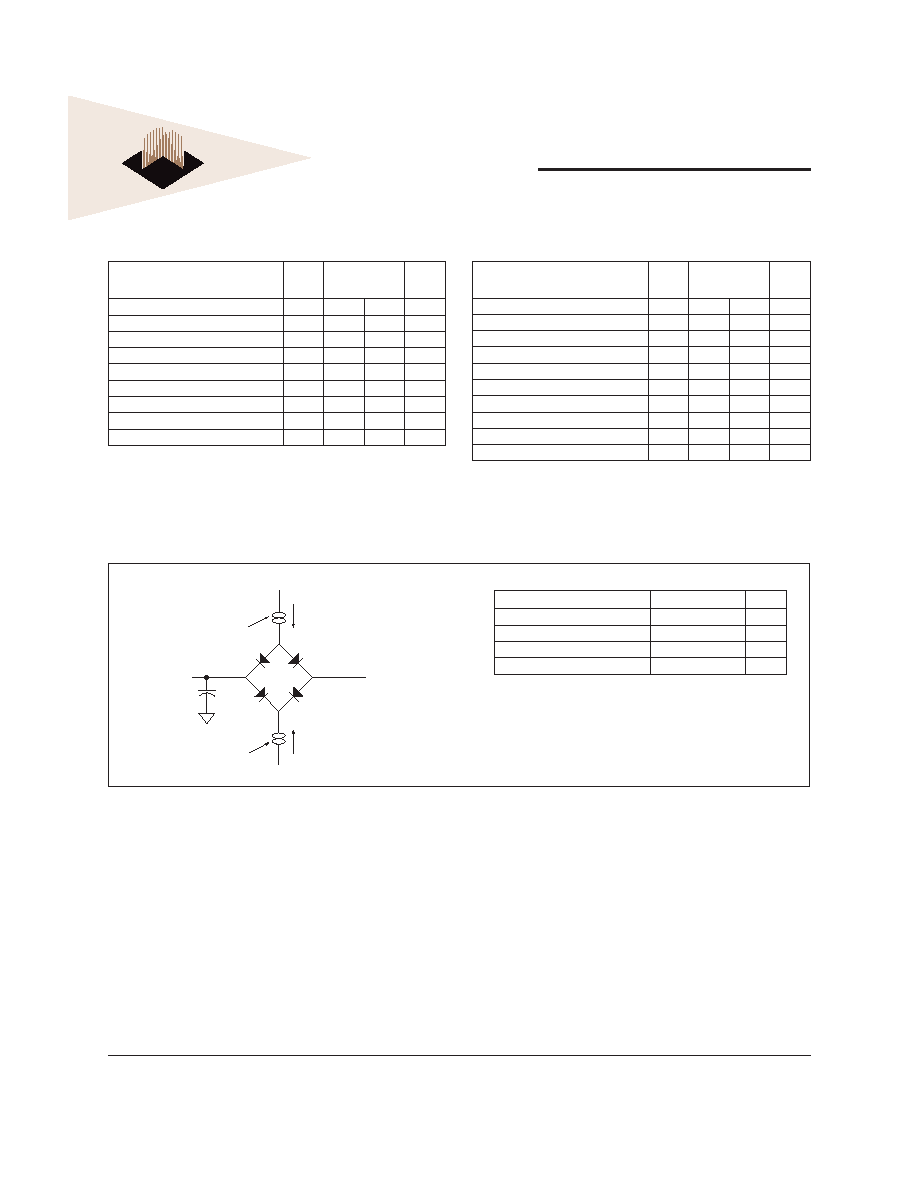
FIGURE 3 AC TEST CIRCUIT
SRAM AC CHARACTERISTICS
V
CC
= 5.0V, -55∞C T
A
+125∞C
Parameter
Read Cycle
Symbol
-25
Units
Min
Max
Read Cycle Time
t
RC
25
ns
Address Access Time
t
AA
25
ns
Output Hold from Address Change
t
OH
0
ns
Chip Select Access Time
t
ACS
25
ns
Output Enable to Output Valid
t
OE
15
ns
Chip Select to Output in Low Z
t
CLZ
1
3
ns
Output Enable to Output in Low Z
t
OLZ
1
0
ns
Chip Disable to Output in High Z
t
CHZ
1
12
ns
Output Disable to Output in High Z
t
OHZ
1
12
ns
1. This parameter is guaranteed by design but not tested.
SRAM AC CHARACTERISTICS
V
CC
= 5.0V, -55∞C T
A
+125∞C
Parameter
Write Cycle
Symbol
-25
Units
Min
Max
Write Cycle Time
t
WC
25
ns
Chip Select to End of Write
t
CW
20
ns
Address Valid to End of Write
t
AW
20
ns
Data Valid to End of Write
t
DW
15
ns
Write Pulse Width
t
WP
20
ns
Address Setup Time
t
AS
3
ns
Address Hold Time
t
AH
0
ns
Output Active from End of Write
t
OW
1
3
ns
Write Enable to Output in High Z
t
WHZ
1
15
ns
Data Hold from Write Time
t
DH
0
ns
1. This parameter is guaranteed by design but not tested.
AC Test Conditions
Parameter
Typ
Unit
Input Pulse Levels
V
IL
= 0, V
IH
= 3.0
V
Input Rise and Fall
5
ns
Input and Output Reference Level
1.5
V
Output Timing Reference Level
1.5
V
Notes:
V
Z
is programmable from -2V to +7V.
I
OL
& I
OH
programmable from 0 to 16mA.
Tester Impedance Z0 = 75 .
V
Z
is typically the midpoint of V
OH
and V
OL
.
I
OL
& I
OH
are adjusted to simulate a typical resistive load circuit.
ATE tester includes jig capacitance.
5
White Electronic Designs Corporation ∑ (602) 437-1520 ∑ www.wedc.com
White Electronic Designs
WSF512K32-XXX
May 2006
Rev. 9
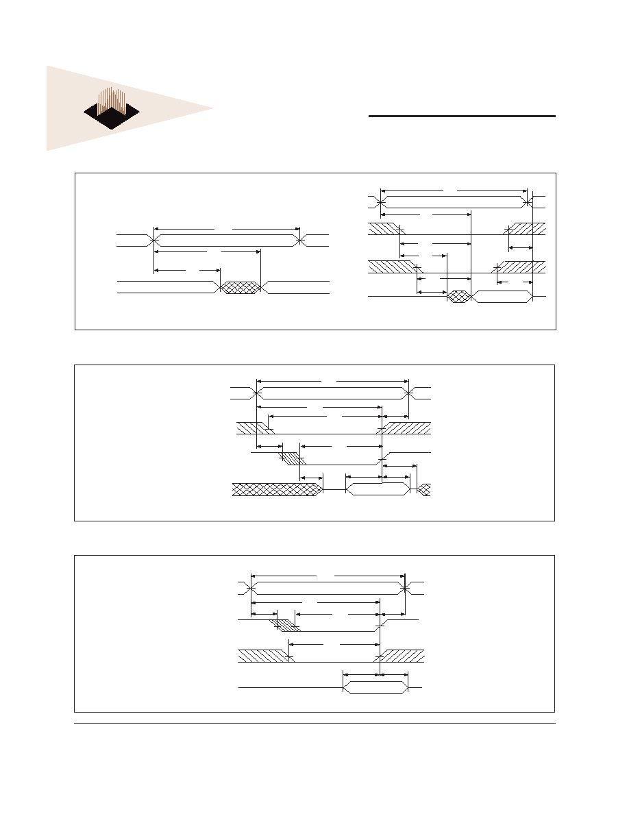
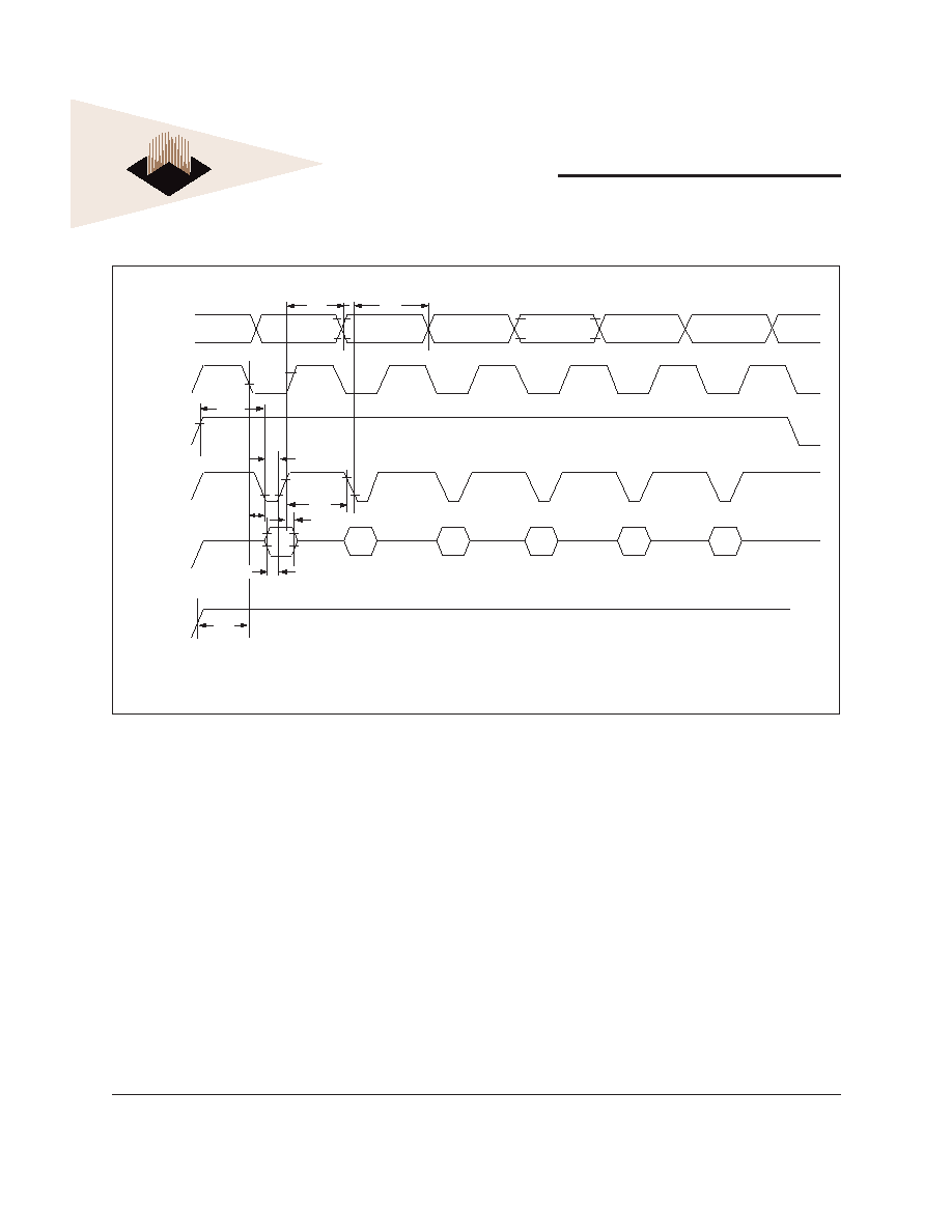
ADDRESS
DATA I/O
t
AW
t
AS
t
CW
t
AH
t
WP
t
DH
t
DW
t
WC
SCS#
SWE#
DATA VALID
FIGURE 4 ≠ SRAM TIMING WAVEFORM - READ CYCLE
FIGURE 5 ≠ SRAM WRITE CYCLE - SWE# CONTROLLED
FIGURE 6 ≠ SRAM WRITE CYCLE - SCS# CONTROLLED
ADDRESS
DATA I/O
t
AA
t
OH
t
RC
DATA VALID
PREVIOUS DATA VALID
READ CYCLE 1, (SCS# = OE# = V
IL
, SWE# = FCS# = V
IH
)
READ CYCLE 2, (SWE# = FCS# = V
IH
)
WRITE CYCLE 2, SCS# CONTROLLED (FCS# = V
IH
)
WRITE CYCLE 1, SWE# CONTROLLED (FCS# = V
IH
)
ADDRESS
DATA I/O
t
AA
t
ACS
t
OE
t
CLZ
t
OLZ
t
OHZ
t
RC
DATA VALID
HIGH IMPEDANCE
SCS#
SOE#
t
CHZ
ADDRESS
DATA I/O
t
AW
t
CW
t
AH
t
WP
t
DW
t
WHZ
t
AS
t
OW
t
DH
t
WC
DATA VALID
SCS#
SWE#
6
White Electronic Designs Corporation ∑ (602) 437-1520 ∑ www.wedc.com
White Electronic Designs
WSF512K32-XXX
May 2006
Rev. 9
FLASH AC CHARACTERISTICS ≠ WRITE/ERASE/PROGRAM OPERATIONS, FWE# CONTROLLED
V
CC
= 5.0V, -55∞C T
A
+125∞C
Parameter
Symbol
-70
-90
Unit
Min
Max
Min
Max
Write Cycle Time
t
AVAV
t
WC
70
90
ns
Chip Select Setup Time
t
ELWL
t
CS
0
0
ns
Write Enable Pulse Width
t
WLWH
t
WP
45
45
ns
Address Setup Time
t
AVWL
t
AS
0
0
ns
Data Setup Time
t
DVWH
t
DS
45
45
ns
Data Hold Time
t
WHDX
t
DH
0
0
ns
Address Hold Time
t
WLAX
t
AH
45
45
ns
Write Enable Pulse Width High
t
WHWL
t
WPH
20
20
ns
Duration of Byte Programming Operation (1)
t
WHWH1
300
300
µs
Chip and Sector Erase Time (2)
t
WHWH2
15
15
sec
Read Recovery Time Before Write
t
GHWL
0
0
µs
VCC Set-up Time
t
VCS
50
50
µs
Chip Programming Time
11
11
sec
Output Enable Setup Time
t
OES
0
0
ns
Output Enable Hold Time (4)
t
OEH
10
10
ns
Chip Erase Time (3)
64
64
sec
NOTES:
1. Typical value for t
WHWH
1
is 7ns.
2. Typical value for t
WHWH
2
is 1sec.
3. Typical value for Chip Erase Time is 8sec.
4. For Toggle and Data# Polling.
FLASH AC CHARACTERISTICS ≠ READ ONLY OPERATIONS
V
CC
= 5.0V, -55∞C T
A
+125∞C
Parameter
Symbol
-70
-90
Unit
Min
Max
Min
Max
Read Cycle Time
t
AVAV
t
RC
70
90
ns
Address Access Time
t
AVQV
t
ACC
70
90
ns
Chip Select Access Time
t
ELQV
t
CE
70
90
ns
OE# to Output Valid
t
GLQV
t
OE
35
35
ns
Chip Select to Output High Z (1)
t
EHQZ
t
DF
20
20
ns
OE# High to Output High Z (1)
t
GHQZ
t
DF
20
20
ns
Output Hold from Address, FCS# or OE# Change,
whichever is fi rst
t
AXQX
t
OH
0
0
ns
1. Guaranteed by design, not tested.
7
White Electronic Designs Corporation ∑ (602) 437-1520 ∑ www.wedc.com
White Electronic Designs
WSF512K32-XXX
May 2006
Rev. 9
Parameter
Symbol
-70
-90
Unit
Min
Max
Min
Max
Write Cycle Time
t
AVAV
t
WC
70
90
ns
FWE# Setup Time
t
WLEL
t
WS
0
0
ns
FCS# Pulse Width
t
ELEH
t
CP
45
45
ns
Address Setup Time
t
AVEL
t
AS
0
0
ns
Data Setup Time
t
DVEH
t
DS
45
45
ns
Data Hold Time
t
EHDX
t
DH
0
0
ns
Address Hold Time
t
ELAX
t
AH
45
45
ns
FCS# Pulse Width High
t
EHEL
t
CPH
20
20
ns
Duration of Programming Operation (1)
t
WHWH1
300
300
µs
Sector Erase Time (2)
t
WHWH2
15
15
sec
Read Recovery Time
t
GHEL
0
0
ns
Chip Programming Time
11
sec
Chip Erase Time (3)
64
sec
NOTES:
1. Typical value for t
WHWH
1
is 7ns.
2. Typical value for t
WHWH
2
is 1sec.
3. Typical value for Chip Erase Time is 8sec.
FLASH AC CHARACTERISTICS ≠ WRITE/ERASE/PROGRAM OPERATIONS, FCS# CONTROLLED
V
CC
= 5.0V, -55∞C T
A
+125∞C
8
White Electronic Designs Corporation ∑ (602) 437-1520 ∑ www.wedc.com
White Electronic Designs
WSF512K32-XXX
May 2006
Rev. 9
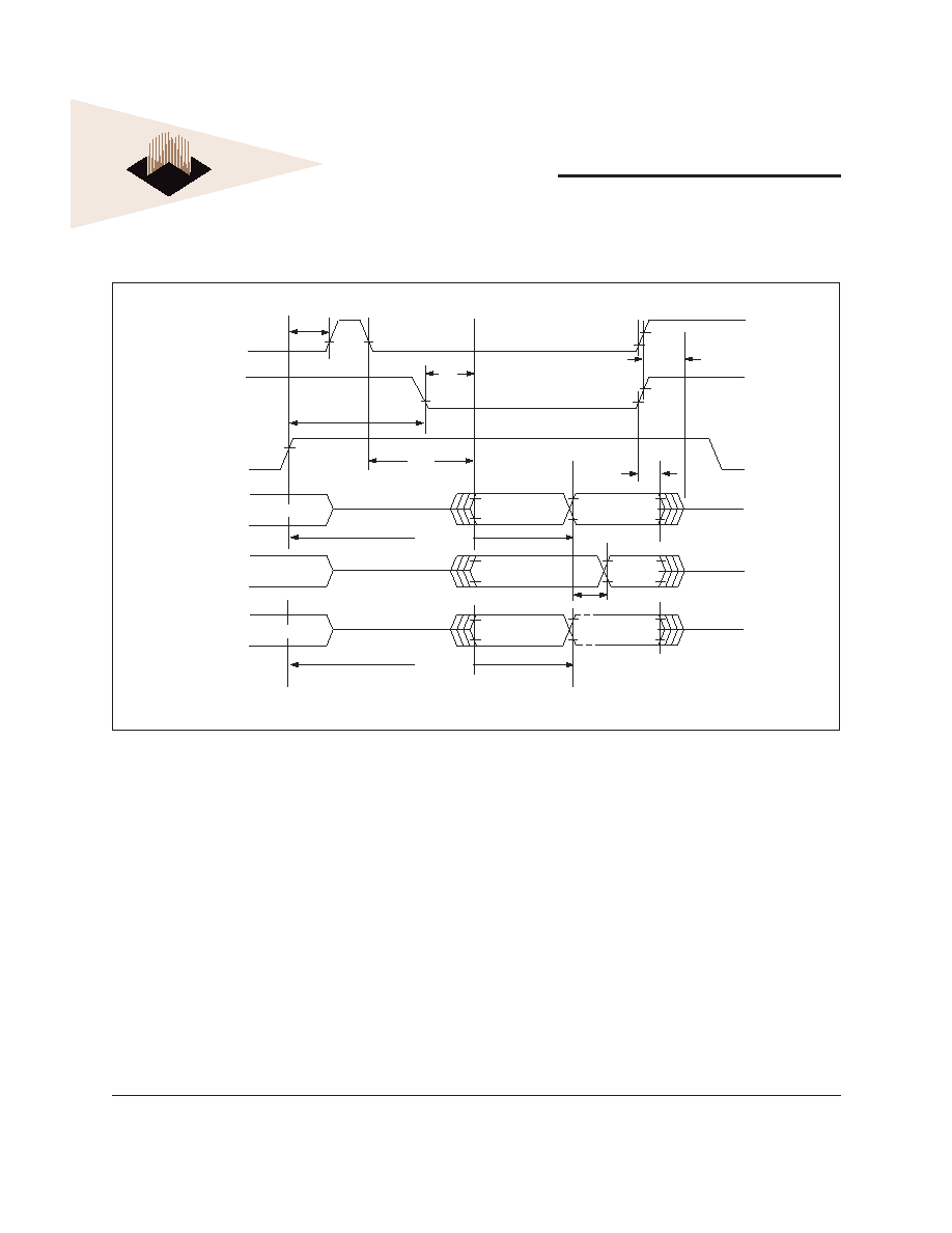
FIGURE 7 ≠ AC WAVEFORMS FOR FLASH MEMORY READ OPERATIONS
Addresses
FCS#
OE#
FWE#
Outputs
High Z
Addresses Stable
t
OE
t
RC
Output Valid
t
CE
t
ACC
t
OH
High Z
t
DF
NOTE: SCS# = V
IH
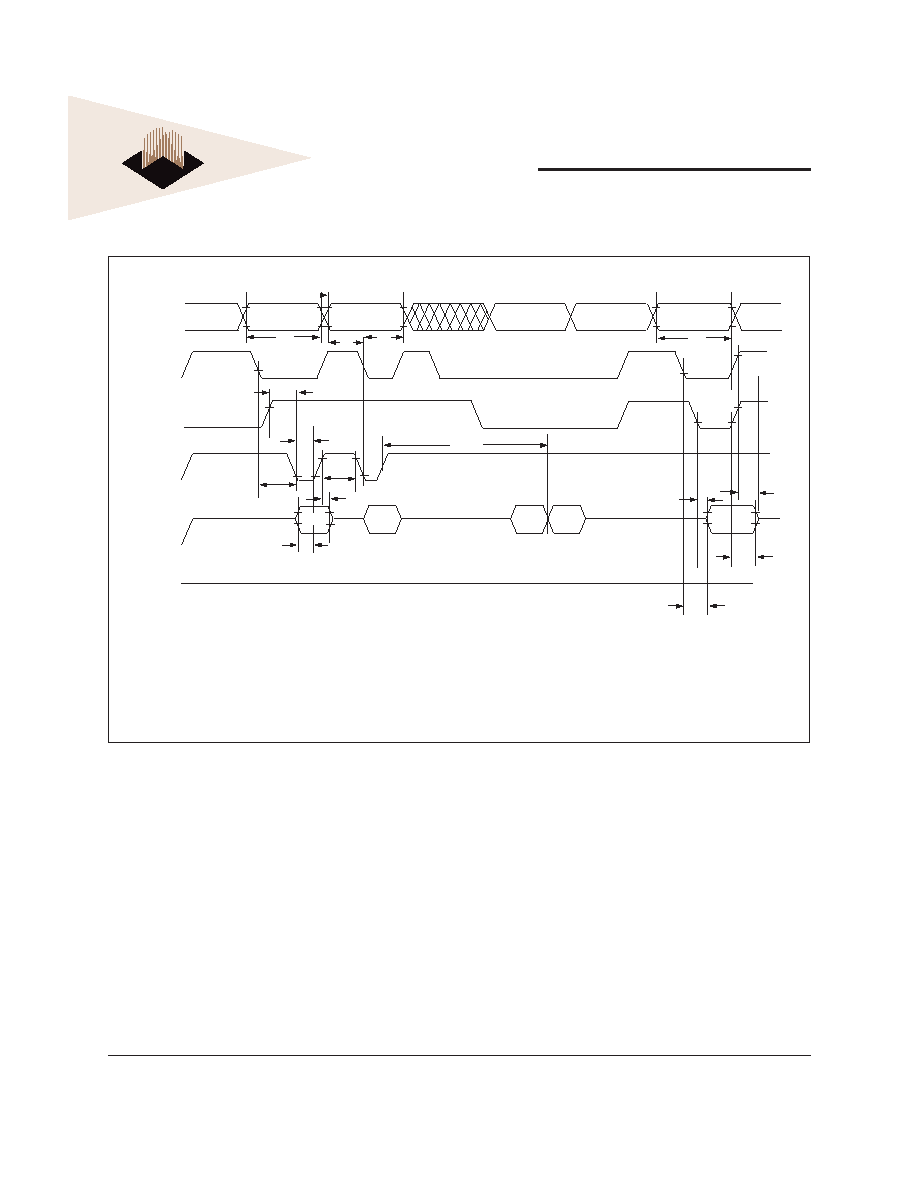
9
White Electronic Designs Corporation ∑ (602) 437-1520 ∑ www.wedc.com
White Electronic Designs
WSF512K32-XXX
May 2006
Rev. 9
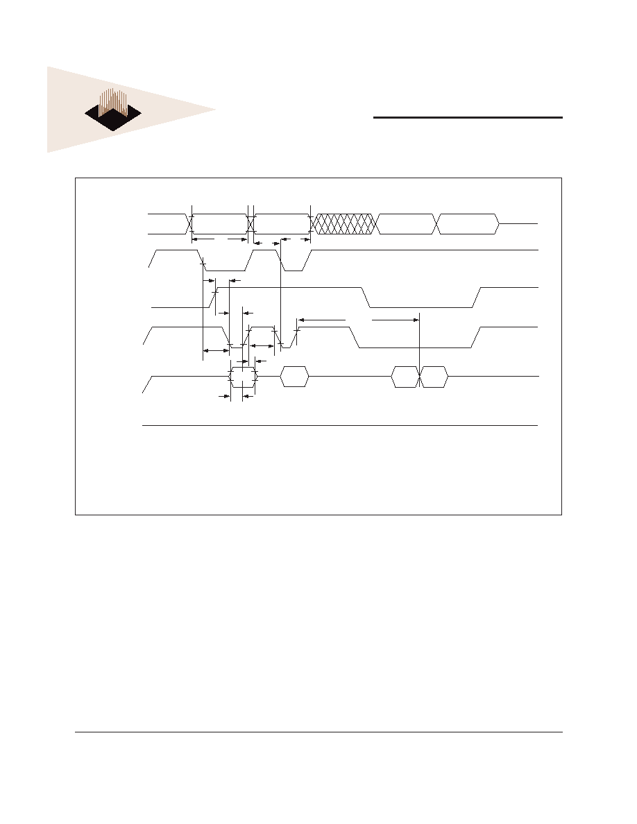
FIGURE 8 ≠ WRITE/ERASE/PROGRAM OPERATION, FLASH MEMORY FWE# CONTROLLED
NOTES:
1. PA is the address of the memory location to be programmed.
2. PD is the data to be programmed at byte address.
3. D7# is the output of the complement of the data written to the device.
4. D
OUT
is the output of the data written to the device.
5. Figure indicates last two bus cycles of four bus cycle sequence.
6. SCS# = V
IH
Addresses
FCS#
OE#
FWE#
Data
5.0 V
5555H
PA
PA
t
WC
t
CS
PD
D
7
#
D
OUT
t
AH
t
WPH
t
DH
t
DS
Data# Polling
t
AS
t
RC
t
WP
A0H
t
OE
t
DF
t
OH
t
CE
t
GHWL
t
WHWH1
10
White Electronic Designs Corporation ∑ (602) 437-1520 ∑ www.wedc.com
White Electronic Designs
WSF512K32-XXX
May 2006
Rev. 9
FIGURE 9 ≠ AC WAVEFORMS CHIP/SECTOR ERASE OPERATIONS FOR FLASH MEMORY
Notes:
1. SA is the sector address for Sector Erase.
2. SCS# = V
IH
Addresses
FCS#
OE#
FWE#
Data
V
CC
5555H
2AAAH
2AAAH
SA
5555H
5555H
t
WP
t
CS
t
VCS
10H/30H
55H
80H
55H
AAH
AAH
t
AH
t
AS
t
GHWL
t
WPH
t
DH
t
DS
11
White Electronic Designs Corporation ∑ (602) 437-1520 ∑ www.wedc.com
White Electronic Designs
WSF512K32-XXX
May 2006
Rev. 9
FIGURE 10 AC WAVEFORMS FOR DATA# POLLING DURING EMBEDDED ALGORITHM
OPERATIONS FOR FLASH MEMORY
FCS#
OE#
FWE#
t
OE
t
OE
D7
D7
Valid Data
t
CE
t
CH
t
OH
High Z
D7#
D7 =
Valid Data
High Z
D0-D6 = Invalid
D0-D7
Valid Data
t
DF
D7
D7
D0-D6
t
OEH
t
WHWH 1 or 2
t
WHWH 1 or 2
Note: SCS# = V
IH
12
White Electronic Designs Corporation ∑ (602) 437-1520 ∑ www.wedc.com
White Electronic Designs
WSF512K32-XXX
May 2006
Rev. 9
FIGURE 11 ≠ WRITE/ERASE/PROGRAM OPERATION FOR FLASH MEMORY, CS# CONTROLLED
NOTES:
1. PA represents the address of the memory location to be programmed.
2. PD represents the data to be programmed at byte address.
3. D
7
# is the output of the complement of the data written to the device.
4. D
OUT
is the output of the data written to the device.
5. Figure indicates the last two bus cycles of a four bus cycle sequence.
6. SCS# = V
IH
Addresses
FWE#
OE#
FCS#
Data
5.0 V
5555H
PA
PA
t
WC
t
WS
PD
D
7
#
D
OUT
t
AH
t
CPH
t
CP
t
DH
t
DS
Data# Polling
t
AS
t
GHEL
A0H
t
WHWH1
13
White Electronic Designs Corporation ∑ (602) 437-1520 ∑ www.wedc.com
White Electronic Designs
WSF512K32-XXX
May 2006
Rev. 9
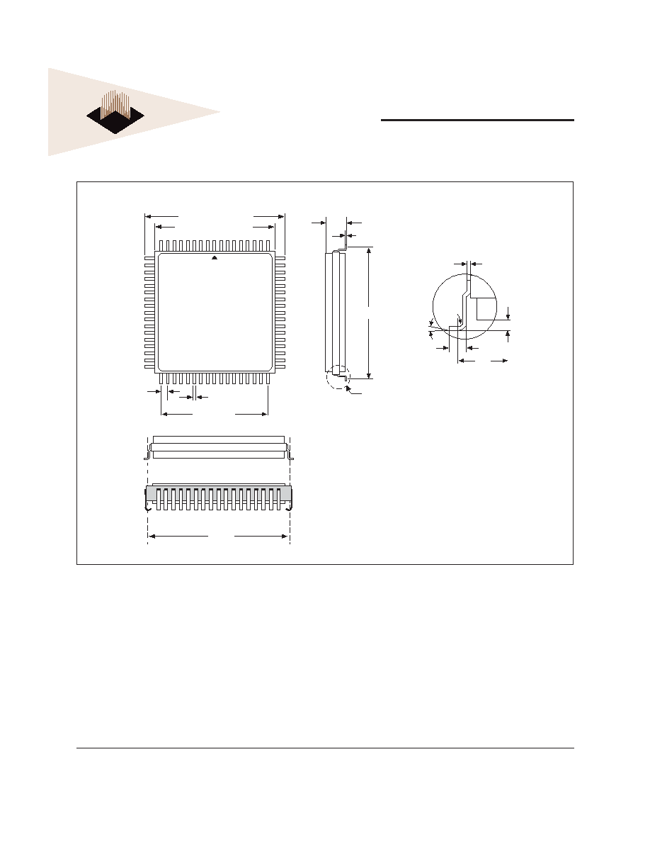
PACKAGE 509: 68 LEAD, CERAMIC QUAD FLAT PACK, CQFP (G2T)
ALL LINEAR DIMENSIONS ARE MILLIMETERS AND PARENTHETICALLY IN INCHES
0.38 (0.015) ± 0.05 (0.002)
0.27 (0.011) ± 0.04 (0.002)
25.15 (0.990) ± 0.26 (0.010) SQ
1.27 (0.050) TYP
24.03 (0.946)
± 0.26 (0.010)
22.36 (0.880) ± 0.26 (0.010) SQ
20.3 (0.800) REF
4.57 (0.180) MAX
0.19 (0.007)
± 0.06 (0.002)
23.87
(0.940) REF
1.0 (0.040)
± 0.127 (0.005)
0.25 (0.010) REF
1
∞ / 7∞
R 0.25
(0.010)
DETAIL A
SEE DETAIL "A"
Pin 1
The WEDC 68 lead G2T
CQFP fi lls the same fi t and
function as the JEDEC 68
lead CQFJ or 68 PLCC.
But the G2T has the TCE
and lead inspection advan-
tage of the CQFP form.
0.940"

14
White Electronic Designs Corporation ∑ (602) 437-1520 ∑ www.wedc.com
White Electronic Designs
WSF512K32-XXX
May 2006
Rev. 9
LEAD
FINISH:
Blank = Gold plated leads
A = Solder dip leads
DEVICE
GRADE:
M = Military Screened
-55∞C to +125∞C
I
=
Industrial
-40∞C
to
+85∞C
C = Commercial
0∞C to +70∞C
PACKAGE
TYPE:
H2 = Ceramic Hex In-line Package, HIP (Package 402)
G2T = 22.4mm Ceramic Quad Flat Pack, CQFP (Package 509)
ACCESS
TIME
(ns)
29 = 25ns SRAM and 90ns FLASH
ORGANIZATION, 512K x 32 SRAM and Flash
Flash
SRAM
WHITE
ELECTRONIC
DESIGNS
CORP.
ORDERING INFORMATION
W S F 512K32 - 29 X X X
PACKAGE 402: 66 PIN, PGA TYPE, CERAMIC HEX-IN-LINE PACKAGE, HIP (H2)
35.2 (1.385) ± 0.38 (0.015) SQ
25.4 (1.0) TYP
15.24 (0.600) TYP
0.76 (0.030) ± 0.1 (0.005)
5.7 (0.223)
MAX
3.81 (0.150)
± 0.1 (0.005)
2.54 (0.100)
TYP
25.4 (1.0) TYP
1.27 (0.050) ± 0.1 (0.005)
1.27 (0.050) TYP DIA
0.46 (0.018) ± 0.05 (0.002) DIA
PIN 1 IDENTIFIER
SQUARE PAD
ON BOTTOM
ALL LINEAR DIMENSIONS ARE MILLIMETERS AND PARENTHETICALLY IN INCHES