1
White Electronic Designs Corporation ∑ (602) 437-1520 ∑ www.wedc.com
White Electronic Designs
April 2005
Rev. 0
ADVANCED*
White Electronic Designs Corp. reserves the right to change products or specifi cations without notice.
WV3EG6434S-BD4
256MB ≠ 32Mx64 DDR SDRAM UNBUFFERED, w/PLL
DESCRIPTION
The WV3EG6434S is a 32Mx64 Double Data Rate
SDRAM memory module based on 256Mb DDR
SDRAM component. The module consists of eight
32Mx8 DDR SDRAMs in BGA package mounted on a
200 Pin FR4 substrate.
Synchronous design allows precise cycle control with
the use of system clock. Data I/O transactions are
possible on both edges and Burst Lenths allow the
same device to be useful for a variety of high bandwidth,
high performance memory system applications.
* This product is under development, is not qualifi ed or characterized and is subject to
change or cancellation without notice.
FEATURES
DDR266 and DDR333
Double-data-rate
architecture
Bi-directional data strobes (DQS)
Differential clock inputs (CK & CK#)
Programmable Read Latency 2,2.5 (clock)
Programmable
Burst
Length
(2,4,8)
Programmable Burst type (sequential & interleave)
Edge aligned data output, center aligned data input
Auto and self refresh
Serial presence detect
Power supply: 2.5V ± 0.20V
Standard 200 pin SO-DIMM package
∑ Package height options:
BD4: 31.75mm (1.25")
NOTE: Consult factory for availability of:
∑ Lead-Free or RoHS Products
∑ Vendor source control options
∑ Industrial temperature option
OPERATING FREQUENCIES
DDR333 @CL=2.5
DDR266 @CL=2
DDR266 @CL=2.5
Clock Speed
166MHz
133MHz
133MHz
CL-t
RCD
-t
RP
2.5-3-3
2-2-2
2.5-3-3
2
White Electronic Designs Corporation ∑ (602) 437-1520 ∑ www.wedc.com
White Electronic Designs
WV3EG6434S-BD4
April 2005
Rev. 0
ADVANCED
White Electronic Designs Corp. reserves the right to change products or specifi cations without notice.
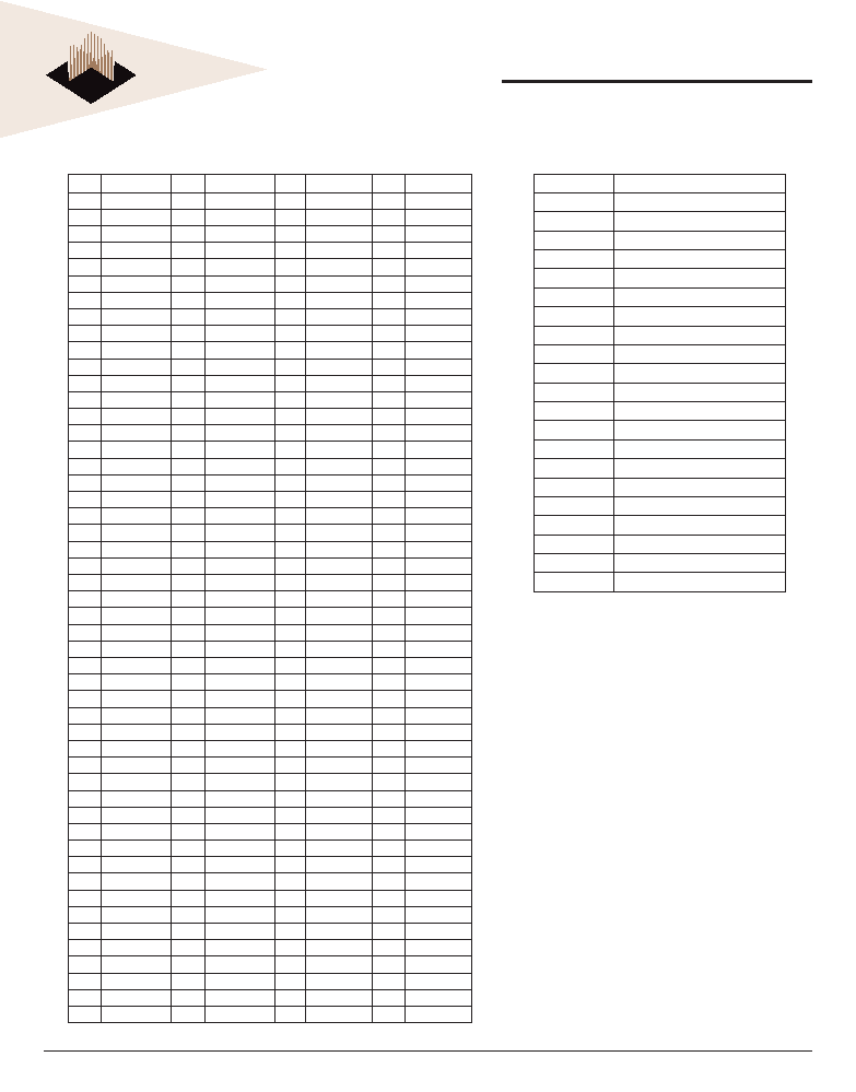
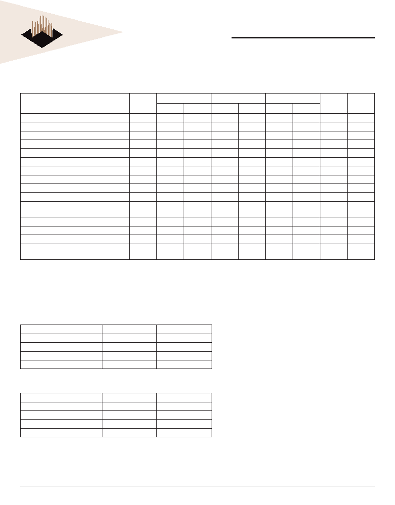
PIN NAMES
A0 ≠ A12
Address input (Multiplexed)
BA0-BA1
Bank Select Address
DQ0-DQ63
Data Input/Output
DQS0-DQS7
Data Strobe Input/Output
CK0
Clock input
CK0#
Clock input
CKE0 Clock
Enable
Input
CS0#
Chip select Input
RAS#
Row Address Strobe
CAS#
Column Address Strobe
WE#
Write Enable
DM0-DM7
Data-In Mask
V
CC
Power Supply
V
CCQ
Power Supply for DQS
V
SS
Ground
V
REF
Power Supply for Reference
V
CCSPD
Serial EEPROM Power Supply
SDA
Serial data I/O
SCL
Serial clock
SA0-SA2
Address in EEPROM
V
CCID
V
CC
Identifi cation Flag
NC
No Connect
* These pins are not used in this module.
PIN CONFIGURATIONS
Pin
Symbol
Pin
Symbol
Pin
Symbol
Pin
Symbol
1
V
REF
51
V
SS
101
A9
151
DQ42
2
V
REF
52
V
SS
102
A8
152
DQ46
3
V
SS
53
DQ19
103
V
SS
153
DQ43
4
V
SS
54
DQ23
104
V
SS
154
DQ47
5
DQ0
55
DQ24
105
A7
155
V
CC
6
DQ4
56
DQ28
106
A6
156
V
CC
7
DQ1
57
V
CC
107
A5
157
V
CC
8
DQ5
58
V
CC
108
A4
158
*CK1#
9
V
CC
59
DQ25
109
A3
159
V
SS
10
V
CC
60
DQ29
110
A2
160
*CK1
11
DQS0
61
DQS3
111
A1
161
V
SS
12
DM0
62
DM3
112
A0
162
V
SS
13
DQ2
63
V
SS
113
V
CC
163
DQ48
14
DQ6
64
V
SS
114
V
CC
164
DQ52
15
V
SS
65
DQ26
115
A10/AP
165
DQ49
16
V
SS
66
DQ30
116
BA1
166
DQ53
17
DQ3
67
DQ27
117
BA0
167
V
CC
18
DQ7
68
DQ31
118
RAS#
168
V
CC
19
DQ8
69
V
CC
119
WE#
169
DQS6
20
DQ12
70
V
CC
120
CAS#
170
DM6
21
V
CC
71
NC
121
CS0
171
DQ50
22
V
CC
72
NC
122
*CS1#
172
DQ54
23
DQ9
73
NC
123
NC
173
V
SS
24
DQ13
74
NC
124
NC
174
V
SS
25
DQS1
75
V
SS
125
V
SS
175
DQ51
26
DM1
76
V
SS
126
V
SS
176
DQ55
27
V
SS
77
*DQS8
127
DQ32
177
DQ56
28
V
SS
78
*DM8
128
DQ36
178
DQ60
29
DQ10
79
NC
129
DQ33
179
V
CC
30
DQ14
80
NC
130
DQ37
180
V
CC
31
DQ11
81
V
CC
131
V
CC
181
DQ57
32
DQ15
82
V
CC
132
V
CC
182
DQ61
33
V
CC
83
NC
133
DQS4
183
DQS7
34
V
CC
84
NC
134
DM4
184
DM7
35
CK0
85
NC
135
DQ34
185
V
SS
36
V
CC
86
NC
136
DQ38
186
V
SS
37
CK0#
87
V
SS
137
V
SS
187
DQ58
38
V
SS
88
V
SS
138
V
SS
188
DQ62
39
V
SS
89
*CK2
139
DQ35
189
DQ59
40
V
SS
90
V
SS
140
DQ39
190
DQ63
41
DQ16
91
*CK2#
141
DQ40
191
V
CC
42
DQ20
92
V
CC
142
DQ44
192
V
CC
43
DQ17
93
V
CC
143
V
CC
193
SDA
44
DQ21
94
V
CC
144
V
CC
194
SA0
45
V
CC
95
*CKE1
145
DQ41
195
SCL
46
V
CC
96
CKE0
146
DQ45
196
SA1
47
DQS2
97
NC
147
DQS5
197
V
CCSPD
48
DM2
98
NC
148
DM5
198
SA2
49
DQ18
99
A12
149
V
SS
199
NC
50
DQ22
100
A11
150
V
SS
200
NC
3
White Electronic Designs Corporation ∑ (602) 437-1520 ∑ www.wedc.com
White Electronic Designs
WV3EG6434S-BD4
April 2005
Rev. 0
ADVANCED
White Electronic Designs Corp. reserves the right to change products or specifi cations without notice.
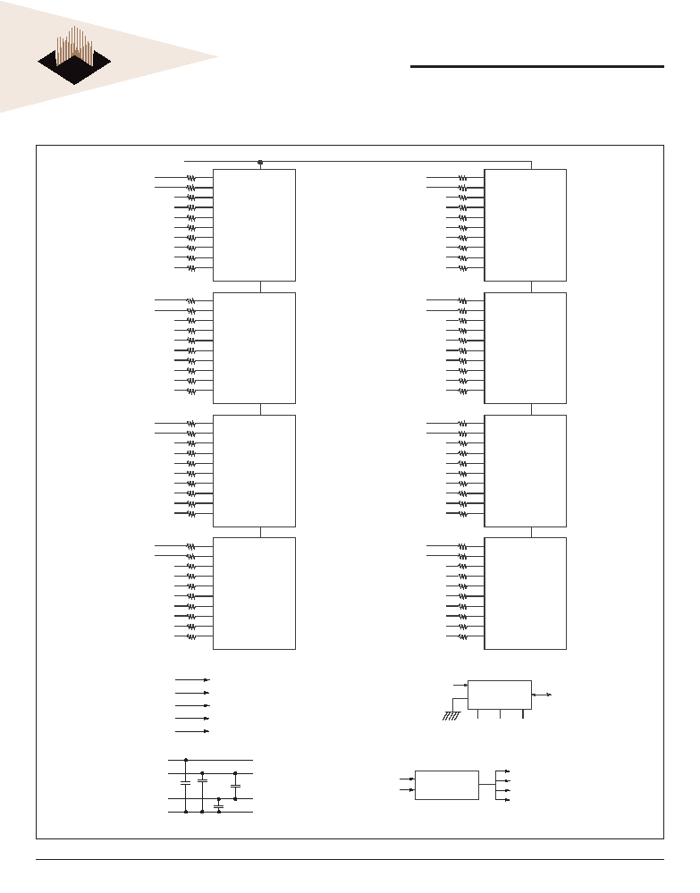
FUNCTIONAL BLOCK DIAGRAM
CKE0
I/0 0
I/0 1
I/0 2
I/0 3
I/0 4
I/0 5
I/0 6
I/0 7
DQ0
DQ1
DQ2
DQ3
DQ4
DQ5
DQ6
DQ7
DQS
S0#
A0 - A12
A0-A12: DDR SDRAMs
BA0 - BA1
BA0-BA1: DDR SDRAMs
RAS#
RAS#: SDRAMs
CAS#
CAS#: SDRAMs
WE#
WE#: SDRAMs
A0
Serial PD
A1
A2
SA0
SA1
SA2
SCL
SDA
WP
DM
DQS0
DM0
I/0 0
I/0 1
I/0 2
I/0 3
I/0 4
I/0 5
I/0 6
I/0 7
DQS
S0#
DM
DQS4
DM4
I/0 0
I/0 1
I/0 2
I/0 3
I/0 4
I/0 5
I/0 6
I/0 7
DQ8
DQ9
DQ10
DQ11
DQ12
DQ13
DQ14
DQ15
DQS
S1#
DM
DQS1
DM1
I/0 0
I/0 1
I/0 2
I/0 3
I/0 4
I/0 5
I/0 6
I/0 7
DQS
S1#
DM
DQS5
DM5
I/0 0
I/0 1
I/0 2
I/0 3
I/0 4
I/0 5
I/0 6
I/0 7
DQ16
DQ17
DQ18
DQ19
DQ20
DQ21
DQ22
DQ23
DQS
S0#
DM
DQS2
DM2
I/0 0
I/0 1
I/0 2
I/0 3
I/0 4
I/0 5
I/0 6
I/0 7
DQS
S0#
DM
DQS6
DM6
I/0 0
I/0 1
I/0 2
I/0 3
I/0 4
I/0 5
I/0 6
I/0 7
DQ24
DQ25
DQ26
DQ27
DQ28
DQ29
DQ30
DQ31
DQS
S1#
DM
DQS3
DM3
I/0 0
I/0 1
I/0 2
I/0 3
I/0 4
I/0 5
I/0 6
I/0 7
DQS
S1#
DM
DQS7
DM7
DQ32
DQ33
DQ34
DQ35
DQ36
DQ37
DQ38
DQ39
DQ40
DQ41
DQ42
DQ43
DQ44
DQ45
DQ46
DQ47
DQ48
DQ49
DQ50
DQ51
DQ52
DQ53
DQ54
DQ55
DQ56
DQ57
DQ58
DQ59
DQ60
DQ61
DQ62
DQ63
S0#
PLL
CK0
DDR SDRAM
CK0#
DDR SDRAM
DDR SDRAM
DDR SDRAM
V
SS
DDR SDRAM
DDR SDRAM
DDR SDRAM
V
REF
V
CCSPD
V
CC
/V
CCQ
SPD
NOTE: All resistor values are 22 ohms unless otherwise specifi ed.
4
White Electronic Designs Corporation ∑ (602) 437-1520 ∑ www.wedc.com
White Electronic Designs
WV3EG6434S-BD4
April 2005
Rev. 0
ADVANCED
White Electronic Designs Corp. reserves the right to change products or specifi cations without notice.
ABSOLUTE MAXIMUM RATINGS
Parameter
Symbol
Value
Units
Voltage on any pin relative to V
SS
V
IN
, V
OUT
-0.5 to 3.6
V
Voltage on V
CC
supply relative to V
SS
V
CC
, V
CCQ
-1.0 to 3.6
V
Storage Temperature
T
STG
-55 to +150
∞C
Power Dissipation
P
D
8
W
Short Circuit Current
I
OS
50
mA
Note:
Permanent device damage may occur if "ABSOLUTE MAXIMUM RATINGS" are exceeded.
Functional operation should be restricted to recommended operating condition.
Exposure to higher than recommended voltage for extended periods of time could affect device reliability.
DC OPERATING CONDITIONS
T
A
= 0∞C to 70∞C
Parameter
Symbol
Min
Max
Unit
Note
Supply voltage(for device with a nominal V
CC
of 2.5V)
V
CC
2.3
2.7
V
I/O Supply voltage
V
CCQ
2.3
2.7
V
I/O Reference voltage
V
REF
V
CCQ
/2-50mV
V
CCQ
/2+50mV
V
1
I/O Termination voltage (system)
V
TT
V
REF
-0.04
V
REF
+0.04
V
2
Input logic high voltage
V
IH
(DC)
V
REF
+0.15
V
CCQ
+0.3
V
4
Input logic low voltage
V
IL
(DC)
-0.3
V
REF
-0.15
V
4
Input Voltage Level, CK and CK# inputs
V
IN
(DC)
-0.3
V
CCQ
+0.3
V
Input Differential Voltage, CK and CK# inputs
V
ID
(DC)
0.3
V
CCQ
+0.6
V
3
Input crossing point voltage, CK and CK# inputs
V
IX
(DC)
1.15
1.35
V
5
Input leakage current
I
I
-2
2
uA
Output leakage current
I
OZ
-5
5
uA
Output High Current(Normal strengh driver); V
OUT
= V
TT
+ 0.84V
I
OH
-16.8
mA
Output High Current(Normal strengh driver); V
OUT
= V
TT
- 0.84V
I
OL
16.8
mA
Output High Current(Half strengh driver); V
OUT
= V
TT
+ 0.45V
I
OH
-9
mA
Output High Current(Half strengh driver); V
OUT
= V
TT
- 0.45V
I
OL
9
mA
Notes:
1.
Includes ± 25mV margin for DC offset on V
REF
, and a combined total of ± 50mV margin for all AC noise and DC offset on V
REF
, bandwidth limited to 20MHz. The DRAM must
accommodate DRAM current spikes on V
REF
and internal DRAM noise coupled TO V
REF
, both of which may result in V
REF
noise. V
REF
should be de-coupled with an inductance of 3nH.
2. V
TT
is not applied directly to the device. V
TT
is a system supply for signal termination resistors, is expected to be set equal to V
REF
, and must track variations in the DC level of V
REF
3. V
ID
is the magnitude of the difference between the input level on CK and the input level on CK.
4.
These parameters should be tested at the pin on actual components and may be checked at either the pin or the pad in simulation. The AC and DC input specifi cations are relative to a
V
REF
envelop that has been bandwidth limited to 200MHZ.
5.
The value of V
IX
is expected to equal 0.5*V
CCQ
of the transmitting device and must track variations in the dc level of the same.
CAPACITANCE
T
A
= 25∞C, f = 1MHz, V
CC
= 2.5V, V
REF
=2.5V ± 200mV
Parameter
Symbol
Max
Unit
Input Capacitance (A0-A12)
C
IN1
21
pF
Input Capacitance (RAS#, CAS#, WE#)
C
IN2
21
pF
Input Capacitance (CKE0)
C
IN3
21
pF
Input Capacitance (CK0,CK0#)
C
IN4
3
pF
Input Capacitance (CS0#)
C
IN5
12
pF
Input Capacitance (DQM0-DQM8)
C
IN6
10
pF
Input Capacitance (BA0-BA1)
C
IN7
21
pF
Data input/output capacitance (DQ0-DQ63)(DQS)
C
OUT
10
pF

5
White Electronic Designs Corporation ∑ (602) 437-1520 ∑ www.wedc.com
White Electronic Designs
WV3EG6434S-BD4
April 2005
Rev. 0
ADVANCED
White Electronic Designs Corp. reserves the right to change products or specifi cations without notice.
I
DD
SPECIFICATIONS AND TEST CONDITIONS
Recommended operating conditions, 0∞C T
A
70∞C, V
CCQ
= 2.5V ±0.2V, V
CC
= 2.5V ±0.2V
DDR333@
CL=2.5
DDR266@
CL=2
DDR266@
CL=2.5
Parameter
Symbol Conditions
Max
Max
Max
Units
Operating Current
I
DD0
One device bank; Active - Precharge; t
RC
=t
RC
(MIN); t
CK
=t
CK
(MIN);
DQ,DM and DQS inputs changing once per clock cycle; Address
and control inputs changing once every two cycles.
720
640
640
mA
Operating Current
I
DD1
One device bank; Active-Read-Precharge; Burst = 2; t
RC
=t
RC
(MIN
);t
CK
=t
CK
(MIN); Iout = 0mA; Address and control inputs changing
once per clock cycle.
920
840
840
mA
Precharge Power-Down
Standby Current
I
DD2P
All device banks idle; Power- down mode; t
CK
=t
CK
(MIN);
CKE=(low)
24
24
24
mA
Idle Standby Current
I
DD2F
CS# = High; All device banks idle; t
CK
=t
CK
(MIN); CKE = high;
Address and other control inputs changing once per clock cycle.
Vin = Vref for DQ, DQS and DM.
240
200
200
mA
Precharge Quiet
Standby Current
I
DD2Q
CS# > = V
IH
(min); All banks idle; CKE > = V
IH
(min); t
CK
= 100Mhz
for DDR200, 133Mhz for DDR266A & DDR266B; Address and
other control inputs stable with keeping >= V
IH
(min) or =
< V
IL
(max); V
IN
= V
REF
for DQ, DQS and DM
200
185
185
mA
Active Power-Down
Standby Current
I
DD3P
One device bank active; Power-down mode; t
CK
(MIN); CKE=(low)
280
240
240
mA
Active Standby Current
I
DD3N
CS# = High; CKE = High; One device bank; Active-Precharge;
t
RC
=t
RAS
(MAX); t
CK
=t
CK
(MIN); DQ, DM and DQS inputs changing
twice per clock cycle; Address and other control inputs changing
once per clock cycle.
440
360
360
mA
Operating Current
I
DD4R
Burst = 2; Reads; Continous burst; One device bank
active;Address and control inputs changing once per clock cycle;
t
CK
=t
CK
(MIN); Iout = 0mA.
1280
1120
1120
mA
Operating Current
I
DD4W
Burst = 2; Writes; Continous burst; One device bank active;
Address and control inputs changing once per clock cycle;
t
CK
=t
CK
(MIN); DQ,DM and DQS inputs changing twice per clock
cycle.
1280
1080
1080
mA
Auto Refresh Current
I
DD5
t
RC
=t
RC
(MIN)
1360
1280
1280
mA
Self Refresh Current
I
DD6
CKE
0.2V
24
24
24
mA
Operating Current
I
DD7A
Four bank interleaving Reads (BL=4) with auto precharge with
t
RC
=t
RC
(MIN); t
CK
=t
CK
(MIN); Address and control inputs change
only during Active Read or Write commands.
2240
2080
2080
mA
Note: I
DD
speicifi cation is based on Samsung components. Other DRAM manufacturers specifi cation may be different.

6
White Electronic Designs Corporation ∑ (602) 437-1520 ∑ www.wedc.com
White Electronic Designs
WV3EG6434S-BD4
April 2005
Rev. 0
ADVANCED
White Electronic Designs Corp. reserves the right to change products or specifi cations without notice.
I
DD1
: OPERATING CURRENT : ONE BANK
1. Typical
Case
:
V
CC
=2.5V, T=25∞C
2. Worst
Case
:
V
CC
=2.7V, T=10∞C
3. Only one bank is accessed with t
RC
(min), Burst
Mode, Address and Control inputs on NOP edge
are changing once per clock cycle. I
OUT
= 0mA
4. Timing
Patterns
:
∑
DDR200 (100 MHz, CL=2) : t
CK=
10ns, CL2,
BL=4, t
RCD=
2*t
CK
, t
RAS=
5*t
CK
Read : A0 N R0 N N P0 N A0 N - repeat the
same timing with random address changing;
50% of data changing at every burst
∑
DDR266 (133MHz, CL=2.5) : t
CK=
7.5ns,
CL=2.5, BL=4, t
RCD=
3*t
CK
, t
RC=
9*t
CK
, t
RAS=
5*t
CK
Read : A0 N N R0 N P0 N N N A0 N - repeat
the same timing with random address
changing; 50% of data changing at every burst
∑
DDR266 (133MHz, CL=2) : t
CK
=7.5ns, CL=2,
BL=4, t
RCD
=3*t
CK
, t
RC
=9*t
CK
, t
RAS
=5*t
CK
Read : A0 N N R0 N P0 N N N A0 N - repeat
the same timing with random address
changing; 50% of data changing at every burst
∑
DDR333 (166MHz, CL=2.5) : t
CK
=6ns, BL=4,
t
RCD
=10*t
CK
, t
RAS
=7*t
CK
Read : A0 N N R0 N P0 N N N A0 N - repeat
the same timing with random address
changing; 50% of data changing at every burst
I
DD7A
: OPERATING CURRENT : FOUR BANKS
1. Typical
Case
:
V
CC
=2.5V, T=25∞C
2. Worst
Case
:
V
CC
=2.7V, T=10∞C
3. Four banks are being interleaved with t
RC
(min),
Burst Mode, Address and Control inputs on NOP
edge are not changing. Iout=0mA
4. Timing
Patterns
:
∑
DDR200 (100 MHz, CL=2) : t
CK
=10ns, CL2,
BL=4, t
RRD
=2*t
CK
, t
RCD
=3*t
CK
, Read with
Autoprecharge
Read : A0 N A1 R0 A2 R1 A3 R2 A0 R3 A1 R0
- repeat the same timing with random address
changing; 100% of data changing at every
burst
∑
DDR266 (133MHz, CL=2.5) : t
CK
=7.5ns,
CL=2.5, BL=4, t
RRD
=3*t
CK
, t
RCD
=3*t
CK
Read with Autoprecharge
Read : A0 N A1 R0 A2 R1 A3 R2 N R3 A0 N
A1 R0 - repeat the same timing with random
address changing; 100% of data changing at
every burst
∑
DDR266 (133MHz, CL=2) : t
CK
=7.5ns, CL2=2,
BL=4, t
RRD
=2*t
CK
, t
RCD
=2*t
CK
Read : A0 N A1 R0 A2 R1 A3 R2 N R3 A0 N
A1 R0 - repeat the same timing with random
address changing; 100% of data changing at
every burst
∑
DDR333 (166MHz, CL=2.5) : t
CK
=6ns,
BL=4, t
RRD
=3*t
CK
, t
RCD
=3*t
CK
, Read with
Autoprecharge
Read : A0 N A1 R0 A2 R1 A3 R2 N R3 A0 N
A1 R0 - repeat the same timing with random
address changing; 100% of data changing at
every burst
DETAILED TEST CONDITIONS FOR DDR SDRAM I
DD1
& I
DD7A
Legend : A = Activate, R = Read, W = Write, P = Precharge, N = NOP
A (0-3) = Activate Bank 0-3
R (0-3) = Read Bank 0-3

7
White Electronic Designs Corporation ∑ (602) 437-1520 ∑ www.wedc.com
White Electronic Designs
WV3EG6434S-BD4
April 2005
Rev. 0
ADVANCED
White Electronic Designs Corp. reserves the right to change products or specifi cations without notice.
DDR SDRAM COMPONENT ELECTRICAL CHARACTERISTICS AND RECOMMENDED AC
OPERATING CONDITIONS
0∞C T
A
70∞C, V
CC
= +2.5V ±0.2V, V
CCQ
= +2.5V ±0.2V
Parameter
Symbol
335
262
265
Unit
Note
Min
Max
Min
Max
Min
Max
Row cycle time
t
RC
60
65
65
ns
Refresh row cycle time
t
RFC
72
75
75
ns
Row active time
t
RAS
42
70K
45
120K
45
120K
ns
RAS to CAS delay
t
RCD
18
20
20
ns
Row precharge time
t
RP
18
20
20
ns
Row active to Row active delay
t
RRD
12
15
15
ns
Write recovery time
t
WR
15
15
15
ns
Last data in to Read command
t
WTR
1
1
1
t
CK
Col. address to Col. address delay
t
CCD
1
1
1
t
CK
Clock cycle time
CL=2.0
t
CK
7.5
12
7.5
12
10
12
ns
5
CL=2.5
6
12
7.5
12
7.5
12
ns
5
Clock high level width
t
CH
0.45
0.55
0.45
0.55
0.45
0.55
t
CK
Clock low level width
t
CL
0.45
0.55
0.45
0.55
0.45
0.55
t
CK
DQS-out access time from CK/CK#
t
DQSCK
-0.6
+0.6
-0.75
+0.75
-0.75
+0.75
ns
Output data access time from CK/CK#
t
AC
-0.7
+0.7
-0.75
+0.75
-0.75
+0.75
ns
Data strobe edge to ouput data edge
t
DQSQ
-
0.45
-
0.5
-
0.5
ns
5
Read Preamble
t
RPRE
0.9
1.1
0.9
1.1
0.9
1.1
t
CK
Read Postamble
t
RPST
0.4
0.6
0.4
0.6
0.4
0.6
t
CK
CK to valid DQS-in
t
DQSS
0.75
1.25
0.75
1.25
0.75
1.25
t
CK
DQS-in setup time
t
WPRES
0
0
0
ns
2
DQS-in hold time
t
WPRE
0.25
0.25
0.25
t
CK
DQS falling edge to CK rising-setup time
t
DSS
0.2
0.2
0.2
t
CK
DQS falling edge from CK rising-hold time
t
DSH
0.2
0.2
0.2
t
CK
DQS-in high level width
t
DQSH
0.35
0.35
0.35
t
CK
DQS-in low level width
t
DQSL
0.35
0.35
0.35
t
CK
DQS-in cycle time
t
DSC
0.9
1.1
0.9
1.1
0.9
1.1
t
CK
Address and Control Input setup time (fast)
t
IS
0.75
0.9
0.9
ns
6
Address and Control Input hold time (fast)
t
IH
0.75
0.9
0.9
ns
6
Address and Control Input setup time (slow)
t
IS
0.8
1.0
1.0
ns
6
Address and Control Input hold time (slow)
t
IH
0.8
1.0
1.0
ns
6
Data-out high impedence time from CK/CK#
t
HZ
-0.7
+0.7
-0.75
+0.75
-0.75
+0.75
ns
Data-out low impedence time from CK/CK#
t
LZ
-0.7
+0.7
-0.75
+0.75
-0.75
+0.75
ns
Input Slew Rate (for input only pins)
t
SL(I)
0.5
0.5
0.5
V/ns
6
Input Slew Rate (for I/O pins)
t
SL(IO)
0.5
0.5
0.5
V/ns
7
Output Slew Rate (x4,x8)
t
SL(O)
1.0
4.5
1.0
4.5
1.0
4.5
V/ns
Output Slew Rate Matching Ratio (rise to fall)
t
SLMR
0.67
1.5
0.67
1.5
0.67
1.5
Note: AC Timing Parameters are based on Samsung components. Other DRAM Manufacturers parameters may be different.
8
White Electronic Designs Corporation ∑ (602) 437-1520 ∑ www.wedc.com
White Electronic Designs
WV3EG6434S-BD4
April 2005
Rev. 0
ADVANCED
White Electronic Designs Corp. reserves the right to change products or specifi cations without notice.
DDR SDRAM COMPONENT ELECTRICAL CHARACTERISTICS AND RECOMMENDED AC
OPERATING CONDITIONS (Continued)
0∞C T
A
70∞C, V
CC
= +2.5V ±0.2V, V
CCQ
= +2.5V ±0.2V
Parameter
Symbol
335
262
265
Unit
Note
Min
Max
Min
Max
Min
Max
Mode register set cycle time
t
MRD
12
15
15
ns
DQ & DM setup time to DQS
t
DS
0.45
0.5
0.5
ns
7
DQ & DM hold time to DQS
t
DH
0.45
0.5
0.5
ns
7
Control & Address input pulse width
t
IPW
2.2
2.2
2.2
ns
DQ & DM input pulse width
t
DIPW
1.75
1.75
1.75
ns
Power down exit time
t
PDEX
6
7.5
7.5
ns
Exit self refresh to non-Read command
t
XSNR
75
75
75
ns
4
Exit self refresh to read command
t
XSRD
200
200
200
t
CK
Refresh interval time
t
REFI
7.8
7.8
7.8
us
1
Output DQS valid window
t
QH
t
HP
-t
QHS
--
t
HP
-t
QHS
--
t
HP
-t
QHS
--
ns
5
Clock half period
t
HP
t
CLmin
or
t
CHmin
--
t
CLmin
or
t
CHmin
--
t
CLmin
or
t
CHmin
--
ns
Data hold skew factor
t
QHS
0.55
0.75
0.75
ns
DQS write postamble time
t
WPST
0.4
0.6
0.4
0.6
0.4
0.6
t
CK
3
Active to Read with Auto precharge command
t
RAP
18
20
20
Autoprecharge write recovery + Precharge
time
t
DAL
(t
WR
/t
CK
) +
(t
RP
/t
CK
)
(t
WR
/t
CK
) +
(t
RP
/t
CK
)
(t
WR
/t
CK
) +
(t
RP
/t
CK
)
t
CK
1.
Maximum burst refresh cycle : 8
2.
The specifi c requirement is that DQS be valid(High or Low) on or before this CK edge. The case shown(DQS going from High_Z to logic Low) applies when no writes were
previously in progress on the bus. If a previous write was in progress, DQS could be High at this time, depending on tDQSS.
3.
The maximum limit for this parameter is not a device limit. The device will operate with a great value for this parameter, but system performance (bus turnaround) will degrade
accordingly.
4.
A write command can be applied with tRCD satisfi ed after this command.
5.
For registered DIMMs, tCL and tCH are >_ 45% of the period including both the half period jitter (tJIT(HP)) of the PLL and the half period jitter due to crosstalk (tJIT(crosstalk)) on
the DIMM.
6.
Input Setup/Hold Slew Rate Derating
Input Setup/Hold Slew Rate
t
IS
t
IH
(V/ns)
(ps)
(ps)
0.5
0
0
0.4
+50
+50
0.3
+100
+100
This derating table is used to increase t
IS
/t
IH
in the case where the input slew rate is below 0.5V/ns. Input setup/hold slew rate based on the lesser of AC-AC slew rate
and DC-DC slew rate.
7.
I/O Setup/Hold Slew Rate Derating
I/O Setup/Hold Slew Rate
t
DS
t
DH
(V/ns)
(ps)
(ps)
0.5
0
0
0.4
+75
+75
0.3
+150
+150
This derating table is used to increase t
DS
/t
DH
in the case where the I/O slew rate is below 0.5V/ns. I/O setup/hold slew rate based on the lesser of AC-AC slew rate
and DC-DC slew rate.
9
White Electronic Designs Corporation ∑ (602) 437-1520 ∑ www.wedc.com
White Electronic Designs
WV3EG6434S-BD4
April 2005
Rev. 0
ADVANCED
White Electronic Designs Corp. reserves the right to change products or specifi cations without notice.
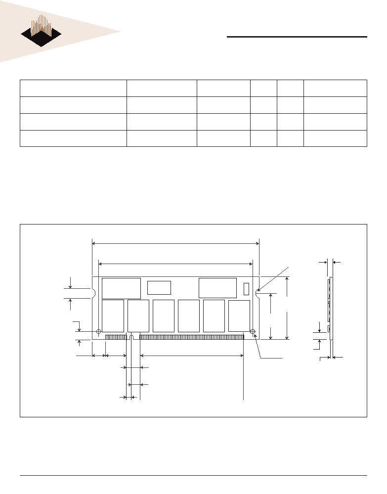
PACKAGE DIMENSIONS FOR BD4
1.0 ± 0.1
(0.039 ± 0.004)
2.54
(0 .100)
MAX.
3.98
(0.157)
MIN.
Full R 2X
1
39
41
199
4.00 ±0.10
(0.16 ±0.039)
6.00
(0.24)
2.15
(0.086)
11.40
(0.456)
1.80
(0.07)
2.40
(0.096)
4.20
(0.17)
47.40
(1.896)
2- 1.80
(0.07)
31.75
(1.25)
20.00
(0.79)
63.60
(2.50)
67.56
(2.66)
ORDERING INFORMATION FOR BD4
Part Number
Speed
CAS Latency
t
RCD
t
RP
Height*
WV3EG6434S335BD4
166MHz/333Mb/s
2.5
3
3
31.75 (1.25")
WV3EG6434S262BD4
133MHz/266Mb/s
2
2
2
31.75 (1.25")
WV3EG6434S265BD4
133MHz/266Mb/s
2.5
3
3
31.75 (1.25")
NOTES:
∑ Consult Factory for availability of Lead-Free or RoHS products. (F = Lead-Free, G = RoHS Compliant)
∑ Vendor specifi c part numbers are used to provide memory components source control. The place holder for this is shown as lower case "x" in the part numbers above and is to
be replaced with the respective vendors code. Consult factory for qualifi ed sourcing options. (M = Micron, S = Samsung & consult factory for others)
∑ Consult factory for availability of industrial temperature (-40∞C to 85∞C) option
* ALL DIMENSIONS ARE IN MILLIMETERS AND (INCHES)
TOLERANCES: ± 0.15 (0.006) UNLESS OTHERWISE SPECIFIED

10
White Electronic Designs Corporation ∑ (602) 437-1520 ∑ www.wedc.com
White Electronic Designs
WV3EG6434S-BD4
April 2005
Rev. 0
ADVANCED
White Electronic Designs Corp. reserves the right to change products or specifi cations without notice.
Document Title
256MB ≠ 32Mx64 DDR SDRAM UNBUFFERED, w/PLL
Revision History
Rev #
History
Release Date
Status
Rev 0
Created
4-05
Advanced