1
White Electronic Designs Corporation ∑ (602) 437-1520 ∑ www.wedc.com
White Electronic Designs
ADVANCED*
White Electronic Designs Corp. reserves the right to change products or specifi cations without notice.
June 2006
Rev. 0
WV3EG6437S-D4
256MB ≠ 2x16Mx64 DDR SDRAM SO-DIMM, UNBUFFERED
DESCRIPTION
The WV3EG6437S is a 2x16Mx64 Double Data Rate
SDRAM memory module based on 256Mb DDR SDRAM
components. The module consists of eight 16Mx16 DDR
SDRAMs in 66 pin TSOP package mounted on a 200 Pin
FR4 substrate.
* This product is under development, is not qualifi ed or characterized and is subject to
change without notice.
FEATURES
Unbuffered Double-data-rate architecture
DDR300 and DDR400
∑ JEDEC design specifi cations
Bi-directional data strobes (DQS)
Differential clock inputs (CK & CK#)
Programmable Read Latency 2.5, 3
Programmable Burst Length (2,4,8)
Programmable Burst type (sequential & interleave)
Edge aligned data output, center aligned data input
Auto and self refresh, (8K/64ms Refresh)
Serial presence detect with EEPROM
Dual
Rank
Power Supply: V
CC
= V
CC
: 2.5V ± 0.2V (DDR300)
V
CC
= V
CCQ
: 2.6V ± 0.1V (DDR400)
JEDEC standard 200 pin SO-DIMM package
∑ Package height options:
D4: 31.75mm (1.25") TYP
NOTE: Consult factory for availability of:
∑ RoHS compliant products
∑ Vendor source control options
∑ Industrial temperature option
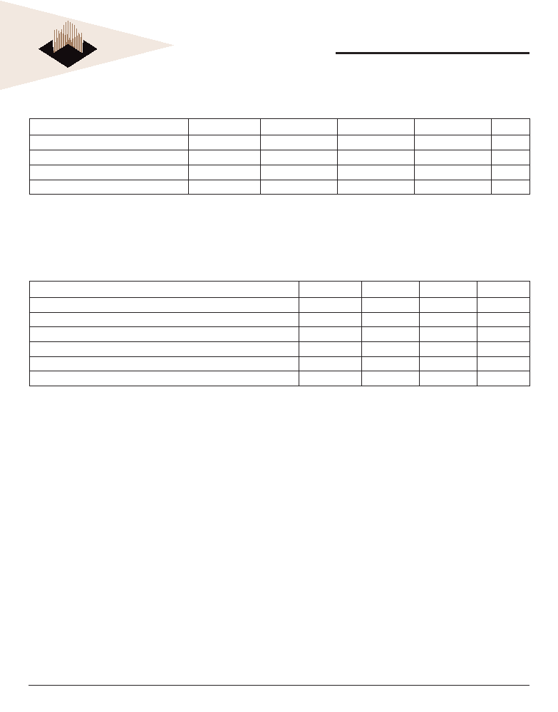
OPERATING FREQUENCIES
DDR400@CL=3
DDR333@CL=2.5
Clock Speed
200MHz
166MHz
CL-t
RCD
-t
RP
3-3-3
2.5-3-3
2
White Electronic Designs Corporation ∑ (602) 437-1520 ∑ www.wedc.com
White Electronic Designs
June 2006
Rev. 0
White Electronic Designs Corp. reserves the right to change products or specifi cations without notice.
ADVANCED
WV3EG6437S-D4
PIN NAMES
A0 ≠ A12
Address input
BA0-BA1
Bank Select Address
DQ0-DQ63
Data Input/Output
DQS0-DQS7
Data Strobe Input/Output
CK0, CK1
Clock Inputs
CK0#, CK1#
CKE0, CKE1
Clock Enable Inputs
CS0#, CS1#
Chip select Inputs
RAS#
Row Address Strobe
CAS#
Column Address Strobe
WE#
Write Enable
DM0-DM7
Data Mask
V
CC
Power Supply
V
SS
Ground
V
REF
Reference Power Supply
V
CCSPD
Serial EEPROM Power Supply
SDA
Serial data I/O
SCL
SPD clock input
SA0-SA2
SPD address
NC
No Connect
PIN CONFIGURATIONS
Pin
Symbol
Pin
Symbol
Pin
Symbol
Pin
Symbol
1
V
REF
51
V
SS
101
A9
151
DQ42
2
V
REF
52
V
SS
102
A8
152
DQ46
3
V
SS
53
DQ19
103
V
SS
153
DQ43
4
V
SS
54
DQ23
104
V
SS
154
DQ47
5
DQ0
55
DQ24
105
A7
155
V
CC
6
DQ4
56
DQ28
106
A6
156
V
CC
7
DQ1
57
V
CC
107
A5
157
V
CC
8
DQ5
58
V
CC
108
A4
158
CK1#
9
V
CC
59
DQ25
109
A3
159
V
SS
10
V
CC
60
DQ29
110
A2
160
CK1
11
DQS0
61
DQS3
111
A1
161
V
SS
12
DM0
62
DM3
112
A0
162
V
SS
13
DQ2
63
V
SS
113
V
CC
163
DQ48
14
DQ6
64
V
SS
114
V
CC
164
DQ52
15
V
SS
65
DQ26
115
A10
165
DQ49
16
V
SS
66
DQ30
116
BA1
166
DQ53
17
DQ3
67
DQ27
117
BA0
167
V
CC
18
DQ7
68
DQ31
118
RAS#
168
V
CC
19
DQ8
69
V
CC
119
WE#
169
DQS6
20
DQ12
70
V
CC
120
CAS#
170
DM6
21
V
CC
71
NC
121
CS0#
171
DQ50
22
V
CC
72
NC
122
CS1#
172
DQ54
23
DQ9
73
NC
123
NC
173
V
SS
24
DQ13
74
NC
124
NC
174
V
SS
25
DQS1
75
V
SS
125
V
SS
175
DQ51
26
DM1
76
V
SS
126
V
SS
176
DQ55
27
V
SS
77
NC
127
DQ32
177
DQ56
28
V
SS
78
NC
128
DQ36
178
DQ60
29
DQ10
79
NC
129
DQ33
179
V
CC
30
DQ14
80
NC
130
DQ37
180
V
CC
31
DQ11
81
V
CC
131
V
CC
181
DQ57
32
DQ15
82
V
CC
132
V
CC
182
DQ61
33
V
CC
83
NC
133
DQS4
183
DQS7
34
V
CC
84
NC
134
DM4
184
DM7
35
CK0
85
NC
135
DQ34
185
V
SS
36
V
CC
86
NC
136
DQ38
186
V
SS
37
CK0#
87
V
SS
137
V
SS
187
DQ58
38
V
SS
88
V
SS
138
V
SS
188
DQ62
39
V
SS
89
NC
139
DQ35
189
DQ59
40
V
SS
90
V
SS
140
DQ39
190
DQ63
41
DQ16
91
NC
141
DQ40
191
V
CC
42
DQ20
92
V
CC
142
DQ44
192
V
CC
43
DQ17
93
V
CC
143
V
CC
193
SDA
44
DQ21
94
V
CC
144
V
CC
194
SA0
45
V
CC
95
CKE1
145
DQ41
195
SCL
46
V
CC
96
CKE0
146
DQ45
196
SA1
47
DQS2
97
NC
147
DQS5
197
V
CCSPD
48
DM2
98
NC
148
DM5
198
SA2
49
DQ18
99
A12
149
V
SS
199
NC
50
DQ22
100
A11
150
V
SS
200
NC
3
White Electronic Designs Corporation ∑ (602) 437-1520 ∑ www.wedc.com
White Electronic Designs
June 2006
Rev. 0
White Electronic Designs Corp. reserves the right to change products or specifi cations without notice.
ADVANCED
WV3EG6437S-D4
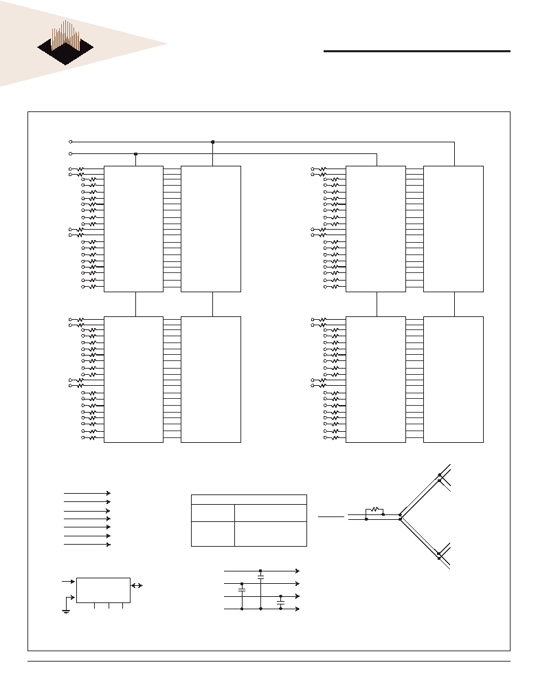
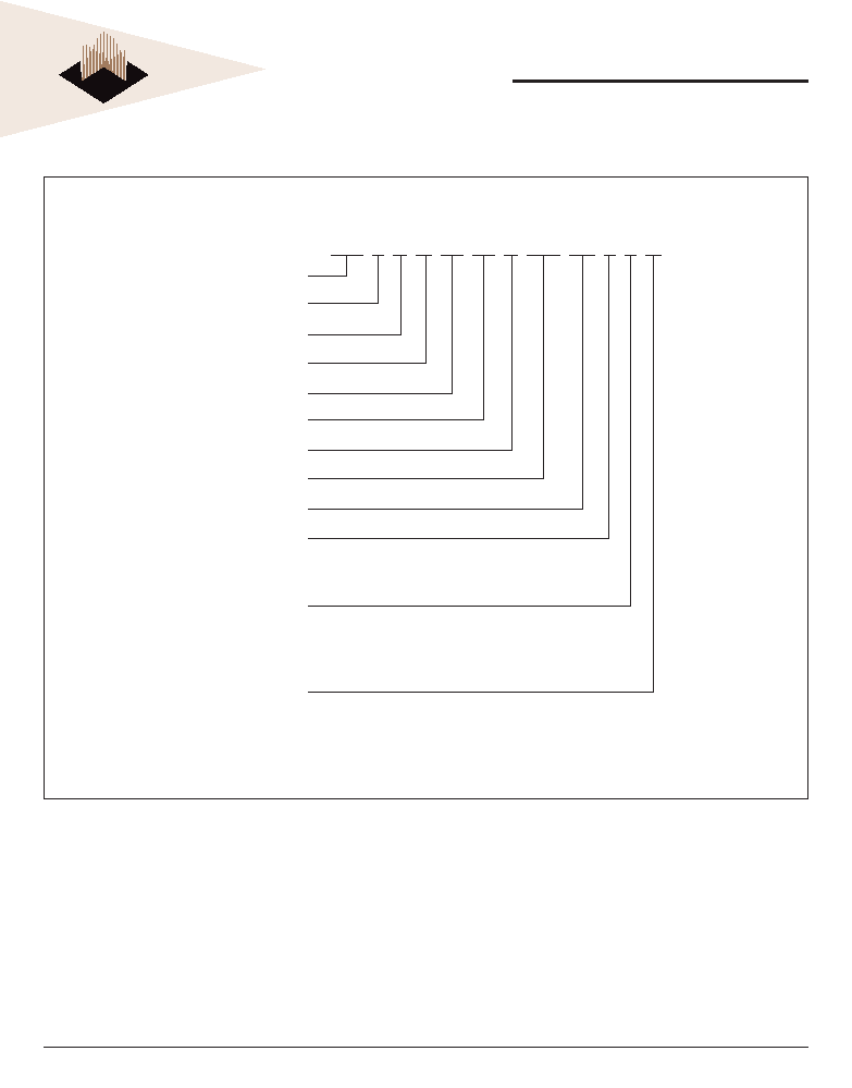
FUNCTIONAL BLOCK DIAGRAM
CS1#
CS0#
DQS0
DM0
DQS1
DM1
DQ0
DQ1
DQ2
DQ3
DQ4
DQ5
DQ6
DQ7
DQ8
DQ9
DQ10
DQ11
DQ12
DQ13
DQ14
DQ15
DQS2
DM2
DQS3
DM3
DQ16
DQ17
DQ18
DQ19
DQ20
DQ21
DQ22
DQ23
DQ24
DQ25
DQ26
DQ27
DQ28
DQ29
DQ30
DQ31
LDQS
LDM
DQ0
DQ1
DQ2
DQ3
DQ4
DQ5
DQ6
DQ7
UDQS
UDQM
DQ8
DQ9
DQ10
DQ11
DQ12
DQ13
DQ14
DQ15
CS#
LDQS
LDM
DQ0
DQ1
DQ2
DQ3
DQ4
DQ5
DQ6
DQ7
UDQS
UDQM
DQ8
DQ9
DQ10
DQ11
DQ12
DQ13
DQ14
DQ15
CS#
LDQS
LDM
DQ0
DQ1
DQ2
DQ3
DQ4
DQ5
DQ6
DQ7
UDQS
UDQM
DQ8
DQ9
DQ10
DQ11
DQ12
DQ13
DQ14
DQ15
CS#
LDQS
LDM
DQ0
DQ1
DQ2
DQ3
DQ4
DQ5
DQ6
DQ7
UDQS
UDQM
DQ8
DQ9
DQ10
DQ11
DQ12
DQ13
DQ14
DQ15
CS#
DQS4
DM4
DQS5
DM5
DQ32
DQ33
DQ34
DQ35
DQ36
DQ37
DQ38
DQ39
DQ40
DQ41
DQ42
DQ43
DQ44
DQ45
DQ46
DQ47
DQS6
DM6
DQS7
DM7
DQ48
DQ49
DQ50
DQ51
DQ52
DQ53
DQ54
DQ55
DQ56
DQ57
DQ58
DQ59
DQ60
DQ61
DQ62
DQ63
LDQS
LDM
DQ0
DQ1
DQ2
DQ3
DQ4
DQ5
DQ6
DQ7
UDQS
UDQM
DQ8
DQ9
DQ10
DQ11
DQ12
DQ13
DQ14
DQ15
CS#
LDQS
LDM
DQ0
DQ1
DQ2
DQ3
DQ4
DQ5
DQ6
DQ7
UDQS
UDQM
DQ8
DQ9
DQ10
DQ11
DQ12
DQ13
DQ14
DQ15
CS#
LDQS
LDM
DQ0
DQ1
DQ2
DQ3
DQ4
DQ5
DQ6
DQ7
UDQS
UDQM
DQ8
DQ9
DQ10
DQ11
DQ12
DQ13
DQ14
DQ15
CS#
LDQS
LDM
DQ0
DQ1
DQ2
DQ3
DQ4
DQ5
DQ6
DQ7
UDQS
UDQM
DQ8
DQ9
DQ10
DQ11
DQ12
DQ13
DQ14
DQ15
CS#
A0
SA0
SERIAL PD
SDA
A1
SA1
A2
SA2
BA0, BA1
A0-A12
RAS#
BA0, BA1: DDR SDRAMs
A0-A12: DDR SDRAMs
RAS#: DDR SDRAMs
CAS#: DDR SDRAMs
CKE0: DDR SDRAMs
WE#: DDR SDRAMs
CAS#
CKE0
WE#
V
REF
V
SS
DDR SDRAMs
DDR SDRAMs
CKE1: DDR SDRAMs
CKE1
WP
SCL
V
CCSPD
V
CC
DDR SDRAMs
DDR SDRAMs
DDR SDRAMs
DDR SDRAMs
Clock Wiring
Clock
Input
CK0/CK0#
CK1/CK1#
4 SDRAMs
4 SDRAMs
SPD
DDR SDRAMs
CK0/1
CK0/1#
R=120
Note: All resistor values are 22 ohms ±5% unless otherwise specifi ed.
4
White Electronic Designs Corporation ∑ (602) 437-1520 ∑ www.wedc.com
White Electronic Designs
June 2006
Rev. 0
White Electronic Designs Corp. reserves the right to change products or specifi cations without notice.
ADVANCED
WV3EG6437S-D4
ABSOLUTE MAXIMUM RATINGS
Parameter
Symbol
Value
Units
Voltage on any pin relative to V
SS
V
IN
, V
OUT
-0.5 to 3.6
V
Voltage on V
CC
supply relative to V
SS
V
CC
, V
CCQ
-0.5 to 3.6
V
Storage Temperature
T
STG
-55 to +150
∞C
Operating Temperature
T
A
0 - 70
∞C
Power Dissipation
P
D
8
W
Short Circuit Current
I
OS
50
mA
Note:
Permanent device damage may occur if "ABSOLUTE MAXIMUM RATINGS" are exceeded.
Functional operation should be restricted to recommended operating condition.
Exposure to higher than recommended voltage for extended periods of time could affect device reliability.
DC CHARACTERISTICS
0∞C T
A
70∞C
Parameter
Symbol
Min
Max
Unit
Supply voltage DDR333
V
CC
2.3
2.7
V
I/O Supply voltage DDR333
V
CCQ
2.3
2.7
V
Supply Voltage DDR400
V
CC
2.5
2.7
V
I/O Supply Voltage DDR400
V
CCQ
2.5
2.7
V
I/O Reference voltage
V
REF
0.49 + V
CC
0.51 + V
CC
V
I/O Termination voltage
V
TT
V
REF
- 0.04
V
REF
+ 0.04
V
Input logic high voltage
V
IH(DC)
V
REF
+ 0.15
V
CC
+ 0.30
V
Input logic low voltage
V
IL(DC)
-0.3
V
REF
- 0.15
V
Input voltage level, CK and CK#
V
In(DC)
-0.3
V
CC
+ 0.30
V
Input differential voltage, CK and CK#
V
ID(DC)
0.36
V
CC
+ 0.60
V
Input crossing point voltage, CK and CK#
V
IX(DC)
0.3
V
CC
+ 0.60
V
Input leakage current
Addr, CAS#, RAS#, WE#
I
I
-16
16
µA
CS#, CKE
-8
8
µA
CK, CK#
-8
8
µA
DM
-4
4
µA
Output leackage current
DQ, DQS
I
OZ
-10
10
µA
Output high surrent (normal strength)
V
OUT
= V
TT
+ 0.84V
I
OH
-16.8
-
mA
Output high surrent (normal strength)
V
OUT
= V
TT
- 0.84V
I
OL
16.8
-
mA
Output high surrent (half strength)
V
OUT
= V
TT
+ 0.45V
I
OH
-9
-
mA
Output high surrent (half strength)
V
OUT
= V
TT
- 0.45V
I
OL
9
-
mA
Notes:
1. V
REF
is expected to equal 0.5*V
CCQ
of the transmitting device and to track variations in the DC level of the same. Peak-to-peak noise on V
REF
may not exceed +/-2 percent of the
DC value.
2. V
TT
in sot applied directly to the device. V
TT
is a system supply for signal termination resistors, is expected to be set equal to V
REF
and must track variations in the DC level of V
REF
.
3. V
ID
is the magnitude of the difference between the input level on CK and the input level of CK#.
4. V
CCQ
of all IC's are ited to V
CC
.
5
White Electronic Designs Corporation ∑ (602) 437-1520 ∑ www.wedc.com
White Electronic Designs
June 2006
Rev. 0
White Electronic Designs Corp. reserves the right to change products or specifi cations without notice.
ADVANCED
WV3EG6437S-D4
AC OPERATING CONDITIONS
All voltages referenced to V
SS
Parameter
Symbol
Min.
Max.
Units
Notes
Input High (Logic1) Voltage
V
IH(AC)
V
REF
+ 0.31
V
1
Input Low (Logic0) Voltage
V
IL(AC)
V
REF
- 0.31
V
1
Input Differential Voltage, CK and CK# input
V
ID(AC)
0.7
V
CCQ
+ 0.6
V
Input Crossing Point Voltage, CK and CK# input
V
IX(AC)
0.5*V
CC
- 0.2
0.5*V
CC
+ 0.2
V
Notes:
1. V
IH
overshoot: V
IN
= V
CC
+ 1.5V for a pulse width 3ns and the pulse can not be greater than 1/3 of the cycle rate.
V
IL
undershoot: V
IL
= -1.5V for a pulse width 3ns and the pulse can not be greater than 1/3 of the cycle rate.
INPUT/OUTPUT CAPACITANCE
T
A
= 25∞C, f = 100MHz
Parameter
Symbol
Min
Max
Units
Input Capacitance (A0~A12, BA0~BA1, RAS#, CAS#, WE#)
C
IN1
20
28
pF
Input Capacitance (CKE0, CKE1)
C
IN2
12
16
pF
Input Capacitance (CS0#, CS1#)
C
IN3
12
16
pF
Input Capacitance CK, CK0#, CK1, CK1#)
C
IN4
12
16
pF
Input Capacitance (DM0 ~ DM7), (DQS0 ~ DQS7)
C
IN5
12
14
pF
Input Capacitance (DQ0 ~ DQ63)
C
OUT1
12
14
pF
6
White Electronic Designs Corporation ∑ (602) 437-1520 ∑ www.wedc.com
White Electronic Designs
June 2006
Rev. 0
White Electronic Designs Corp. reserves the right to change products or specifi cations without notice.
ADVANCED
WV3EG6437S-D4
I
CC
SPECIFICATIONS AND TEST CONDITIONS
Parameter
Symbol Conditions
DDR403
@CL=3
Max
DDR333
@CL=2.5
Max
Units
Operating Current
I
CC0*
One device bank; Active - Precharge; t
RC
=t
RC
(MIN); t
CK
=t
CK
(MIN); DQ,DM
and DQS inputs changing once per clock cycle; Address and control inputs
changing once every two cycles.
456
372
mA
Operating Current
I
CC1*
One device bank; Active-Read-Precharge; Burst = 2; t
RC
=t
RC
(MIN);t
CK
=t
CK
(MIN)
; Iout = 0mA; Address and control inputs changing once per clock cycle.
616
512
mA
Precharge Power-
Down Standby Current
I
CC2P**
All device banks idle; Power- down mode; t
CK
=t
CK
(MIN); CKE=(low)
32
24
mA
Idle Standby Current
I
CC2F**
CS# = High; All device banks idle; t
CK
=t
CK
(MIN); CKE = high; Address and other
control inputs changing once per clock cycle. Vin = Vref for DQ, DQS and DM.
240
240
mA
Active Power-Down
Standby Current
I
CC3P**
One device bank active; Power-down mode; t
CK
(MIN); CKE=(low)
400
280
mA
Active Standby Current
I
CC3N**
CS# = High; CKE = High; One device bank; Active-Precharge; t
RC
=t
RAS
(MAX);
t
CK
=t
CK
(MIN); DQ, DM and DQS inputs changing twice per clock cycle; Address
and other control inputs changing once per clock cycle.
520
440
mA
Operating Current
I
CC4R*
Burst = 2; Reads; Continous burst; One device bank active;Address and control
inputs changing once per clock cycle; t
CK
=t
CK
(MIN); Iout = 0mA.
736
652
mA
Operating Current
I
CC4W**
Burst = 2; Writes; Continous burst; One device bank active; Address and
control inputs changing once per clock cycle; t
CK
=t
CK
(MIN); DQ,DM and DQS
inputs changing twice per clock cycle.
736
652
mA
Auto Refresh Current
I
CC5**
t
RC
=t
RC
(MIN)
1,600
1,440
mA
Self Refresh Current
I
CC6**
CKE 0.2V
24
24
mA
Operating Current
I
CC7*
Four bank interleaving Reads (BL=4) with auto precharge with t
RC
=t
RC
(MIN);
t
CK
=t
CK
(MIN); Address and control inputs change only during Active Read or
Write commands.
1,416
1,332
mA
Note: I
CC
specifi cation is based on
SAMSUNG components. Other DRAM Manufacturers specifi cation may be different.
* Value calculated as one module rank in this operation condition, and all other module ranks in I
CC2P
(CKE LOW) mode.
** Value calculated refl ects all module ranks in the operating condition.

7
White Electronic Designs Corporation ∑ (602) 437-1520 ∑ www.wedc.com
White Electronic Designs
June 2006
Rev. 0
White Electronic Designs Corp. reserves the right to change products or specifi cations without notice.
ADVANCED
WV3EG6437S-D4
DDR SDRAM COMPONENT ELECTRICAL CHARACTERISTICS AND
RECOMMENDED AC OPERATING CONDITIONS
AC CHARACTERISTICS
403
335
UNITS
PARAMETER
SYMBOL
MIN
MAX
MIN
MAX
Access window of DQs from CK/CK#
t
AC
-0.65
+0.65
-0.7
+0.7
ns
CK high-level width
t
CH
0.45
0.55
0.45
0.55
t
CK
CK low-level width
t
CL
0.45
0.55
0.45
0.55
t
CK
Clock cycle time
CL = 3
t
CK (3)
5
10
ns
CL = 2.5
t
CK (2.5)
6
12
ns
DQ and DM input hold time relative to DQS
t
DH
0.40
0.40
ns
DQ and DM input setup time relative to DQS
t
DS
0.40
0.40
ns
DQ and DM input pulse width (for each input)
t
DIPW
1.75
1.75
ns
Access window of DQS from CK/CK#
t
DQSCK
-0.55
+0.65
-0.60
+0.60
ns
DQS input high pulse width
t
DQSH
0.35
0.35
t
CK
DQS input low pulse width
t
DQSL
0.35
0.35
t
CK
DQS-DQ skew, DQS to last DQ valid, per group, per access
t
DQSQ
0.40
0.45
ns
Write command to fi rst DQS latching transition
t
DQSS
0.72
1.28
0.75
1.25
t
CK
DQS falling edge to CK rising - setup time
t
DSS
0.20
0.20
t
CK
DQS falling edge from CK rising - hold time
t
DSH
0.20
0.20
t
CK
Half clock period
t
HP
t
CH(MIN)
or
t
CL(MIN)
t
CH(MIN)
or
(MIN)
ns
Data-out high-impedance window from CK/CK#
t
HZ
+0.65
+0.70
ns
Data-out low-impedance window from CK/CK#
t
LZ
-0.65
-0.70
ns
Address and control input hold time (1 V/ns)
t
IHF
0.60
0.75
ns
Address and control input setup time (1 V/ns)
t
ISF
0.60
0.75
ns
Address and control input hold time (0.5 V/ns)
t
IHS
0.70
0.80
ns
Address and control input setup time (0.5 V/ns)
t
ISS
0.70
0.75
ns
Address and Control input pulse width (for each input)
t
IPW
2.20
2.20
ns
LOAD MODE REGISTER command cycle time
t
MRD
10
10
ns
DQ-DQS hold, DQS to fi rst DQ to go non-valid, per access
t
QH
t
HP
- t
QHS
t
HP
- t
QHS
ns
Data hold skew factor
t
QHS
0.50
0.55
ns
ACTIVE to PRECHARGE command
t
RAS
40
70K
42
70K
ns
ACTIVE to READ with Auto precharge command
t
RAP
15
18
ns
ACTIVE to ACTIVE/AUTO REFRESH command period
t
RC
55
60
ns
AUTO REFRESH command period
t
RFC
70
72
ns
ACTIVE to READ or WRITE delay
t
RCD
15
18
ns
PRECHARGE command period
t
RP
15
18
ns
DQS read preamble
t
RPRE
0.90
1.10
0.9
1.10
t
CK
DQS read postamble
t
RPST
0.40
0.60
0.4
0.60
t
CK
ACTIVE bank a to ACTIVE bank b command
t
RRD
10
12
ns
DQS write preamble
t
WPRE
0.25
0.25
t
CK
DQS write preamble setup time
t
WPRES
0
0
ns
Note: AC specifi cation is based on
SAMSUNG components. Other DRAM manufactures specifi cation may be different.
Continued on next page
8
White Electronic Designs Corporation ∑ (602) 437-1520 ∑ www.wedc.com
White Electronic Designs
June 2006
Rev. 0
White Electronic Designs Corp. reserves the right to change products or specifi cations without notice.
ADVANCED
WV3EG6437S-D4
DDR SDRAM COMPONENT ELECTRICAL CHARACTERISTICS AND
RECOMMENDED AC OPERATING CONDITIONS (Continued)
AC CHARACTERISTICS
403
355
PARAMETER
SYMBOL
MIN
MAX
MIN
MAX
UNITS
DQS write postamble
t
WPST
0.40
0.60
0.40
0.60
t
CK
Write recovery time
t
WR
15
15
ns
Internal WRITE to READ command delay
t
WTR
2
1
t
CK
Average periodic refresh interval
t
REFI
7.80
7.80
µs
Exit SELF REFRESH to non-READ command
t
XSNR
75
75
ns
Exit SELF REFRESH to READ command
t
XSRD
200
200
t
CK
Auto precharge write recovery + precharge time
t
RAL
t
WR
/t
CK
+
t
RP
/t
CK
t
WR
/t
CK
+
t
RP
/t
CK
t
CK
Note: AC specifi cation is based on
SAMSUNG components. Other DRAM manufactures specifi cation may be different.
9
White Electronic Designs Corporation ∑ (602) 437-1520 ∑ www.wedc.com
White Electronic Designs
June 2006
Rev. 0
White Electronic Designs Corp. reserves the right to change products or specifi cations without notice.
ADVANCED
WV3EG6437S-D4
* ALL DIMENSIONS ARE IN MILLIMETERS AND (INCHES)
PACKAGE DIMENSIONS FOR D4
3.81 (0.150)
MAX
1.10 (0.043)
0.90 (0.035)
PIN 1
67.75 (2.667)
67.45 (2.656)
20.00 (0.787)
TYP
1.80 (0.071)
(2X)
0.60 (0.024)
TYP
0.45 (0.018)
TYP
(2X)
PIN 199
PIN 200
PIN 2
FRONT VIEW
2.15 (0.085)
6.00 (0.240)
2.504 (63.60)
2.55 (0.100)
1.00 (0.039)
TYP
TYP
BACK VIEW
31.90 (1.256)
31.60 (1.244)
47.40 (1.866)
TYP
11.40 (0.449)
TYP
4.2 (0.165)
TYP
3.90(0.154)
4.10(0.161)
4.06 (0.160)
1.80 (0.071)
1.50 (0.059)
ORDERING INFORMATION FOR D4
Part Number
Speed/Data Rate Frequency
Height*
WV3EG6437S403D4xxG
200MHz/400Mbps, CL=3
31.75 (1.25") TYP
WV3EG6437S335D4xxG
166MHz/333Mbps, CL=2.5
31.75 (1.25") TYP
NOTES:
∑ Consult Factory for availability of RoHS compliant products. (G = RoHS Compliant)
∑
Vendor
specifi c part numbers are used to provide memory components source control. The place holder for this is shown as lower case "x" in the part numbers above and is to
be replaced with the respective vendors code. Consult factory for qualifi ed sourcing options. (M = Micron, S = Samsung & consult factory for others)
∑ Consult factory for availability of industrial temperature (-40∞C to 85∞C) option
10
White Electronic Designs Corporation ∑ (602) 437-1520 ∑ www.wedc.com
White Electronic Designs
June 2006
Rev. 0
White Electronic Designs Corp. reserves the right to change products or specifi cations without notice.
ADVANCED
WV3EG6437S-D4
PART NUMBERING GUIDE
WV 3 E G 64 37 S xxx D4 x x G
WEDC
MEMORY
DDR
GOLD
BUS WIDTH
2x16M
2.5V
SPEED (Mb/s)
PACKAGE 200 PIN
INDUSTRIAL TEMP OPTION
(For commercial leave "blank"
for industrial add "I"
COMPONENT VENDOR NAME
(M = Micron)
(S = Samsung)
(N = Nanya)
G = RoHS COMPLIANT

11
White Electronic Designs Corporation ∑ (602) 437-1520 ∑ www.wedc.com
White Electronic Designs
June 2006
Rev. 0
White Electronic Designs Corp. reserves the right to change products or specifi cations without notice.
ADVANCED
WV3EG6437S-D4
Document Title
256MB ≠ 32Mx64, DDR SDRAM UNBUFFERED
DRAM DIE OPTIONS:
∑
SAMSUNG: H-Die (K4H561638H-UCB3) RoHS
∑
MICRON: T26A: F-Die
Revision History
Rev #
History
Release Date Status
Rev 0
Created
June 2006
Advanced