WV3HG2128M72AER-D6
September
2005 Rev. 0
ADVANCED*
1
White Electronic Designs Corporation ∑ (602) 437-1520 ∑ www.wedc.com
White Electronic Designs
2GB ≠ 2x128Mx72 DDR2 SDRAM REGISTERED, w/PLL
DESCRIPTION
The WV3HG2128M72AER is a 128Mx72 Double Data
Rate DDR2 SDRAM high density module. This memory
module consists of thirty six 128Mx4 bit with 4 banks DDR2
Synchronous DRAMs in FBGA packages, mounted on a
240-pin DIMM FR4 substrate.
* This product is under development, is not qualifi ed or characterized and is subject to
change or cancellation without notice.
NOTE: Consult factory for availability of:
∑ Vendor source control options
∑ Industrial temperature option
FEATURES
240-pin, dual in-line memory module
Fast data transfer rates: PC2-4200 and PC2-3200
Utilizes 533 and 400 Mb/s DDR2 SDRAM
components
V
CC
= V
CCQ
= 1.8V
±
0.1V
V
CCSPD
= 1.7V to 3.6V
JEDEC standard 1.8V I/O (SSTL_18-compatible)
Differential data strobe (DQS, DQS#) option
Four-bit
prefetch
architecture
DLL to align DQ and DQS transitions with CK
Multiple internal device banks for concurrent
operation
Supports duplicate output strobe (RDQS/RDQS#)
Programmable CAS# latency (CL): 3 and 4
Adjustable data-output drive strength
On-die
termination
(ODT)
Serial Presence Detect (SPD) with EEPROM
64ms: 8,192 cycle refresh
Gold edge contacts
Product
is
lead-free
RoHS
compliant
Dual
Rank
Package
option
∑ 240 Pin DIMM
∑ PCB ≠ 29.97mm (1.18")
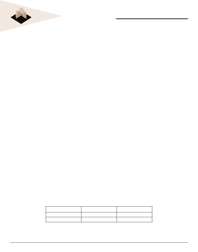
OPERATING FREQUENCIES
PC2-3200
PC2-4200
Clock Speed
200MHz
266MHz
CL-t
RCD
-t
RP
3-3-3
4-4-4

WV3HG2128M72AER-D6
ADVANCED*
2
White Electronic Designs Corporation ∑ (602) 437-1520 ∑ www.wedc.com
White Electronic Designs
September
2005 Rev. 0
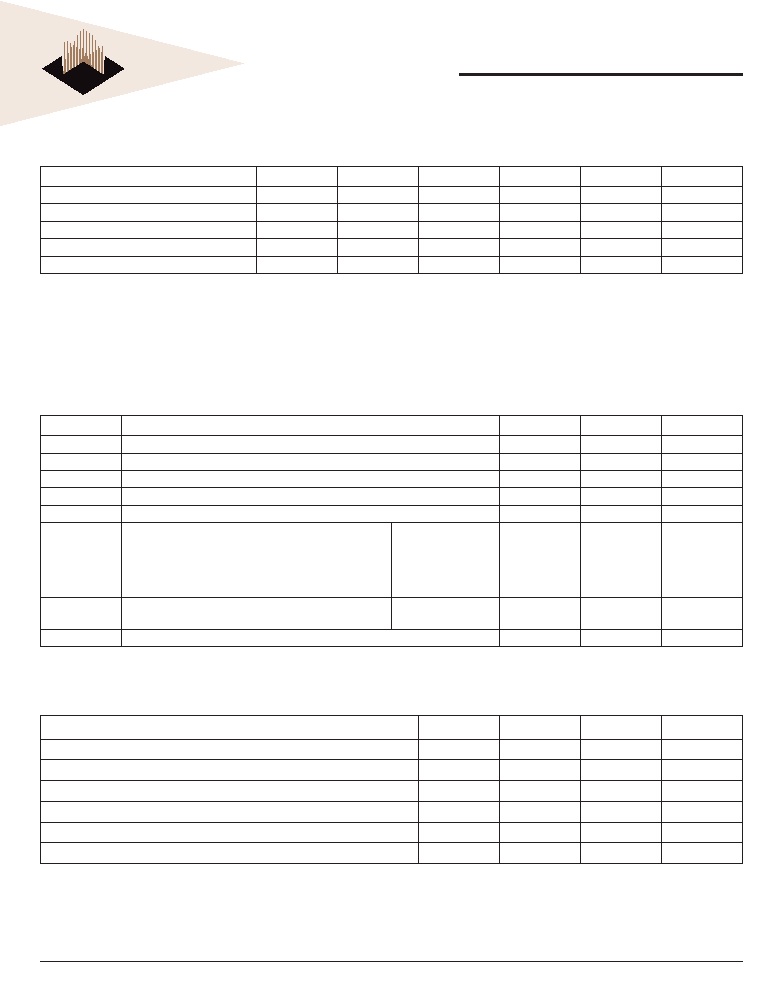
PIN CONFIGURATION
Pin No.
Symbol
Pin No.
Symbol
Pin No.
Symbol
Pin No.
Symbol
1
V
REF
61
A4
121
V
SS
181
V
CCQ
2
V
SS
62
V
CCQ
122
DQ4
182
A3
3
DQ0
63
A2
123
DQ5
183
A1
4
DQ1
64
V
CC
124
V
SS
184
V
CC
5
V
SS
65
V
SS
125
DQS9
185
CK0
6
DQS0#
66
V
SS
126
DQS9#
186
CK0#
7
DQS0
67
V
CC
127
V
SS
187
V
CC
8
V
SS
68
NC
128
DQ6
188
A0
9
DQ2
69
V
CC
129
DQ7
189
V
CC
10
DQ3
70
A10/AP
130
V
SS
190
BA1
11
V
SS
71
BA0
131
DQ12
191
V
CCQ
12
DQ8
72
V
CCQ
132
DQ13
192
RAS#
13
DQ9
73
WE#
133
V
SS
193
S0#
14
V
SS
74
CAS#
134
DQS10
194
V
CCQ
15
DQS1#
75
V
CCQ
135
DQS10#
195
ODT0
16
DQS1
76
CS1#
136
V
SS
196
A13
17
V
SS
77
ODT1
137
NC
197
V
CC
18
RESET#
78
V
CCQ
138
NC
198
V
SS
19
NC
79
V
SS
139
V
SS
199
DQ36
20
V
SS
80
DQ32
140
DQ14
200
DQ37
21
DQ10
81
DQ33
141
DQ15
201
V
SS
22
DQ11
82
V
SS
142
V
SS
202
DQS13
23
V
SS
83
DQS4#
143
DQ20
203
DQS13#
24
DQ16
84
DQS4
144
DQ21
204
V
SS
25
DQ17
85
V
SS
145
V
SS
205
DQ38
26
V
SS
86
DQ34
146
DQS11
206
DQ39
27
DQS2#
87
DQ35
147
DQS11#
207
V
SS
28
DQS2
88
V
SS
148
V
SS
208
DQ44
29
V
SS
89
DQ40
149
DQ22
209
DQ45
30
DQ18
90
DQ41
150
DQ23
210
V
SS
31
DQ19
91
V
SS
151
V
SS
211
DQS14
32
V
SS
92
DQS5#
152
DQ28
212
DQS14#
33
DQ24
93
DQS5
153
DQ29
213
V
SS
34
DQ25
94
V
SS
154
V
SS
214
DQ46
35
V
SS
95
DQ42
155
DQS12
215
DQ47
36
DQS3#
96
DQ43
156
DQS12#
216
V
SS
37
DQS3
97
V
SS
157
V
SS
217
DQ52
38
V
SS
98
DQ48
158
DQ30
218
DQ53
39
DQ26
99
DQ49
159
DQ31
219
V
SS
40
DQ27
100
V
SS
160
V
SS
220
NC
41
V
SS
101
SA2
161
CB4
221
NC
42
CB0
102
NC
162
CB5
222
V
SS
43
CB1
103
V
SS
163
V
SS
223
DQS15
44
V
SS
104
DQS6#
164
DQS17
224
DQS15#
45
DQS8#
105
DQS6
165
DQS17#
225
V
SS
46
DQS8
106
V
SS
166
V
SS
226
DQ54
47
V
SS
107
DQ50
167
CB6
227
DQ55
48
CB2
108
DQ51
168
CB7
228
V
SS
49
CB3
109
V
SS
169
V
SS
229
DQ60
50
V
SS
110
DQ56
170
V
CCQ
230
DQ61
51
V
CCQ
111
DQ57
171
CKE1
231
V
SS
52
CKE0
112
V
SS
172
V
CC
232
DQS16
53
V
CC
113
DQS7#
173
NC
233
DQS16#
54
NC
114
DQS7
174
NC
234
V
SS
55
NC
115
V
SS
175
V
CCQ
235
DQ62
56
V
CCQ
116
DQ58
176
A12
236
DQ63
57
A11
117
DQ59
177
A9
237
V
SS
58
A7
118
V
SS
178
V
CC
238
V
CC
SPD
59
V
CC
119
SDA
179
A8
239
SA0
60
A5
120
SCL
180
A6
240
SA1
PIN NAMES
Pin Name
Function
A0-A13
Address Inputs
BA0,BA1
SDRAM Bank Address
DQ0-DQ63
Data Input/Output
CB0-CB7
Check Bits
DQS0-DQS17
Data strobes
DQS0#-DQS17#
Data strobes complement
ODT0, ODT1
On-die termination control
CK0,CK0#
Clock Inputs, positive line
CKE0, CKE1
Clock Enables
CS0#, CSI#
Chip Selects
RAS#
Row Address Strobe
CAS#
Column Address Strobe
WE#
Write Enable
SA0-SA2
SPD Address
V
CC
Core and I/O Power (1.8V)
V
CCQ
I/O Power (1.8V)
V
SS
Ground
A10/AP
Address input/ autoprecharge
V
REF
Input/Output Reference
V
CC
SPD
SPD Power
NC
Spare pins, No connect

WV3HG2128M72AER-D6
ADVANCED*
3
White Electronic Designs Corporation ∑ (602) 437-1520 ∑ www.wedc.com
White Electronic Designs
September
2005 Rev. 0
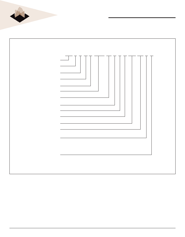
FUNCTIONAL BLOCK DIAGRAM
A0
Serial PD
A1
A2
SA0 SA1 SA2
SCL
SDA
WP
V
CCSPD
V
CC
/V
CCQ
V
REF
V
SS
Serial PD
DDR2 SDRAMs
DDR2 SDRAMs
DDR2 SDRAMs
P
L
L
OE
CK0
CK0#
RESET#
PCK0-PCK6, PCK8, PCK9
CK : DDR2 SDRAMs
PCK0#-PCK6#, PCK8#, PCK9#
CK# : DDR2 SDRAMs
PCK7
CK : Register
PCK7#
CK# : Register
V
SS
RCS1#
RCS0#
DQD
DQ1
DQ2
DQ3
I/O 0
I/O 1
I/O 2
I/O 3
DM
CS# DQS DQS#
DQS0
DQS0#
DQS1
DQS1#
DQ8
DQ9
DQ10
DQ11
I/O 0
I/O 1
I/O 2
I/O 3
DM
CS# DQS DQS#
DQS2
DQS2#
DQ16
DQ17
DQ18
DQ19
I/O 0
I/O 1
I/O 2
I/O 3
DM
CS# DQS DQS#
DQS3
DQS3#
DQ24
DQ25
DQ26
DQ27
I/O 0
I/O 1
I/O 2
I/O 3
DM
CS# DQS DQS#
DQS4
DQS4#
DQ32
DQ33
DQ34
DQ35
I/O 0
I/O 1
I/O 2
I/O 3
DM
CS# DQS DQS#
DQS5
DQS5#
DQ40
DQ41
DQ42
DQ43
I/O 0
I/O 1
I/O 2
I/O 3
DM
CS# DQS DQS#
DQS6
DQS6#
DQ48
DQ49
DQ50
DQ51
I/O 0
I/O 1
I/O 2
I/O 3
DM
CS# DQS DQS#
DQS7
DQS7#
DQ56
DQ57
DQ58
DQ59
I/O 0
I/O 1
I/O 2
I/O 3
DM
CS# DQS DQS#
DQS8
DQS8#
CB0
CB1
CB2
CB3
I/O 0
I/O 1
I/O 2
I/O 3
DM
CS# DQS DQS#
I/O 0
I/O 1
I/O 2
I/O 3
DM
CS# DQS DQS#
I/O 0
I/O 1
I/O 2
I/O 3
DM
CS# DQS DQS#
I/O 0
I/O 1
I/O 2
I/O 3
DM
CS# DQS DQS#
I/O 0
I/O 1
I/O 2
I/O 3
DM
CS# DQS DQS#
I/O 0
I/O 1
I/O 2
I/O 3
DM
CS# DQS DQS#
I/O 0
I/O 1
I/O 2
I/O 3
DM
CS# DQS DQS#
I/O 0
I/O 1
I/O 2
I/O 3
DM
CS# DQS DQS#
I/O 0
I/O 1
I/O 2
I/O 3
DM
CS# DQS DQS#
I/O 0
I/O 1
I/O 2
I/O 3
DM
CS# DQS DQS#
DQS9
DQS9#
DQ4
DQ5
DQ6
DQ7
I/O 0
I/O 1
I/O 2
I/O 3
DM
CS# DQS DQS#
DQS10
DQS10#
DQ12
DQ13
DQ14
DQ15
I/O 0
I/O 1
I/O 2
I/O 3
DM
CS# DQS DQS#
DQS11
DQS11#
DQ20
DQ21
DQ22
DQ23
I/O 0
I/O 1
I/O 2
I/O 3
DM
CS# DQS DQS#
DQS12
DQS12#
DQ28
DQ29
DQ30
DQ31
I/O 0
I/O 1
I/O 2
I/O 3
DM
CS# DQS DQS#
DQS13
DQS13#
DQ36
DQ37
DQ38
DQ39
I/O 0
I/O 1
I/O 2
I/O 3
DM
CS# DQS DQS#
DQS14
DQS14#
DQ44
DQ45
DQ46
DQ47
I/O 0
I/O 1
I/O 2
I/O 3
DM
CS# DQS DQS#
DQS15
DQ15#
DQ52
DQ53
DQ54
DQ55
I/O 0
I/O 1
I/O 2
I/O 3
DM
CS# DQS DQS#
DQS16
DQ16#
DQ60
DQ61
DQ62
DQ63
I/O 0
I/O 1
I/O 2
I/O 3
DM
CS# DQS DQS#
DQS17
DQ17#
CB4
CB5
CB6
CB7
I/O 0
I/O 1
I/O 2
I/O 3
DM
CS# DQS DQS#
I/O 0
I/O 1
I/O 2
I/O 3
DM
CS# DQS DQS#
I/O 0
I/O 1
I/O 2
I/O 3
DM
CS# DQS DQS#
I/O 0
I/O 1
I/O 2
I/O 3
DM
CS# DQS DQS#
I/O 0
I/O 1
I/O 2
I/O 3
DM
CS# DQS DQS#
I/O 0
I/O 1
I/O 2
I/O 3
DM
CS# DQS DQS#
I/O 0
I/O 1
I/O 2
I/O 3
DM
CS# DQS DQS#
I/O 0
I/O 1
I/O 2
I/O 3
DM
CS# DQS DQS#
I/O 0
I/O 1
I/O 2
I/O 3
DM
CS# DQS DQS#
I/O 0
I/O 1
I/O 2
I/O 3
DM
CS# DQS DQS#
1:4
R
E
G
I
S
T
E
R
RST#
BA0 - BA1
A0 - A13
RAS#
CAS#
WE#
CKE0
CKE1
ODT0
ODT1
RESET#
PCK7
PCK7#
RCS0# CS#: DDR2 SDRAMs
RCS1# CS#: DDR2 SDRAMs
RBA0-RBA1# BA0-BA1 : DDR2 SDRAMs
RA0-RA13 A0-A13 : DDR2 SDRAMs
RRAS# RAS# : DDR2 SDRAMs
RCAS# CAS#: DDR2 SDRAMs
RWE# WE#: DDR2 SDRAMs
RCKE0 CKE : DDR2 SDRAMs
RCKE1 CKE : DDR2 SDRAMs
RODT0 DDR2 SDRAMs
RODT1 DDR2 SDRAMs
CS0#
CS1#
NOTE: All resistor values are 22 ohms unless otherwise specifi ed.
WV3HG2128M72AER-D6
ADVANCED*
4
White Electronic Designs Corporation ∑ (602) 437-1520 ∑ www.wedc.com
White Electronic Designs
September
2005 Rev. 0
DC OPERATING CONDITIONS
All voltages referenced to V
SS
Parameter
Symbol
Min
Typical
Max
Unit
Notes
Supply voltage
V
CC
1 .7
1 .8
1 .9
V
1
I/O Supply voltage
V
CCQ
1 .7
1 .8
1 .9
V
4
V
CCL
Supply voltage
V
CCL
1 .7
1 .8
1 .9
V
4
I/O Reference voltage
V
REF
0.49 x V
CCQ
0.50 x V
CCQ
0.51 x V
CCQ
V
2
I/O Termination voltage
V
TT
V
REF
-0.04
V
REF
V
REF
+ 0.04
V
3
Notes:
1. V
CC
V
CCQ
must track each other. V
CCQ
must be less than or equal to V
CC
.
2. V
REF
is expected to equal V
CCQ
/2 of the transmitting device and to track variations in the DC level of the same. Peak-to-peak noise on V
REF
may not exceed ±1 percent of the DC
value. Peak-to-peak AC noise on V
REF
may not exceed ±2 percent of V
REF
. This measurement is to be taken at the nearest V
REF
bypass capacitor.
3. V
TT
is not applied directly to the device. V
TT
is a system supply for signal termination resistors, is expected to be set equal to V
REF
and must track variations in the DC level of V
REF
.
4. V
CCQ
tracks with V
CC
; V
CCL
track with V
CC
.
ABSOLUTE MAXIMUM RATINGS
Symbol
Parameter
MIN
MAX
U nit
V
CC
Voltage on V
CC
pin relative to V
SS
-1.0
2.3
V
V
CCQ
Voltage on V
CCQ
pin relative to V
SS
-0.5
2.3
V
V
CCL
Voltage on V
CCL
pin relative to V
SS
-0.5
2.3
V
V
IN
, V
OUT
Voltage on any pin relative to V
SS
-0.5
2.3
V
T
STG
Storage temperature
-55
100
∞C
I
L
Input leakage current; Any input 0V<V
IN
<V
CC
; V
REF
input
0V<V
IN
<0.95V; Other pins not under test = 0V
Command/Address,
RAS#, CAS#, WE#,
CS#, CKE
CK, CK#
DM
-5
5
uA
I
OZ
Output leakage current;
0V<V
OUT
<V
CCQ
; DQs and ODT are disable
DQ, DQS, DQS#
-10
-10
uA
I
VREF
V
REF
leakage current; V
REF
= Valid V
REF
level
-72
72
uA
CAPACITANCE
TA=25∞C, f=1MHz, V
CC =
V
CCQ =
1.8V
Parameter
Symbol
Min
Max
Unit
Input capacitance (A0 ~ A1 3, BA0 ~ BA1 ,RAS#,CAS#,WE#)
C
IN1
9
11
pF
Input capacitance ( CKE0, CKE1), (ODT0, ODT1)
C
IN2
9
11
pF
Input capacitance (CS0#, CS1#)
C
IN3
14
18
pF
Input capacitance (CK0, CK0#)
C
IN4
6
7
pF
Input capacitance (DQS0 ~ DQS8)
C
IN5
9
12
pF
Input capacitance (DQ0 ~ DQ63), (CB0 ~ CB7)
C
OUT1
9
12
pF
WV3HG2128M72AER-D6
ADVANCED*
5
White Electronic Designs Corporation ∑ (602) 437-1520 ∑ www.wedc.com
White Electronic Designs
September
2005 Rev. 0
OPERATING TEMPERATURE CONDITION
Parameter
Symbol
Rating
Units
Notes
Operating temperature
T
OPER
0 to 85
∞C
1, 2
Notes:
1. Operating temperature is the case surface temperature on the center/top side of the DRAM. For the measurement conditions, please refer to JEDEC JESD51 .2
2. At 0 - 85∞C, operation temperature range, all DRAM specifi cation will be supported.
INPUT DC LOGIC LEVEL
All voltages referenced to V
SS
Parameter
Symbol
Min
Max
Unit
Input High (Logic 1 ) Voltage
V
IH
(DC)
V
REF
+ 0.1 25
V
REF
+ 0.300
V
Input Low (Logic 0) Voltage
V
IL
(DC)
-0.300
V
REF
- 0.125
V
INPUT AC LOGIC LEVEL
All voltages referenced to V
SS
Parameter
Symbol
Min
Max
Unit
AC Input High (Logic 1 ) Voltage
V
IH
(AC)
V
REF
+ 0.250
--
V
AC Input Low (Logic 0) Voltage DDR2-400 & DDR2-533
V
IL
(AC)
--
V
REF
- 0.250
V
WV3HG2128M72AER-D6
ADVANCED*
6
White Electronic Designs Corporation ∑ (602) 437-1520 ∑ www.wedc.com
White Electronic Designs
September
2005 Rev. 0
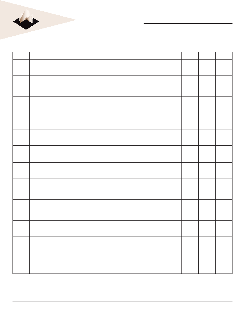
DDR2 I
DD
SPECIFICATIONS AND CONDITIONS
Includes DDR2 SDRAM components only
Symbol
Proposed Conditions
534
403
Units
I
DD0*
Operating one bank active-precharge current;
t
CK
= t
CK
(I
DD
), t
RC
= t
RC
(I
DD
), t
RAS
= t
RAS
min(I
DD
); CKE is HIGH, CS# is HIGH between valid commands;
Address bus inputs are SWITCHING; Data bus inputs are SWITCHING
2284
2284
mA
I
DD1*
Operating one bank active-read-precharge current;
I
OUT
= 0mA; BL = 4, CL = CL(I
DD
), AL = 0; t
CK
= t
CK
(I
DD
), t
RC
= t
RC
(I
DD
), t
RAS
= t
RAS
min(I
DD
), t
RCD
= t
RCD
(I
DD
);
CKE is HIGH, CS# is HIGH between valid commands; Address bus inputs are SWITCHING; Data bus input
are switching; Data pattern is same as I
DD
6W
2554
2554
mA
I
DD2P**
Precharge power-down current;
All banks idle; t
CK
= t
CK
(I
DD
); CKE is LOW; Other control and address bus inputs are STABLE; Data bus
inputs are FLOATING
988
988
mA
I
DD2Q**
Precharge quiet standby current;
All banks idle; t
CK
= t
CK
(I
DD
); CKE is HIGH, CS# is HIGH; Other control and address bus inputs are STABLE;
Data bus inputs are FLOATING
1780
1780
mA
I
DD2N**
Precharge standby current;
All banks idle; t
CK
= t
CK
(I
DD
); CKE is HIGH, CS# is HIGH; Other control and address bus inputs are
SWITCHING; Data bus inputs are SWITCHING
1960
1960
mA
I
DD3P**
Active power-down current;
All banks open; t
CK
= t
CK
(I
DD
); CKE is LOW; Other control and address
bus inputs are STABLE; Data bus inputs are FLOATING
Fast PDN Exit MRS(12) = 0mA
1780
1780
mA
Slow PDN Exit MRS(12) = 1mA
1132
1132
mA
I
DD3N**
Active standby current;
All banks open; t
CK
= t
CK
(I
DD
), t
RC
= t
RC
(I
DD
); t
RAS
= t
RAS
max(I
DD
); CKE is HIGH, CS# is HIGH between valid
commands; Other control and address bus inputs are SWITCHING; Data bus inputs are SWITCHING
2500
2500
mA
I
DD4W*
Operating burst write current;
All banks open, Continuous burst writes; BL = 4, CL = CL(I
DD
), AL = 0; t
CK
= t
CK
(I
DD
), t
RAS
= t
RAS
max(I
DD
), t
RP
= t
RP
(I
DD
); CKE is HIGH, CS# is HIGH between valid commands; Address bus inputs are SWITCHING; Data
bus inputs are SWITCHING
2824
2644
mA
I
DD4R*
Operating burst read current;
All banks open, Continuous burst reads, I
OUT
= 0mA; BL = 4, CL = CL(I
DD
), AL = 0; t
CK
= t
CK
(I
DD
), t
RAS
=
t
RAS
max(I
DD
), t
RP
= t
RP
(I
DD
); CKE is HIGH, CS# is HIGH between valid commands; Address bus inputs are
SWITCHING; Data pattern is same as I
DD
4W
2914
2734
mA
I
DD5**
Burst auto refresh current;
t
CK
= t
CK
(I
DD
); Refresh command at every t
RFC
(I
DD
) interval; CKE is HIGH, CS# is HIGH between valid
commands; Other control and address bus inputs are SWITCHING; Data bus inputs are SWITCHING
5740
5740
mA
I
DD6**
Self refresh current;
CK and CK# at 0V; CKE 0.2V; Other control and address bus inputs
are FLOATING; Data bus inputs are FLOATING
Normal
288
288
mA
I
DD7*
Operating bank interleave read current;
All bank interleaving reads, I
OUT
= 0mA; BL = 4, CL = CL(I
DD
), AL = t
RC
D(I
DD
)-1*t
CK
(I
DD
); t
CK
= t
CK
(I
DD
), t
RC
=
t
RC
(I
DD
), t
RRD
= t
RRD
(I
DD
), t
RCD
= 1*t
CK
(I
DD
); CKE is HIGH, CS# is HIGH between valid commands; Address
bus inputs are STABLE during DESELECTs; Data bus imputs are switching.
4804
4804
mA
Notes:
I
DD
specifi cation is based on SAMSUNG components. Other DRAM manufacturers specifi cation may be different.
* Value calculated as one module rank in this operating condition, and all other module ranks in I
DD2P
( CKE LOW) mode.
** Value calculated refl ects all module ranks in this operating condition.

WV3HG2128M72AER-D6
ADVANCED*
7
White Electronic Designs Corporation ∑ (602) 437-1520 ∑ www.wedc.com
White Electronic Designs
September
2005 Rev. 0
AC TIMING PARAMETERS & SPECIFICATIONS
0∞C T
A
+70∞C; V
CCQ
= + 1.8V ± 0.1V, V
CC
= +1.8V ± 0.1V
AC CHARACTERISTICS
534
403
PARAMETER
SYMBOL
MIN
MAX
MIN
MAX
UNIT
Clock
Clock cycle time
CL = 4
t
CK (4)
3,750
8,000
5,000
8,000
ps
CL = 3
t
CK (3)
5,000
8,000
5,000
8,000
ps
CK high-level width
t
CH
0.45
0.55
0.45
0.55
t
CK
CK low-level width
t
CL
0.45
0.55
0.45
0.55
t
CK
Half clock period
t
HP
MIN (t
CH
, t
CL
)
MIN (t
CH
, t
CL
)
ps
Clock jitter
t
JIT
TBD
TBD
ps
Data
DQ output access time from CK/CK#
t
AC
-500
+500
-600
+600
ps
Data-out high-impedance window from CK/CK#
t
HZ
t
AC
MAX
t
AC
MAX
ps
Data-out low-impedance window from CK/CK#
t
LZ
t
AC
MIN
t
AC
MAX
t
AC
MIN
t
AC
MAX
ps
DQ and DM input setup time relative to DQS
t
DS
100
150
DQ and DM input hold time relative to DQS
t
DH
225
275
A DQ and DM input pulse width (for each input)
t
D
I
PW
0.35
0.35
t
CK
Data hold skew factor
t
QHS
400
450
ps
DQ...DQS hold, DQS to fi rst DQ to go nonvalid, per access
t
QH
t
HP
- t
QHS
t
HP
- t
QHS
ps
Data valid output window (DVW)
t
DVW
t
QH
- t
DQSQ
t
QH
- t
DQSQ
ns
Data Strobe
DQS input high pulse width
t
DQSH
0.35
0.35
t
CK
DQS input low pulse width
t
DQSL
0.35
0.35
t
CK
DQS output access time from CK/CK#
t
DQSCK
-450
+450
-500
+500
ps
DQS falling edge to CK rising ... setup time
t
DSS
0.2
0.2
t
CK
DQS falling edge from CK rising ... hold time
t
DSH
0.2
0.2
t
CK
DQS...DQ skew, DQS to last DQ valid, per group,
per access
t
DQSQ
300
350
ps
DQS read preamble
t
RPRE
0.9
1.1
0.9
1.1
t
CK
DQS read postamble
t
RPST
0.4
0.6
0.4
0.6
t
CK
DQS write preamble setup time
t
WPRES
0
0
ps
DQS write preamble
t
WPRE
0.35
0.35
t
CK
DQS write postamble
t
WPST
0.4
0.6
0.4
0.6
t
CK
Write command to fi rst DQS latching transition
t
DQSS
WL - 0.25
WL + 0.25
WL - 0.25
WL + 0.25
t
CK
Notes:
AC specifi cation is based on SAMSUNG components. Other DRAM manufacturers specifi cation may be different.
Continued on next page

WV3HG2128M72AER-D6
ADVANCED*
8
White Electronic Designs Corporation ∑ (602) 437-1520 ∑ www.wedc.com
White Electronic Designs
September
2005 Rev. 0
AC TIMING PARAMETERS (cont'd)
0∞C T
A
+70∞C; V
CCQ
= + 1.8V ± 0.1V, V
CC
= +1.8V ± 0.1V
AC CHARACTERISTICS
534
403
PARAMETER
SYMBOL
MIN
MAX
MIN
MAX
UNIT
Command and
Address
Address and control input pulse width for each input
t
IPW
0.6
0.6
t
CK
Address and control input setup time
t
IS
250
250
ps
Address and control input hold time
t
IH
375
475
ps
CAS# to CAS# command delay
t
CCD
2
2
t
CK
ACTIVE to ACTIVE (same bank) command
t
RC
60
65
ns
ACTIVE bank a to ACTIVE bank b command
t
RRD
7.5
7.5
ns
ACTIVE to READ or WRITE delay
t
RCD
15
15
ns
Four Bank Activate period
t
FAW
37.5
37.5
37.5
37.5
ns
ACTIVE to PRECHARGE command
t
RAS
45
70,000
45
70,000
ns
Internal READ to precharge command delay
t
RTP
7.5
7.5
ns
Write recovery time
t
WR
15
15
ns
Auto precharge write recovery + precharge time
t
DAL
t
WR
+ t
RP
t
WR
+ t
RP
ns
Internal WRITE to READ command delay
t
WTR
7.5
10
ns
PRECHARGE command period
t
RP
15
15
ns
PRECHARGE all command period
t
RPA
t
RP
+ t
CK
t
RP
+ t
CK
ns
LOAD MODE command cycle time
t
MRD
2
2
t
CK
CKE low to CK,CK# uncertainty
t
DELAY
4.375
4.375
ns
Self Refresh
REFRESH to REFRESH command interval
t
RFC
127.5
70,000
127.5
70,000
ns
Average periodic refresh interval
t
REFI
7.8
7.8
µs
Exit self refresh to non-READ command
t
XSNR
t
RFC
(MIN)
+ 10
t
RFC (MIN)
+ 10
ns
Exit self refresh to READ command
t
XSRD
200
200
t
CK
Exit self refresh timing reference
t
ISXR
t
IS
t
IS
ps
ODT
ODT turn-on delay
t
AOND
2
2
2
2
t
CK
ODT turn-on
t
AON
t
AC
(MIN)
t
AC
(MAX) +
1000
t
AC
(MIN)
t
AC
(MAX) +
1000
ps
ODT turn-off delay
t
AOFD
2.5
2.5
2.5
2.5
t
CK
ODT turn-off
t
AOF
t
AC
(MIN)
t
AC
(MAX) +
600
t
AC
(MIN)
t
AC
(MAX) +
600
ps
ODT turn-on (power-down mode)
t
AONPD
t
AC
(MIN) +
2000
2 x t
CK
+
t
AC
(MAX) +
1000
t
AC
(MIN) +
2000
2 x t
CK
+
t
AC
(MAX) +
1000
ps
ODT turn-off (power-down mode)
t
AOFPD
t
AC
(MIN) +
2000
2.5 x t
CK
+
t
AC
(MAX) +
1000
t
AC
(MIN) +
2000
2.5 x t
CK
+
t
AC
(MAX) +
1000
ps
ODT to power-down entry latency
t
ANPD
3
3
t
CK
ODT power-down exit latency
t
AXPD
8
8
t
CK
Power-Down
Exit active power-down to READ command, MR[bit12=0]
t
XARD
2
2
t
CK
Exit active power-down to READ command, MR[bit12=1]
t
XARDS
6 - AL
6 - AL
t
CK
A Exit precharge power-down to any non-READ command.
t
XP
2
2
t
CK
CKE minimum high/low time
t
CKE
3
3
t
CK
Notes:
AC specifi cation is based on SAMSUNG components. Other DRAM manufacturers specifi cation may be different.

WV3HG2128M72AER-D6
ADVANCED*
9
White Electronic Designs Corporation ∑ (602) 437-1520 ∑ www.wedc.com
White Electronic Designs
September
2005 Rev. 0
133.35 (5.25)
133.20 (5.244)
Front View
Back View
3.00
(0.118)
(4x)
63.00 (2.48)
TYP
55.00 (2.165)
TYP
PIN 240
PIN 121
5.0 (0.197) TYP.
PIN 1
PIN 120
2.50
(0.098)
1.00
(0.039)
0.20
(0.008)
Detail B
Detail B
5.00 (0.197) TYP.
Detail A
1.69 0 (0.063)
1.40 (0.055)
0.85 (0.034)
0.75 (0.030)
Detail C
Detail A
4.843 (123.0)
TYP.
Detail C
3.00
(0.118)
(4X)
4.00
(0.157)
(4X)
5.175 (0.204)
(2x)
30.50 (1.201)
29.85 (1.175)
17.80 (0.700)
TYP.
10.00 (0.394)
TYP.
3.80 (0.150)
4.00 (0.157)
MAX
1.37 (0.054)
1.17 (0.046)
2.70 (0.106
2.30 (0.091)
PACKAGE DIMENSIONS FOR D6
* ALL DIMENSIONS ARE IN MILLIMETERS AND (INCHES)
ORDERING INFORMATION FOR D6
Part Number
Speed
CAS Latency
t
RCD
t
RP
Height*
WV3HG2128M72AER534D6xG
266MHz/533Mb/s
4
4
4
29.97mm (1.18")
WV3HG2128M72AER403D6xG
200MHz/400Mb/s
3
3
3
29.97mm (1.18")
NOTES:
∑ RoHS products. ("G" = RoHS Compliant)
∑ Vendor specifi c part numbers are used to provide memory component source control. The place holder for this is shown as a lower case "x"
in the part numbers above and is to be replaced with respective vendors code. Consult factory for qualifi ed sourcing options.
(M = Micron, S = Samsung & consult factory for others)
∑ Consult factory for availability of industrial temperature (-40∞C to 85∞C) option
WV3HG2128M72AER-D6
ADVANCED*
10
White Electronic Designs Corporation ∑ (602) 437-1520 ∑ www.wedc.com
White Electronic Designs
September
2005 Rev. 0
PART NUMBERING GUIDE
WV 3 H G 2 128M 72 A E R xxx D6 x G
WEDC
MEMORY (SDRAM)
DDR 2
GOLD
RANK
DEPTH
BUS WIDTH
COMPONENT WIDTH (x4)
1.8V
REGISTERED
SPEED (MHz)
PACKAGE 240 PIN
COMPONENT VENDOR
NAME
(M = Micron)
(S = Samsung)
G = ROHS COMPLIANT

WV3HG2128M72AER-D6
ADVANCED*
11
White Electronic Designs Corporation ∑ (602) 437-1520 ∑ www.wedc.com
White Electronic Designs
September
2005 Rev. 0
Document Title
2GB ≠ 2x128Mx72 DDR2 SDRAM REGISTERED, w/PLL
Revision History
Rev #
History
Release Date
Status
Rev 0
Created
September 2005
Advanced