WV3HG64M32EEU-D4
May 2006
Rev. 2
ADVANCED*
1
White Electronic Designs Corporation ∑ (602) 437-1520 ∑ www.wedc.com
White Electronic Designs
256MB ≠ 64Mx32 DDR2 SDRAM UNBUFFERED
DESCRIPTION
The WV3HG64M32EEU is a 64Mx32 Double Data Rate
2 SDRAM memory module based on 512Mb DDR2
SDRAM components. The module consists of four 64Mx8,
in FBGA package mounted on a 200 pin SO-DIMM FR4
substrate.
* This product is under development, is not qualifi ed or characterized and is subject to
change or cancellation without notice.
NOTE: Consult factory for availability of:
∑ Vendor source control options
∑ Industrial temperature option
FEATURES
200-pin,
Small-Outline
DIMM
(SO-DIMM)
Fast data transfer rates: PC2-5300*, PC2-4200 and
PC2-3200
Utilizes 667*, 533 and 400 Mb/s DDR2 SDRAM
components
V
CC
= 1.8V ±0.1V
V
CCSPD
= 1.7V to 3.6V
JEDEC standard 1.8V I/O (SSTL_18-compatible)
Differential data strobe (DQS, DQS#) option
Four-bit
prefetch
architecture
DLL to align DQ and DQS transitions with CK
Multiple internal device banks for concurrent
operation
Supports duplicate output strobe (RDQS/RDQS#)
Programmable CAS# latency (CL): 3, 4, and 5
Programmable burst: length (4, 8)
Adjustable data-output drive strength
On-die
termination
(ODT)
Serial Presence Detect (SPD) with EEPROM
Auto & self refresh (64ms: 8,192 cycle refresh)
Row Addr: A0~A13, Column Addr: A0~A9,
Bank
Addr:
BA0~BA1
Gold edge contacts
RoHS
Compliant
JEDEC
Package
option
∑ 200 Pin (SO-DIMM)
∑ PCB ≠ 30.00mm (1.181") TYP.
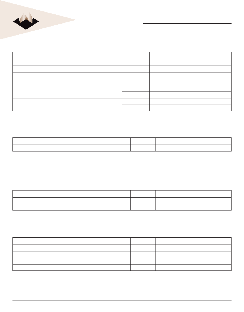
OPERATING FREQUENCIES
PC2-5300*
PC2-4200
PC2-3200
Clock Speed
333MHz
266MHz
200MHz
CL-t
RCD
-t
RP
5-5-5
4-4-4
3-3-3
Note:
∑ Consult factory for availability
WV3HG64M32EEU-D4
May 2006
Rev. 2
ADVANCED
2
White Electronic Designs Corporation ∑ (602) 437-1520 ∑ www.wedc.com
White Electronic Designs
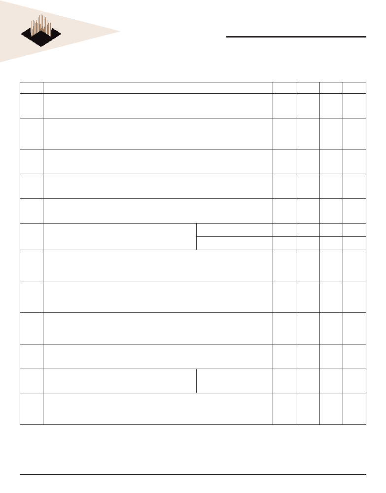
PIN NAMES
SYMBOL
DESCRIPTION
A0-A13
Address input
ODT0
On-Die Termination
CK0, CK0#
Differential Clock Inputs
CKE0
Clock Enable input
CS0#
Chip select
RAS#, CAS#, WE# Command Inputs
BA0, BA1
Bank Address Inputs
DM0-DM3
Input Data Mask
A10/AP
Address input/Auto precharge
DQ0-DQ31
Data Input/Output
DQS0-DQS3
DQS0#-DQS3#
Data Strobe
SCL
Serial Clock for Presence Detect
SA0-SA1
Presence Detect Address Inputs
SDA
Serial Presence Detect Data
V
CC
Power Supply: +1.8V ±0.1V
V
REF
SSTL_18 reference voltage
V
SS
Ground
V
CCSPD
Serial EEPROM Positive Power
Supply
NC
No Connect
PIN CONFIGURATION
PIN#
SYMBOL
PIN#
SYMBOL
PIN#
SYMBOL
PIN#
SYMBOL
1
VREF
51
DQS2
101
A1
151
NC
2
V
SS
52
DM2
102
A0
152
NC
3
V
SS
53
V
SS
103
VCC
153
NC
4
DQ4
54
V
SS
104
VCC
154
NC
5
DQ0
55
DQ18
105
A10/AP
155
V
SS
6
DQ5
56
DQ22
106
BA1
156
V
SS
7
DQ1
57
DQ19
107
BA0
157
NC
8
V
SS
58
DQ23
108
RAS#
158
NC
9
V
SS
59
V
SS
109
WE#
159
NC
10
DM0
60
V
SS
110
CS0#
160
NC
11
DQS0#
61
DQ24
111
VCC
161
V
SS
12
V
SS
62
DQ28
112
VCC
162
V
SS
13
DQS0
63
DQ25
113
CAS#
163
NC
14
DQ6
64
DQ29
114
ODT0
164
NC
15
V
SS
65
V
SS
115
NC
165
V
SS
16
DQ7
66
V
SS
116
A13
166
NC
17
DQ2
67
DM3
117
VCC
167
NC
18
V
SS
68
DQS3#
118
VCC
168
V
SS
19
DQ3
69
NC
119
NC
169
NC
20
DQ12
70
DQS3
120
NC
170
NC
21
V
SS
71
V
SS
121
V
SS
171
V
SS
22
DQ13
72
V
SS
122
V
SS
172
V
SS
23
DQ8
73
DQ26
123
NC
173
NC
24
V
SS
74
DQ30
124
NC
174
NC
25
DQ9
75
DQ27
125
NC
175
NC
26
DM1
76
DQ31
126
NC
176
NC
27
V
SS
77
V
SS
127
V
SS
177
V
SS
28
V
SS
78
V
SS
128
V
SS
178
V
SS
29
DQS1#
79
CKE0
129
NC
179
NC
30
CK0
80
NC
130
NC
180
NC
31
DQS1
81
VCC
131
NC
181
NC
32
CK0#
82
VCC
132
V
SS
182
NC
33
V
SS
83
NC
133
V
SS
183
V
SS
34
V
SS
84
NC
134
NC
184
V
SS
35
DQ10
85
NC
135
NC
185
NC
36
DQ14
86
NC
136
NC
186
NC
37
DQ11
87
VCC
137
NC
187
V
SS
38
DQ15
88
VCC
138
V
SS
188
NC
39
V
SS
89
A12
139
V
SS
189
NC
40
V
SS
90
A11
140
NC
190
V
SS
41
V
SS
91
A9
141
NC
191
NC
42
V
SS
92
A7
142
NC
192
NC
43
DQ16
93
A8
143
NC
193
V
SS
44
DQ20
94
A6
144
V
SS
194
NC
45
DQ17
95
VCC
145
V
SS
195
SDA
46
DQ21
96
VCC
146
NC
196
V
SS
47
V
SS
97
A5
147
NC
197
SCL
48
V
SS
98
A4
148
NC
198
SA0
49
DQS2#
99
A3
149
V
SS
199
VCCSPD
50
NC
100
A2
150
V
SS
200
SA1
WV3HG64M32EEU-D4
May 2006
Rev. 2
ADVANCED
3
White Electronic Designs Corporation ∑ (602) 437-1520 ∑ www.wedc.com
White Electronic Designs
FUNCTIONAL BLOCK DIAGRAM
DQ
DQ
DQ
DQ
DQ
DQ
DQ
DQ
DQ0
DQ1
DQ2
DQ3
DQ4
DQ5
DQ6
DQ7
DM CS#DQS DQS#
DQ
DQ
DQ
DQ
DQ
DQ
DQ
DQ
DQ8
DQ9
DQ10
DQ11
DQ12
DQ13
DQ14
DQ15
DM CS# DQS DQS#
DQ
DQ
DQ
DQ
DQ
DQ
DQ
DQ
DQ16
DQ17
DQ18
DQ19
DQ20
DQ21
DQ22
DQ23
DM CS# DQS DQS#
DQ
DQ
DQ
DQ
DQ
DQ
DQ
DQ
DQ24
DQ25
DQ26
DQ27
DQ28
DQ29
DQ30
DQ31
DM CS# DQS DQS#
DQS0#
DQS0
DM0
CS0#
DQS1#
DQS1
DM1
DQS2#
DQS2
DM2
DQS3#
DQS3
DM3
DDR2 SDRAMs
DDR2 SDRAMs
CK0
CK0#
100
A0
Serial PD
A1
A2
SA0 SA1
SDA
SCL
WP
BA0-BA1
A0-A13
RAS#
CAS#
WE#
CKE0
ODT0
NOTE: All resistor value, are 22 ohms ± 5% unless otherwise specified.
BA0-BA1: DDR2 SDRAMs
A0-A13:
DDR2 SDRAMs
RAS#:
DDR2 SDRAMs
CAS#:
DDR2 SDRAMs
WE#:
DDR2 SDRAMs
CKE0:
DDR2 SDRAMs
ODT0:
DDR2 SDRAMs
V
CCSPD
V
CC
V
REF
V
SS
Serial PD
DDR2 SDRAMs
DDR2 SDRAMs
DDR2 SDRAMs
3
3
WV3HG64M32EEU-D4
May 2006
Rev. 2
ADVANCED
4
White Electronic Designs Corporation ∑ (602) 437-1520 ∑ www.wedc.com
White Electronic Designs
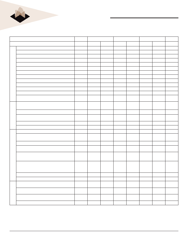
ABSOLUTE MAXIMUM RATINGS
Symbol
Parameter
Min
Max
Units
V
CC
Voltage on V
CC
pin relative to V
SS
-0.5
2.3
V
V
IN
, V
OUT
Voltage on any pin relative to V
SS
-0.5
2.3
V
T
STG
Storage Temperature
-55
100
∞C
I
L
Input leakage current; Any input 0V<V
IN
<V
CC
;
VREF
input
0V<V
IN
<0.95V; Other pins not under test = 0V
Command/Address,
RAS#, CAS#, WE#
-20
20
µA
CS#, CKE
-20
20
µA
CK, CK#
-20
20
µA
DM
-5
5
µA
I
OZ
Output leakage current; 0V<V
IN
<V
CC
; DQs and ODT are
disable
DQ, DQS, DQS#
-5
5
µA
I
VREF
V
REF
leakage current; V
REF
= Valid
VREF
level
-8
8
µA
DC OPERATING CONDITIONS
All voltages referenced to V
SS
Parameter
Symbol
Rating
Units
Notes
Min.
Type
Max.
Supply Voltage
V
CC
1.7
1.8
1.9
V
3
I/O Reference Voltage
V
REF
0.49 x V
CC
0.50 x V
CC
0.51 x V
CC
V
1
I/O Termination Voltage
V
TT
V
REF
-0.04
V
REF
V
REF
+0.04
V
2
Notes:
1. V
REF
is expected to equal V
CC
/2 of the transmitting device and to track variations in the DC level of the same. Peak-to-peak noise on V
REF
may not exceed +/-1 percent of the DC
value. Peak-to-peak AC noise on V
REF
may not exceed +/-2 percent of V
REF
. This measurement is to be taken at the nearest V
REF
bypass capacitor.
2. V
TT
in sot applied directly to the device.
V
TT
is a system supply for signal termination resistors, is expected to be set equal to V
REF
and must track variations in the DC level of V
REF
.
3. V
CCQ
of all IC's are tied to V
CC
.
WV3HG64M32EEU-D4
May 2006
Rev. 2
ADVANCED
5
White Electronic Designs Corporation ∑ (602) 437-1520 ∑ www.wedc.com
White Electronic Designs
INPUT/OUTPUT CAPACITANCE
T
A
= 25∞C, f = 100MHz
Parameter
Symbol
Min
Max
Units
Input Capacitance (A0~A13, BA0~BA1, RAS#, CAS#, WE#)
C
IN1
8
12
pF
Input Capacitance CKE0, ODT
C
IN2
8
12
pF
Input Capacitance CS0#
C
IN3
8
12
pF
Input Capacitance (CK0, CK0#)
C
IN4
8
12
pF
Input Capacitance (DM0 ~ DM3), (DQS0 ~ DQS3)
C
IN5
(665)
6.5
7.5
pF
C
IN5
(534)
6.5
8
pF
Input Capacitance (DQ0 ~ DQ31)
C
OUT1
(665)
6.5
7.5
pF
C
OUT1
(534)
6.5
8
pF
Notes:
∑ AC specifi cation is based on SAMSUNG components. Other DRAM manufactures specifi cation may be different.
OPERATING TEMPERATURE CONDITION
Parameter
Symbol
Rating
Units
Notes
Operating temperature (Commercial)
TOPER
0
∞
to 85∞
∞C
1, 2
Notes:
1. Operating temperature is the case surface temperature on the center/top side of the DRAM. For the measurement conditions, please refer to JEDED JESD51.2
2. At 0∞C - 85∞C, operation temperature range, all DRAM specifi cation will be supported.
INPUT DC LOGIC LEVEL
All voltages referenced to V
SS
Parameter
Symbol
Min
Max
Units
Input High (Logic 1) Voltage
V
IH
(DC)
V
REF
+ 0.125
V
CC
+ 0.300
V
Input Low (Logic 0) Voltage
V
IL
(DC)
-0.300
V
REF
- 0.125
V
INPUT AC LOGIC LEVEL
All voltages referenced to V
SS
Parameter
Symbol
Min
Max
Units
Input High (Logic 1) Voltage DDR2-400 & DDR2-533
V
IH
(AC)
V
REF
+ 0.250
-
V
Input Low (Logic 1) Voltage DDR2-667
V
IH
(AC)
V
REF
+ 0.200
-
V
Input Low (Logic 0) Voltage DDR2-400 & DDR2-533
V
IL
(AC)
-
V
REF
- 0.250
V
Input Low (Logic 0) Voltage DDR2-667
V
IL
(AC)
-
V
REF
- 0.200
V
WV3HG64M32EEU-D4
May 2006
Rev. 2
ADVANCED
6
White Electronic Designs Corporation ∑ (602) 437-1520 ∑ www.wedc.com
White Electronic Designs
I
CC
SPECIFICATION
V
CC
= +1.8V ± 0.1V
Symbol
Proposed Conditions
665
534
403
Units
I
CC0*
Operating one bank active-precharge;
t
CK
= t
CK
(I
CC
), t
RC
= t
RC
(I
CC
), t
RAS
= t
RAS
min(I
CC
); CKE is HIGH, CS# is HIGH between valid commands;
Address bus inputs are SWITCHING; Data bus inputs are SWITCHING
340
320
320
mA
I
CC1*
Operating one bank active-read-precharge;
I
OUT
= 0mA; BL = 4, CL = CL(I
CC
), AL = 0; t
CK
= t
CK
(I
CC
), t
RC
= t
RC
(I
CC
), t
RAS
= t
RAS
min(I
CC
); CKE is
HIGH, CS# is HIGH between valid commands; Address bus inputs are SWITCHING; Data pattern is
same as I
CC
4W
400
380
380
mA
I
CC2P**
Precharge power-down current;
All banks idle; t
CK
= t
CK
(I
CC
); CKE is LOW; Other control and address bus inputs are STABLE; Data bus
inputs are FLOATING
32
32
32
mA
I
CC2Q**
Precharge quiet standby current;
All banks idle; t
CK
= t
CK
(I
CC
); CKE is HIGH, CS# is HIGH; Other control and address bus inputs are
STABLE; Data bus inputs are FLOATING
140
120
120
mA
I
CC2N**
Precharge standby current;
All banks idle; t
CK
= t
CK
(I
CC
); CKE is HIGH, CS# is HIGH; Other control and address bus inputs are
STABLE; Data bus inputs are SWITCHING
160
140
140
mA
I
CC3P**
Active power-down current;
All banks open; t
CK
= t
CK
(I
CC
); CKE is LOW; Other control and
address bus inputs are STABLE; Data bus inputs are FLOATING
Fast PDN Exit MRS(12) = 0
120
120
120
mA
Slow PDN Exit MRS(12) = 1
48
48
48
mA
I
CC3N**
Active standby current;
All banks open; t
CK
= t
CK
(I
CC
), t
RC
= t
RC
(I
CC,
t
RAS
= t
RAS
min(I
CC
); CKE is HIGH, CS# is HIGH between
valid commands; Other control and address bus inputs are SWITCHING; Data bus inputs are
SWITCHING
220
200
200
mA
I
CC4W*
Operating burst write current;
All banks open, Continuous burst writes; BL = 4, CL = CL(I
CC
), AL = 0; t
CK
= t
CK
(I
CC
), t
RAS
= t
RAS
max(I
CC
),
t
RP
= t
RP
(I
CC
); CKE is HIGH, CS# is HIGH between valid commands; Address bus inputs are
SWITCHING; Data bus inputs are SWITCHING
560
480
440
mA
I
CC4R*
Operating burst read current;
All banks open, Continuous burst reads, I
OUT
= 0mA; BL = 4, CL = CL(I
CC
), AL = 0; t
CK
= t
CK
(I
CC
), t
RAS
=
t
RAS
max(I
CC
), t
RP
= t
RP
(I
CC
); CKE is HIGH, CS# is HIGH between valid commands; Address bus inputs
are SWITCHING; Data pattern is same as I
CC
4W
580
500
440
mA
I
CC5**
Burst auto refresh current;
t
CK
= t
CK
(I
CC
); Refresh command at every t
RFC
(I
CC
) interval; CKE is HIGH, CS# is HIGH between valid
commands; Other control and address bus inputs are SWITCHING; Data bus inputs are SWITCHING
600
560
560
mA
I
CC6**
Self refresh current;
CK and CK# at 0V; CKE 0.2V; Other control and address bus inputs
are FLOATING; Data bus inputs are FLOATING
Normal
32
32
32
mA
I
CC7*
Operating bank interleave read current;
All bank interlea
vin
g reads, I
OUT
= 0mA; BL = 4, CL = CL(I
CC
), AL = t
RC
D(I
CC
)-1*t
CK
(I
CC
); t
CK
= t
CK
(I
CC
),
t
RC
= t
RC
(I
CC
), t
RRD
= t
RRD
(I
CC
), t
RCD
= 1*t
CK
(I
CC
); CKE is HIGH, CS# is HIGH between valid commands;
Address bus inputs are STABLE during DESELECTs; Data bus inputs are SWITCHING.
880
880
880
mA
I
CC
specifi cation is based on SAMSUNG components. Other DRAM manufactures specifi cation may be different.
Note:
*: Value calculated as one module rank in this operating condition, and all other module ranks in I
CC2P
(CKE LOW) mode.
**: Value calculated refl ects all module ranks in this operating condition.
WV3HG64M32EEU-D4
May 2006
Rev. 2
ADVANCED
7
White Electronic Designs Corporation ∑ (602) 437-1520 ∑ www.wedc.com
White Electronic Designs
AC TIMING PARAMETERS & SPECIFICATIONS
AC CHARACTERISTICS
665
534
403
PARAMETER
SYMBOL
MIN
MAX
MIN
MAX
MIN
MAX
UNIT
CL = 5
t
CK (5)
3,000
8,000
ps
CL = 4
t
CK (4)
3,750
8,000
3,750
8,000
5,000
8,000
ps
CL = 3
t
CK (3)
5,000
8,000
5,000
8,000
5,000
8,000
ps
CK high-level width
t
CH
0.45
0.55
0.45
0.55
0.45
0.55
t
CK
CK low-level width
t
CL
0.45
0.55
0.45
0.55
0.45
0.55
t
CK
Half clock period
t
HP
MIN (t
CH
,
t
CL
)
MIN (t
CH
,
t
CL
)
MIN (t
CH
,
t
CL
)
ps
Clock jitter
t
J
I
T
-125
125
-125
125
-125
125
ps
Data
DQ output access time from CK/CK#
t
AC
-450
+450
-500
+500
-600
+600
ps
Data-out high-impedance window from CK/CK#
t
HZ
t
AC
MAX
t
AC
MAX
t
AC
MAX
ps
Data-out low-impedance window from CK/CK#
t
LZ
t
AC
MIN
t
AC
MAX
t
AC
MIN
t
AC
MAX
t
AC
MIN
t
AC
MAX
ps
DQ and DM input setup time relative to DQS
t
DS
100
100
150
ps
DQ and DM input hold time relative to DQS
t
DH
225
225
275
ps
DQ and DM input pulse width (for each input)
t
D
I
PW
0.35
0.35
0.35
t
CK
Data hold skew factor
t
QHS
340
400
450
ps
DQ...DQS hold, DQS to fi rst DQ to go nonvalid, per
access
t
QH
t
HP
- t
QHS
t
HP
- t
QHS
t
HP
- t
QHS
ps
Data valid output window (DVW)
t
DVW
t
QH
- t
DQSQ
t
QH
- t
DQSQ
t
QH
- t
DQSQ
ns
Data Strobe
DQS input high pulse width
t
DQSH
0.35
0.35
0.35
t
CK
DQS input low pulse width
t
DQSL
0.35
0.35
0.35
t
CK
DQS output access time from CK/CK#
t
DQSCK
-400
+400
-450
+450
-500
+500
ps
DQS falling edge to CK rising ... setup time
t
DSS
0.2
0.2
0.2
t
CK
DQS falling edge from CK rising ... hold time
t
DSH
0.2
0.2
0.2
t
CK
DQS...DQ skew, DQS to last DQ valid, per group,
per access
t
DQSQ
240
300
350
ps
DQS read preamble
t
RPRE
0.9
1.1
0.9
1.1
0.9
1.1
t
CK
DQS read postamble
t
RPST
0.4
0.6
0.4
0.6
0.4
0.6
t
CK
DQS write preamble setup time
t
WPRES
0
0
0
p s
DQS write preamble
t
WPRE
0.35
0.35
0.35
t
CK
DQS write postamble
t
WPST
0.4
0.6
0.4
0.6
0.4
0.6
t
CK
Write command to fi rst DQS latching transition
t
DQSS
WL
- 0.25
WL +
0.25
WL
- 0.25
WL +
0.25
WL
- 0.25
WL +
0.25
t
CK
Address and control input pulse width for each input
t
IPW
0.6
0.6
0.6
t
CK
Address and control input setup time
t
IS
200
250
350
ps
Address and control input hold time
t
IH
275
375
475
ps
Address and control input hold time
t
CCD
2
2
2
t
CK
Note:
AC specifi cation is based on SAMSUNG components. Other DRAM manufactures specifi cation may be different.
Continued on next page
WV3HG64M32EEU-D4
May 2006
Rev. 2
ADVANCED
8
White Electronic Designs Corporation ∑ (602) 437-1520 ∑ www.wedc.com
White Electronic Designs
AC TIMING PARAMETERS (cont'd)
AC CHARACTERISTICS
665
534
403
PARAMETER
SYMBOL
MIN
MAX
MIN
MAX
MIN
MAX
UNIT
Command and
Address
ACTIVE to ACTIVE (same bank) command
t
RC
55
60
65
ns
ACTIVE bank a to ACTIVE bank b command
t
RRD
7.5
7.5
7.5
ns
ACTIVE to READ or WRITE delay
t
RCD
15
15
15
ns
Four Bank Activate period
t
FAW
37.5
37.5
37.5
37.5
37.5
37.5
ns
ACTIVE to PRECHARGE command
t
RAS
45
70,000
45
70,000
45
70,000
ns
Internal READ to precharge command delay
t
RTP
7.5
7.5
7.5
ns
Write recovery time
t
WR
15
15
15
ns
Auto precharge write recovery + precharge time
t
DAL
t
WR
+ t
RP
t
WR
+ t
RP
t
WR
+ t
RP
ns
Internal WRITE to READ command delay
t
WTR
7.5
7.5
10
ns
PRECHARGE command period
t
RP
15
15
15
ns
PRECHARGE ALL command period
t
RPA
t
RP+
t
CK
t
RP+
t
CK
t
RP+
t
CK
ns
LOAD MODE command cycle time
t
MRD
2
2
2
t
CK
CKE low to CK,CK# uncertainty
t
DELAY
t
IS
+ t
CK
+ t
IH
t
IS
+ t
CK
+ t
IH
t
IS
+ t
CK
+ t
IH
ns
Self Refresh
REFRESH to Active of Refresh to Refresh command
interfal
t
RFC
105
70,000
105
70,000
105
70,000
ns
Average periodic refresh interval
t
REF
I
7.8
7.8
7.8
µs
Exit self refresh to non-READ command
t
XSNR
t
RFC
(MIN)
+ 10
t
RFC
(MIN)
+ 10
t
RFC
(MIN)
+ 10
ns
Exit self refresh to READ command
t
XSRD
200
200
200
t
CK
Exit self refresh timing reference
tI
SXR
t
IS
t
IS
t
IS
ps
ODT
ODT turn-on delay
t
AOND
2
2
2
2
2
2
t
CK
ODT turn-on
t
AON
t
AC
(MIN)
t
AC
(MAX)
+ 1000
t
AC
(MIN)
t
AC
(MAX)
+ 1000
t
AC
(MIN)
t
AC
(MAX)
+ 1000
ps
ODT turn-off delay
t
AOFD
2.5
2.5
2.5
2.5
2.5
2.5
t
CK
ODT turn-off
t
AOF
t
AC
(MIN)
t
AC
(MAX)
+ 600
t
AC
(MIN)
t
AC
(MAX)
+ 600
t
AC
(MIN)
t
AC
(MAX)
+ 600
ps
ODT turn-on (power-down mode)
t
AONPD
t
AC
(MIN)
+ 2000
2 x t
CK
+
t
AC
(MAX)
+ 1000
t
AC
(MIN)
+ 2000
2 x t
CK
+
t
AC
(MAX)
+ 1000
t
AC
(MIN)
+ 2000
2 x t
CK
+
t
AC
(MAX)
+ 1000
ps
ODT turn-off (power-down mode)
t
AOFPD
t
AC
(MIN)
+ 2000
2.5 x
t
CK
+ t
AC
(MAX) +
1000
t
AC
(MIN)
+ 2000
2.5 x
t
CK
+ t
AC
(MAX) +
1000
t
AC
(MIN)
+ 2000
2.5 x
t
CK
+ t
AC
(MAX) +
1000
ps
ODT to power-down entry latency
t
ANPD
3
3
3
t
CK
ODT power-down exit latency
t
AXPD
8
8
8
t
CK
Power-Down
Exit active power-down to READ command,
MR[bit12=0]
t
XARD
2
2
2
t
CK
Exit active power-down to READ command,
MR[bit12=1]
t
XARDS
7 - AL
6 - AL
6 - AL
t
CK
A Exit precharge power-down to any non-READ
command.
t
XP
2
2
2
t
CK
CKE minimum high/low time
t
CKE
3
3
3
t
CK
Note:
AC specifi cation is based on SAMSUNG components. Other DRAM manufactures specifi cation may be different.
WV3HG64M32EEU-D4
May 2006
Rev. 2
ADVANCED
9
White Electronic Designs Corporation ∑ (602) 437-1520 ∑ www.wedc.com
White Electronic Designs
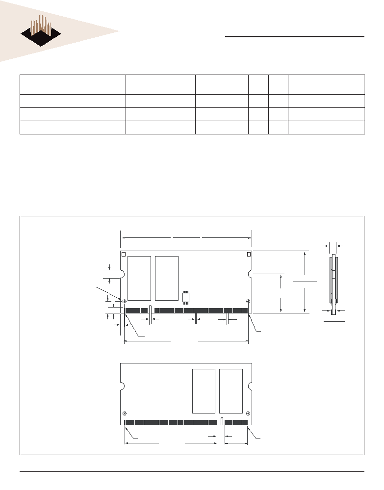
3.80 (0.150)
MAX
1.10 (0.043)
0.90 (0.035)
PIN 1
67.75 (2.667)
67.45 (2.656)
20.00 (0.787)
TYP
1.80 (0.071)
(2X)
0.60 (0.024)
TYP
0.45 (0.018)
TYP
PIN 199
PIN 200
PIN 2
2.15 (0.085)
6.00 (0.236)
63.60 (2.504)
2.55 (0.100)
1.00 (0.039)
TYP
TYP
BACK VIEW
FRONT VIEW
30.15 (1.187)
29.85 (1.175)
47.40 (1.866)
TYP
11.40 (0.449)
TYP
4.2 (0.165)
TYP
4.10(0.161) (2X)
3.90(0.154)
PACKAGE DIMENSIONS FOR D4
** ALL DIMENSIONS ARE IN MILLIMETERS AND (INCHES)
ORDERING INFORMATION FOR D4
Part Number
Clock/Data Rate
Frequency
CAS Latency
t
RCD
t
RP
Height**
WV3HG64M32EEU665D4xxG*
333MHz/667Mb/s
5
5
5
30.00mm (1.181") TYP
WV3HG64M32EEU534D4xxG
266MHz/533Mb/s
4
4
4
30.00mm (1.181") TYP
WV3HG64M32EEU403D4xxG
200MHz/400Mb/s
3
3
3
30.00mm (1.181") TYP
* Consult Factory for availability
NOTES:
∑ RoHS product. ("G" = RoHS Compliant)
∑ Vendor specifi c part numbers are used to provide memory components source control. The place holder for this is shown as lower case "x" in the part numbers above and is to be
replaced with the respective vendors code. Consult factory for qualifi ed sourcing options. (M = Micron, S = Samsung & consult factory for others)
∑ Consult factory for availability of industrial temperature (-40∞C to 85∞C) option
WV3HG64M32EEU-D4
May 2006
Rev. 2
ADVANCED
10
White Electronic Designs Corporation ∑ (602) 437-1520 ∑ www.wedc.com
White Electronic Designs
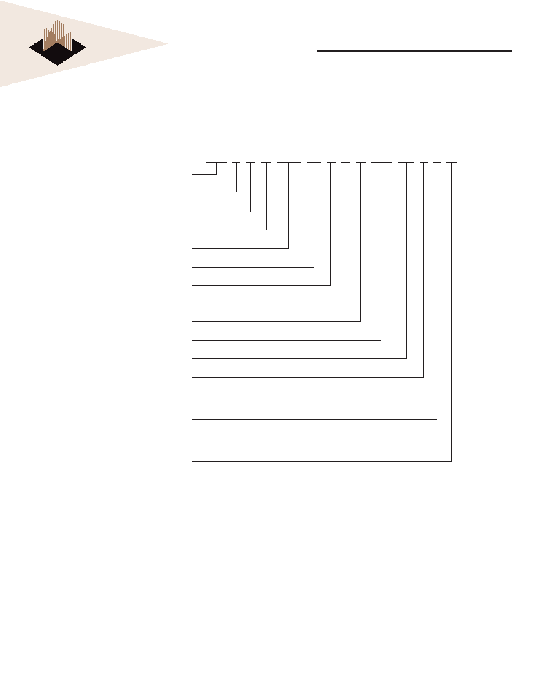
PART NUMBERING GUIDE
WV 3 H G 64M 32 E E U xxx D4 x x G
WEDC
MEMORY (SDRAM)
DDR 2
GOLD
DEPTH
BUS WIDTH
COMPONENT WIDTH x8
1.8V
UNBUFFERED
SPEED (Mb/s)
PACKAGE 200 PIN
INDUSTRIAL TEMP OPTION
(For commercial leave "blank"
for
industrial
add
"I")
COMPONENT VENDOR NAME
(M = Micron)
(S = Samsung)
G = RoHS COMPLIANT

WV3HG64M32EEU-D4
May 2006
Rev. 2
ADVANCED
11
White Electronic Designs Corporation ∑ (602) 437-1520 ∑ www.wedc.com
White Electronic Designs
Document Title
256MB ≠ 64Mx32 DDR2 SDRAM UNBUFFERED
DRAM DIE OPTIONS:
∑
SAMSUNG: C-Die, will move to E-Die Q2'06
∑
MICRON: U37Y: B-Die
Revision History
Rev #
History
Release Date
Status
Rev 0
Created
3-06
Advanced
Rev 1
1.1
Added row, column, and bank address
3-23-06
Advanced
Rev 2
2.1
Correction on component used, (512Mb)
2.2
Added V
CCQ
update
2.3
Added "x" to part number to indicate industrial temp option
2.4
Added "x" to part numbering guide to indicate industrial
temp option
2.5
Added die rev info
5-06 Advanced