PRELIMINARY
4Mb (256K x 16) Pseudo Static RAM
CG6257AM
Weida Semiconductor, Inc.
38-XXXXX
Revised August 2003
Features
∑ Wide voltage range: 2.70V≠3.30V
∑ Access Time: 70ns
∑ Ultra-low active power
-- Typical active current: 2.0mA @ f = 1 MHz
-- Typical active current: 13mA @ f = f
max
∑ Ultra low standby power
∑ Automatic power-down when deselected
∑ CMOS for optimum speed/power
∑ Offered in a 48 Ball BGA Package
Functional Description
[1]
The CG6257AM is a high-performance CMOS Pseudo static
RAM organized as 256K words by 16 bits that supports an
asynchronous memory interface. This device features
advanced circuit design to provide ultra-low active current.
This is ideal for providing More Battery Life
Æ
(MoBL) in
portable applications such as cellular telephones. The device
can be put into standby mode reducing power consumption by
more than 99% The device can also be put into standby mode
when deselected (CE HIGH or both BHE and BLE are HIGH).
The input/output pins (I/O
0
through I/O
15
) are placed in a
high-impedance state when: deselected (CE HIGH ), outputs
are disabled (OE HIGH), both Byte High Enable and Byte Low
Enable are disabled (BHE, BLE HIGH), or during a write
operation (CE LOW and WE LOW). The addresses must not
be toggled once the read is started on the device.
Writing to the device is accomplished by taking Chip Enables
(CE
LOW ) and Write Enable (WE) input LOW. If Byte Low
Enable (BLE) is LOW, then data from I/O pins (I/O
0
through
I/O
7
), is written into the location specified on the address pins
(A
0
through A
17
). If Byte High Enable (BHE) is LOW, then data
from I/O pins (I/O
8
through I/O
15
) is written into the location
specified on the address pins (A
0
through A
17
).
Reading from the device is accomplished by taking Chip
Enables (CE
LOW) and Output Enable (OE) LOW while
forcing the Write Enable (WE) HIGH. If Byte Low Enable (BLE)
is LOW, then data from the memory location specified by the
address pins will appear on I/O
0
to I/O
7
. If Byte High Enable
(BHE) is LOW, then data from memory will appear on I/O
8
to
I/O
15
. See the truth table at the back of this datasheet for a
complete description of read and write modes
Note:
1.
For best-practice recommendations, please refer to the Cypress application note "System Design Guidelines" on http://www.cypress.com.
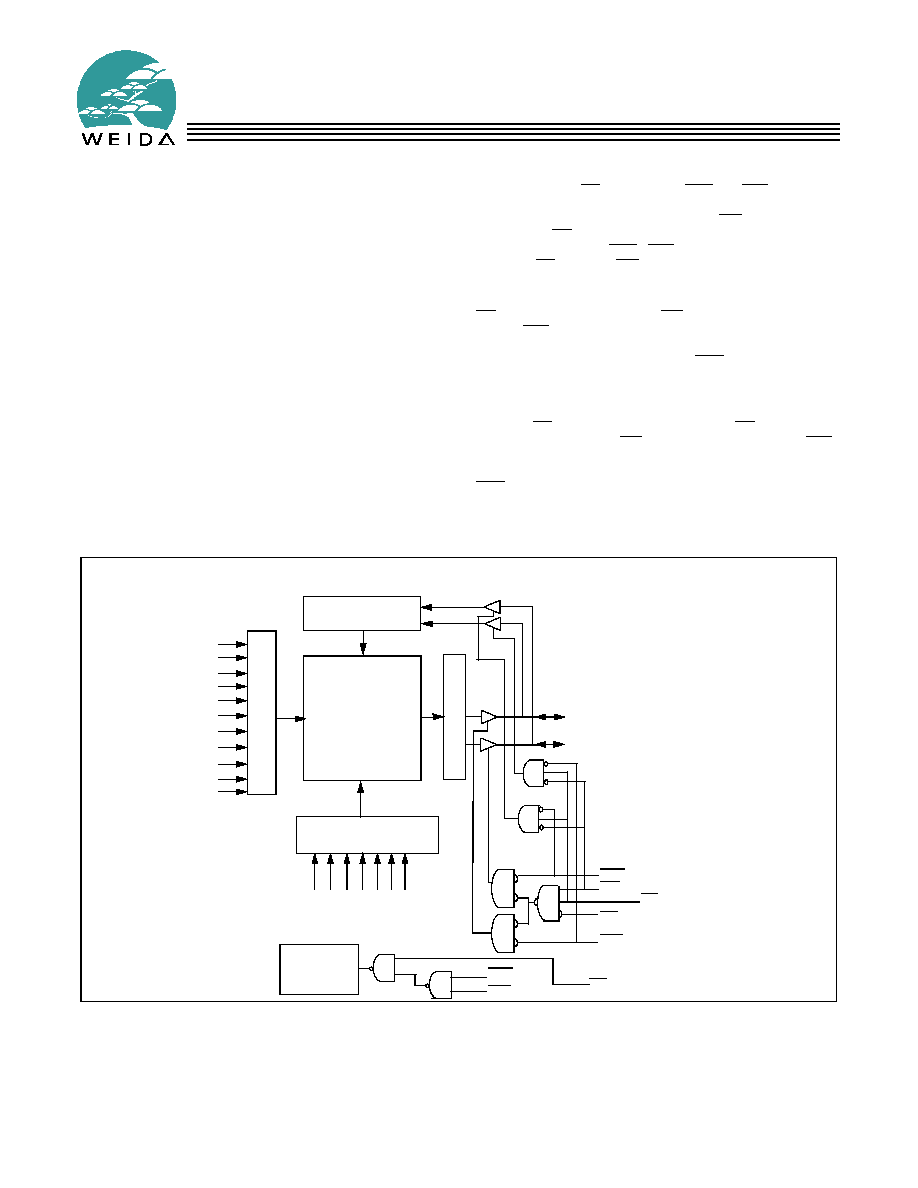
Logic Block Diagram
256K ◊ 16
RAM Array
I/O0 ≠ I/O7
ROW DECODER
A
8
A
7
A
6
A
5
A
2
COLUMN DECODER
A
11
A
12
A
13
A
14
A
15
SENSE AM
PS
DATA IN DRIVERS
OE
A
4
A
3
I/O8 ≠ I/O15
WE
BLE
BHE
A
16
A
0
A
1
A
17
A
9
A
10
Power- Down
Circuit
BHE
BLE
CE
CE
PRELIMINARY
CG6257AM
38-XXXXX
Page - 3 - of 12
Maximum Ratings
(Above which the useful life may be impaired. For user guide-
lines, not tested.)
Storage Temperature ................................≠65∞C to + 150∞C
Ambient Temperature with
Power Applied............................................≠55∞C to + 125∞C
Supply Voltage to Ground Potential................. ≠0.4V to 4.6V
DC Voltage Applied to Outputs
in High Z State
[5, 6, 7]
........................................≠0.4V to 3.3V
DC Input Voltage
[5, 6, 7]
.....................................≠0.4V to 3.3V
Output Current into Outputs (LOW)............................. 20 mA
Static Discharge Voltage .......................................... >2001V
(per MIL-STD-883, Method 3015)
Latch-Up Current .....................................................>200 mA
Operating Range
[9]
Device
Range
Ambient Temperature
V
CC
CG6257AM
Industrial
≠25∞C to +85∞C
2.70V to 3.30V
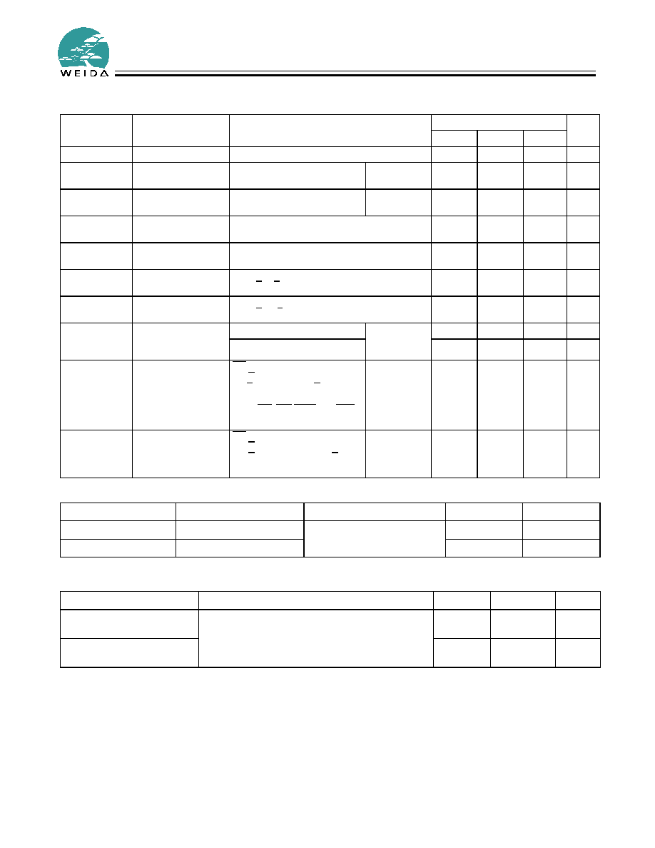
Product Portfolio
Product
V
CC
Range (V)
Speed
(ns)
Power Dissipation
Operating I
CC
(mA)
Standby I
SB2
(
µ
A)
f = 1MHz
f = f
max
Min.
Typ.
[8]
Max.
Typ.
[8]
Max.
Typ.
[8]
Max.
Typ.
[8]
Max.
CG6257AM
2.70
3.0
3.30
70
2
4
13
17
55
80
Notes:
5.
V
IL(MIN)
= -0.5V for pulse durations less than 20ns.
6.
V
IH(Max)
= Vcc + 0.5V for pulse durations less than 20ns.
7.
Overshoot and undershoot specifications are characterized and are not 100% tested.
8.
Typical values are included for reference only and are not guaranteed or tested. Typical values are measured at V
CC
= V
CC(typ.)
, T
A
= 25∞C.
9.
Vcc must be at minimal operational levels before inputs are turned ON.
PRELIMINARY
CG6257AM
38-XXXXX
Page - 4 - of 12
Thermal Resistance
[10]
Electrical Characteristics
Over the Operating Range
Parameter
Description
Test Conditions
CG6257AM-70
Unit
Min.
Typ.
[8]
Max.
V
CC
Supplay Voltage
2.7
3.3
V
V
OH
Output HIGH Voltage I
OH
= ≠1.0 mA
V
CC
= 2.70V
2.4
V
V
OL
Output LOW Voltage I
OL
= 2.0mA
V
CC
= 2.70V
0.4
V
V
IH
Input HIGH Voltage
V
CC
= 2.7V to 3.3V
0.8*Vcc
V
CC
+0.3V
V
V
IL
Input LOW Voltage
V
CC
= 2.7V to 3.3V(F = 0)
-0.3
0.4
V
I
IX
Input Leakage
Current
GND < V
I
< V
CC
≠1
+1
µ
A
I
OZ
Output Leakage
Current
GND < V
O
< V
CC
, Output Disabled
≠1
+1
µ
A
I
CC
V
CC
Operating Supply
Current
f = f
MAX
= 1/t
RC
V
CC
= V
CCmax
I
OUT
= 0 mA
CMOS levels
13
17
mA
f = 1 MHz
2.0
4
mA
I
SB1
Automatic CE
Power-Down
Current -- CMOS
Inputs
CE > V
CC
-
0.2V
V
IN
>V
CC
≠0.2V, V
IN
<0.2V)
f = f
MAX
(Address and Data
Only),
f = 0 (OE, WE, BHE and BLE),
V
CC
=3.30V
Vcc = 3.3V
350
µ
A
I
SB2
Automatic CE
Power-Down
Current -- CMOS
Inputs
CE > V
CC
≠ 0.2V
V
IN
> V
CC
≠ 0.2V or V
IN
< 0.2V,
f = 0, V
CC
= 3.30V
Vcc = 3.3V
55
80
µ
A
Capacitance
[10]
Parameter
Description
Test Conditions
Max.
Unit
C
IN
Input Capacitance
T
A
= 25∞C, f = 1 MHz,
V
CC
= V
CC(typ)
6
pF
C
OUT
Output Capacitance
8
pF
Description
Test Conditions
Symbol
BGA
Unit
Thermal Resistance
(Junction to Ambient)
Still Air, soldered on a 3 ◊ 4.5 inch, two-layer printed
circuit board
JA
55
∞
C/W
Thermal Resistance
(Junction to Case)
JC
16
∞
C/W
Note:
10. Tested initially and after any design or process changes that may affect these parameters.