
32K x 8 Static RAM
WCFS0808C1E
Revised February 18, 2002
S0808C1E
Features
∑ High speed
-- 12 ns
∑ Fast t
DOE
∑ CMOS for optimum speed/power
∑ Easy memory expansion with CE and OE features
∑ TTL-compatible inputs and outputs
∑ Automatic power-down when deselected
Functional Description
The WCFS0808C1E is a high-performance CMOS static RAM
organized as 32K words by 8 bits. Easy memory expansion is
provided by an active LOW Chip Enable (CE) and active LOW
Output Enable (OE) and three-state drivers. This device has
an automatic power-down feature, reducing the power con-
sumption by 81% when deselected. The WCFS0808C1E is in
the standard SOJ package.
An active LOW Write Enable signal (WE) controls the writ-
ing/reading operation of the memory. When CE and WE inputs
are both LOW, data on the eight data input/output pins (I/O
0
through I/O
7
) is written into the memory location addressed by
the address present on the address pins (A
0
through A
14
).
Reading the device is accomplished by selecting the device
and enabling the outputs, CE and OE active LOW, while WE
remains inactive or HIGH. Under these conditions, the con-
tents of the location addressed by the information on address
pins are present on the eight data input/output pins.
The input/output pins remain in a high-impedance state unless
the chip is selected, outputs are enabled, and Write Enable
(WE) is HIGH. A die coat is used to improve alpha immunity.
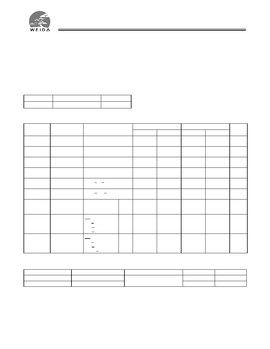
Selection Guide
WCFS0808C1E 12ns
WCFS0808C1E 15ns
Maximum Access Time (ns)
12
15
Maximum Operating Current (mA)
160
155
Maximum CMOS Standby Current (mA)
10
10
Logic Block Diagram
Pin Configurations
A
1
A
2
A
3
A
4
A
5
A
6
A
7
A
8
COLUMN
DECODER
RO
W DE
C
O
D
E
R
SE
N
S
E A
M
P
S
INPUT BUFFER
POWER
DOWN
WE
OE
I/O
0
CE
I/O
1
I/O
2
I/O
3
1
2
3
4
5
6
7
8
9
10
11
14
15
16
20
19
18
17
21
24
23
22
Top View
SOJ
12
13
25
28
27
26
GND
A
6
A
7
A
8
A
9
A
10
A
11
A
12
A
13
WE
V
CC
A
4
A
3
A
2
A
1
I/O
7
I/O
6
I/O
5
I/O
4
A
14
A
5
I/O
0
I/O
1
I/O
2
CE
OE
A
0
I/O
3
1024 x 32 x 8
ARRAY
I/O
7
I/O
6
I/O
5
I/O
4
A
9
A
0
A
11
A
13
A
12
A
14
A
10
WCFS0808C1E
Page 2 of 10
Maximum Ratings
(Above which the useful life may be impaired. For user guide-
lines, not tested.)
Storage Temperature ................................. ≠65
∞
C to +150
∞
C
Ambient Temperature with
Power Applied............................................. ≠55
∞
C to +125
∞
C
Supply Voltage to Ground Potential
(Pin 28 to Pin 14) ........................................... ≠0.5V to +7.0V
DC Voltage Applied to Outputs
in High Z State
[1]
.................................... ≠0.5V to V
CC
+ 0.5V
DC Input Voltage
[1]
................................ ≠0.5V to V
CC
+ 0.5V
Output Current into Outputs (LOW)............................. 20 mA
Static Discharge Voltage........................................... >2001V
(per MIL-STD-883, Method 3015)
Latch-Up Current .................................................... >200 mA
]
Operating Range
Range
Ambient Temperature
[2]
V
CC
Commercial
0
∞
C to +70
∞
C
5V
±
10%
Electrical Characteristics
Over the Operating Range
[3]
WCFS0808C1E 12ns
WCFS0808C1E 15ns
Parameter
Description
Test Conditions
Min.
Max.
Min.
Max.
Unit
V
OH
Output HIGH
Voltage
V
CC
= Min., I
OH
=≠4.0 mA
2.4
2.4
V
V
OL
Output LOW
Voltage
V
CC
= Min., I
OL
=8.0 mA
0.4
0.4
V
V
IH
Input HIGH
Voltage
2.2
V
CC
+0.3V
2.2
V
CC
+0.3V
V
V
IL
Input LOW
Voltage
≠0.5
0.8
≠0.5
0.8
V
I
IX
Input Load
Current
GND < V
I
< V
CC
≠5
+5
≠5
+5
µ
A
I
OZ
Output Leakage
Current
GND < V
O
< V
CC
,
Output Disabled
≠5
+5
≠5
+5
µ
A
I
CC
V
CC
Operating
Supply Current
V
CC
= Max.,
I
OUT
= 0 mA,
f = f
MAX
= 1/t
RC
Com'l
160
155
mA
I
SB1
Automatic CE
Power-Down
Current-- TTL
Inputs
Max. V
CC
,
CE > V
IH
,
V
IN
> V
IH
or
V
IN
< V
IL
, f = f
MAX
Com'l
30
30
mA
I
SB2
Automatic CE
Power-Down
Current-- CMOS
Inputs
Max. V
CC
,
CE > V
CC
≠ 0.3V
V
IN
> V
CC
≠ 0.3V
or V
IN
< 0.3V, f = 0
Com'l
10
10
mA
Capacitance
[1]
Parameter
Description
Test Conditions
Max.
Unit
C
IN
Input Capacitance
T
A
= 25
∞
C, f = 1 MHz,
V
CC
= 5.0V
8
pF
C
OUT
Output Capacitance
8
pF
Notes:
1.
V
IL
(min.)
= ≠2.0V for pulse durations of less than 20 ns.
2.
T
A
is the "instant on" case temperature.
3.
See the last page of this specification for Group A subgroup testing information.
4.
Tested initially and after any design or process changes that may affect these parameters.

WCFS0808C1E
Page 3 of 10
AC Test Loads and Waveforms
[5]
Data Retention Characteristics (
Over the Operating Range)
Parameter
Description
Conditions
[6]
Min.
Max.
Unit
V
DR
V
CC
for Data Retention
2.0
V
t
CDR
[1]
Chip Deselect to Data Retention Time V
CC
= V
DR
= 2.0V,
CE > V
CC
≠ 0.3V,
V
IN
> V
CC
≠ 0.3V or
V
IN
< 0.3V
0
ns
t
R
[5]
Operation Recovery Time
200
µ
s
Data Retention Waveform
Note:
5.
t
R
< 3 ns for the -12 and the -15 speeds. t
R
< 5 ns for the -20 and slower speeds
6.
No input may exceed V
CC
+ 0.5V.
3.0V
5V
OUTPUT
R1 481
R2
255
30 pF
INCLUDING
JIG AND
SCOPE
GND
90%
10%
90%
10%
t
r
t
r
5V
OUTPUT
R1 481
R2
255
5 pF
INCLUDING
JIG AND
SCOPE
(a)
(b)
OUTPUT
1.73V
Equivalent to:
TH… VENIN EQUIVALENT
ALL INPUT PULSES
C199≠5
167
3.0V
3.0V
t
CDR
V
DR
> 2V
DATA RETENTION MODE
t
R
CE
V
CC

WCFS0808C1E
Page 4 of 10
Switching Characteristics
Over the Operating Range
[3, 7]
WCFS0808C1E 12ns
WCFS0808C1E 15ns
Unit
Parameter
Description
Min.
Max.
Min.
Max.
READ CYCLE
t
RC
Read Cycle Time
12
15
ns
t
AA
Address to Data Valid
12
15
ns
t
OHA
Data Hold from Address Change
3
3
ns
t
ACE
CE LOW to Data Valid
12
15
ns
t
DOE
OE LOW to Data Valid
5
7
ns
t
LZOE
OE LOW to Low Z
[8]
0
0
ns
t
HZOE
OE HIGH to High Z
[8, 9]
5
7
ns
t
LZCE
CE LOW to Low Z
[8]
3
3
ns
t
HZCE
CE HIGH to High Z
[8,9]
5
7
ns
t
PU
CE LOW to Power-Up
0
0
ns
t
PD
CE HIGH to Power-Down
12
15
ns
WRITE CYCLE
[10, 11]
t
WC
Write Cycle Time
12
15
ns
t
SCE
CE LOW to Write End
9
10
ns
t
AW
Address Set-Up to Write End
9
10
ns
t
HA
Address Hold from Write End
0
0
ns
t
SA
Address Set-Up to Write Start
0
0
ns
t
PWE
WE Pulse Width
8
9
ns
t
SD
Data Set-Up to Write End
8
9
ns
t
HD
Data Hold from Write End
0
0
ns
t
HZWE
WE LOW to High Z
[9]
7
7
ns
t
LZWE
WE HIGH to Low Z
[8]
3
3
ns
Notes:
7.
Test conditions assume signal transition time of 3 ns or less for -12 and -15 speeds and 5 ns or less for -20 and slower speeds, timing reference levels
of 1.5V, input pulse levels of 0 to 3.0V, and output loading of the specified I
OL
/I
OH
and 30-pF load capacitance.
8.
At any given temperature and voltage condition, t
HZCE
is less than t
LZCE
, t
HZOE
is less than t
LZOE
, and t
HZWE
is less than t
LZWE
for any given device.
9.
t
HZOE
, t
HZCE
, and t
HZWE
are specified with C
L
= 5 pF as in part (b) of AC Test Loads. Transition is measured
±
500 mV from steady-state voltage.
10. The internal write time of the memory is defined by the overlap of CE LOW and WE LOW. Both signals must be LOW to initiate a write and either signal can
terminate a write by going HIGH. The data input set-up and hold timing should be referenced to the rising edge of the signal that terminates the write.
11. The minimum write cycle time for write cycle #3 (WE controlled, OE LOW) is the sum of t
HZWE
and t
SD
.
WCFS0808C1E
Page 5 of 10
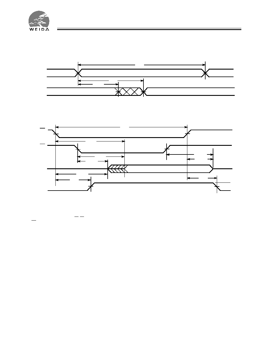
Read Cycle No. 1
[12, 13]
Read Cycle No. 2
[13, 14]
Notes:
12. Device is continuously selected. OE, CE = V
IL
13. .WE is HIGH for read cycle
ADDRESS
DATA OUT
PREVIOUS DATA VALID
DATA VALID
t
RC
t
AA
t
OHA
50%
50%
DATA VALID
t
RC
t
ACE
t
DOE
t
LZOE
t
LZCE
t
PU
DATA OUT
HIGH IMPEDANCE
IMPEDANCE
ICC
ISB
t
HZOE
t
HZCE
t
PD
OE
CE
HIGH
V
CC
SUPPLY
CURRENT

WCFS0808C1E
Page 6 of 10
Write Cycle No. 1 (WE Controlled)
[10, 15, 16]
Write Cycle No. 2 (CE Controlled)
[10, 15, 16]
Notes:
14. Address valid prior to or coincident with CE transition LOW.
15. Data I/O is high impedance if OE = V
IH
.
16. If CE goes HIGH simultaneously with WE HIGH, the output remains in a high-impedance state.
t
HD
t
SD
t
PWE
t
SA
t
HA
t
AW
t
WC
DATA I/O
ADDRESS
CE
WE
OE
t
HZOE
DATA
IN
VALID
t
WC
t
AW
t
SA
t
HA
t
HD
t
SD
t
SCE
WE
DATA I/O
ADDRESS
CE
DATA
IN
VALID

WCFS0808C1E
Page 7 of 10
Write Cycle No. 3 (WE Controlled OE LOW)
[11, 16]
Typical DC and AC Characteristics
DATA I/O
ADDRESS
t
HD
t
SD
t
LZWE
t
SA
t
HA
t
AW
t
WC
CE
WE
t
HZWE
DATA
IN
VALID
1.2
1.4
1.0
0.6
0.4
0.2
4.0
4.5
5.0
5.5
6.0
1.6
1.4
1.2
1.0
0.8
≠55
25
125
≠55
25
125
1.2
1.0
0.8
NORMA
L
I
Z
E
D
t
AA
120
100
80
60
40
20
0.0
1.0
2.0
3.0
4.0
OUT
P
UT S
O
URCE
CURRE
NT (m
A
)
SUPPLY VOLTAGE (V)
NORMALIZED SUPPLY CURRENT
vs. SUPPLY VOLTAGE
NORMALIZED ACCESS TIME
vs. AMBIENT TEMPERATURE
AMBIENT TEMPERATURE (
∞
C)
NORMALIZED SUPPLY CURRENT
vs. AMBIENT TEMPERATURE
AMBIENT TEMPERATURE (
∞
C)
OUTPUT VOLTAGE (V)
OUTPUT SOURCE CURRENT
vs. OUTPUT VOLTAGE
0.0
0.8
1.4
1.1
1.0
0.9
4.0
4.5
5.0
5.5
6.0
NORMA
L
I
Z
E
D
t
SUPPLY VOLTAGE (V)
NORMALIZED ACCESS TIME
vs. SUPPLY VOLTAGE
120
140
100
60
40
20
0.0
1.0
2.0
3.0
4.0
O
U
T
P
UT S
I
NK
CURR
E
N
T (m
A
)
0
80
OUTPUT VOLTAGE (V)
OUTPUT SINK CURRENT
vs. OUTPUT VOLTAGE
0.6
0.4
0.2
0.0
NORMA
L
I
Z
E
D
I
CC
,I
SB
NORM
A
L
IZE
D
I
CC
,I
SB
I
SB
I
CC
I
CC
V
CC
=5.0V
V
CC
=5.0V
T
A
=25
∞
C
V
CC
=5.0V
T
A
=25
∞
C
I
SB
T
A
=25
∞
C
0.6
0.8
0
AA
1.3
1.2
V
IN
=5.0V
T
A
=25
∞
C
1.4
V
CC
=5.0V
V
IN
=5.0V

WCFS0808C1E
Page 8 of 10
Truth Table
CE
WE
OE
Inputs/Outputs
Mode
Power
H
X
X
High Z
Deselect/Power-Down
Standby (I
SB
)
L
H
L
Data Out
Read
Active (I
CC
)
L
L
X
Data In
Write
Active (I
CC
)
L
H
H
High Z
Deselect, Output Disabled
Active (I
CC
)
Ordering Information
Speed
(ns)
Ordering Code
Package
Name
Package Type
Operating
Range
12
WCFS0808C1E-JC12
J
28-Lead Molded SOJ
Commercial
15
WCFS0808C1E-JC15
J
28-Lead Molded SOJ
Typical DC and AC Characteristics
(continued)
3.0
2.5
2.0
1.5
1.0
0.5
0.0
1.0
2.0
3.0
4.0
NORMA
L
I
Z
E
D
I
PO
SUPPLY VOLTAGE (V)
TYPICAL POWER-ON CURRENT
vs. SUPPLY VOLTAGE
30.0
25.0
20.0
15.0
10.0
5.0
0
200
400
600
800
DE
L
T
A t
(
n
s
)
AA
CAPACITANCE (pF)
TYPICAL ACCESS TIME CHANGE
vs. OUTPUT LOADING
1.25
1.00
0.75
10
20
30
40
NORMA
L
I
Z
E
D
I
CC
CYCLE FREQUENCY (MHz)
NORMALIZED I
CC
vs. CYCLE TIME
0.0
5.0
0.0
1000
0.50
V
CC
=4.5V
T
A
=25
∞
C
V
CC
=5.0V
T
A
=25
∞
C
V
IN
=0.5V

WCFS0808C1E
Page 9 of 10
Package Diagrams
28-Lead (300-Mil) Molded SOJ,J

WCFS0808C1E
Page 10 of 10
Document Title: WCFS0808C1E 32K x 8 Static RAM
REV.
Issue Date
Orig. of Change
Description of Change
**
4/16/2002
XFL
New Datasheet