32K x 8 3.3V Static RAM
WCFS0808V1E
Document #: 38-05225 Rev. **
Revised February 11, 2002
1WCFS0808V1E
Features
∑ Single 3.3V power supply
∑ Ideal for low-voltage cache memory applications
∑ High speed
-- 12/15 ns
∑ Plastic SOJ and TSOP packaging
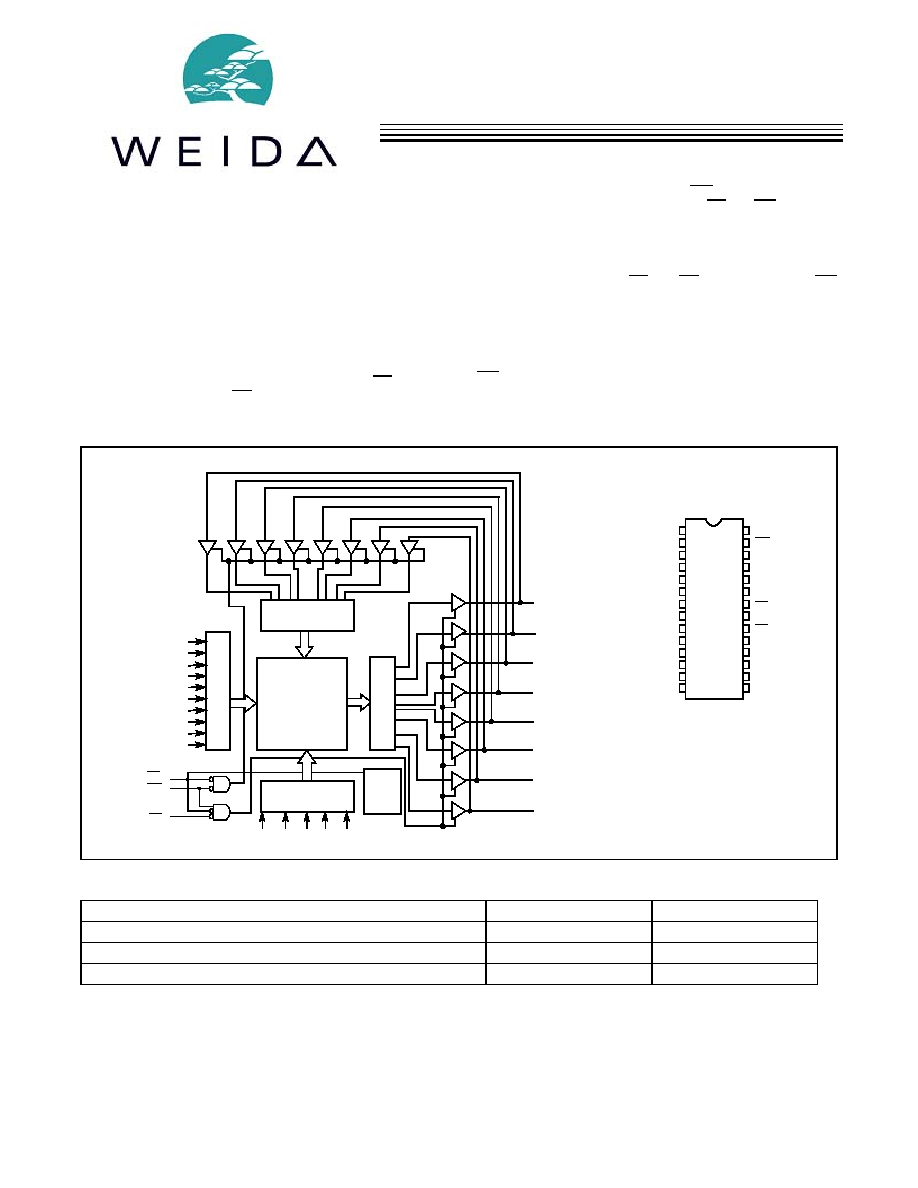
Functional Description
The WCFS0808V1E is a high-performance 3.3V CMOS Static
RAM organized as 32K words by 8 bits. Easy memory expan-
sion is provided by an active LOW Chip Enable (CE) and ac-
tive LOW Output Enable (OE) and three-state drivers. The de-
vice has an automatic power-down feature, reducing the
power consumption by more than 95% when deselected.
An active LOW Write Enable signal (WE) controls the writing/
reading operation of the memory. When CE and WE inputs are
both LOW, data on the eight data input/output pins (I/O
0
through I/O
7
) is written into the memory location addressed by
the address present on the address pins (A
0
through A
14
).
Reading the device is accomplished by selecting the device
and enabling the outputs, CE and OE active LOW, while WE
remains inactive or HIGH. Under these conditions, the con-
tents of the location addressed by the information on address
pins is present on the eight data input/output pins.
The input/output pins remain in a high-impedance state unless
the chip is selected, outputs are enabled, and Write Enable
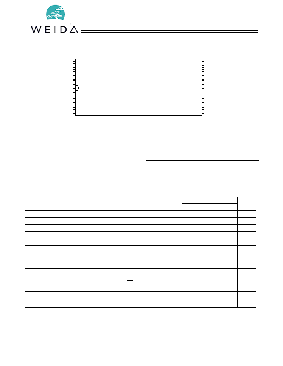
(WE) is HIGH. The WCFS0808V1E is available in 28-pin stan-
dard 300-mil-wide SOJ and TSOP Type I packages.
Logic Block Diagram
Pin Configurations
1
2
3
4
5
6
7
8
9
10
11
14
15
16
20
19
18
17
21
24
23
22
Top View
SOJ
12
13
25
28
27
26
GND
A
6
A
7
A
8
A
9
A
10
A
11
A
12
A
13
WE
V
CC
A
4
A
3
A
2
A
1
I/O
7
I/O
6
I/O
5
I/O
4
A
14
A
5
I/O
0
I/O
1
I/O
2
CE
OE
A
0
I/O
3
A
1
A
2
A
3
A
4
A
5
A
6
A
7
A
8
COLUMN
DECODER
ROW DE
CODE
R
SE
N
SE A
M
PS
INPUT BUFFER
POWER
DOWN
WE
OE
I/O
0
CE
I/O
1
I/O
2
I/O
3
32K x 8
ARRAY
I/O
7
I/O
6
I/O
5
I/O
4
A
9
A
0
A
11
A
13
A
12
A
14
A
10
Selection Guide
WCFS0808V1E 12ns
WCFS0808V1E 15ns
Maximum Access Time (ns)
12
15
Maximum Operating Current (mA)
55
50
Maximum CMOS Standby Current (
µA)
500
500
WCFS0808V1E
Document #: 38-05225 Rev. **
Page 2 of 10
Maximum Ratings
(Above which the useful life may be impaired. For user guide-
lines, not tested.)
Storage Temperature ................................. ≠65
∞C to +150∞C
Ambient Temperature with
Power Applied............................................. ≠55
∞C to +125∞C
Supply Voltage on V
CC
to Relative GND
[1]
.... ≠0.5V to +4.6V
DC Voltage Applied to Outputs
in High Z State
[1]
....................................≠0.5V to V
CC
+ 0.5V
DC Input Voltage
[1]
.................................≠0.5V to V
CC
+ 0.5V
Output Current into Outputs (LOW)............................. 20 mA
Static Discharge Voltage........................................... >2001V
(per MIL-STD-883, Method 3015)
Latch-Up Current.................................................... >200 mA
Pin Configuration
22
23
24
25
26
27
28
1
2
5
10
11
15
14
13
12
16
19
18
17
Top View
TSOP
3
4
20
21
7
6
8
9
OE
A
1
A
2
A
3
A
4
WE
V
CC
A
5
A
6
A
7
A
8
A
9
A
0
CE
I/O
7
I/O
6
I/O
5
GND
I/O
2
I/O
1
I/O
4
I/O
0
A
14
A
10
A
11
A
13
A
12
I/O
3
Operating Range
Range
Ambient
Temperature
V
CC
Commercial
0
∞
C to +70
∞
C
3.3V
±300 mV
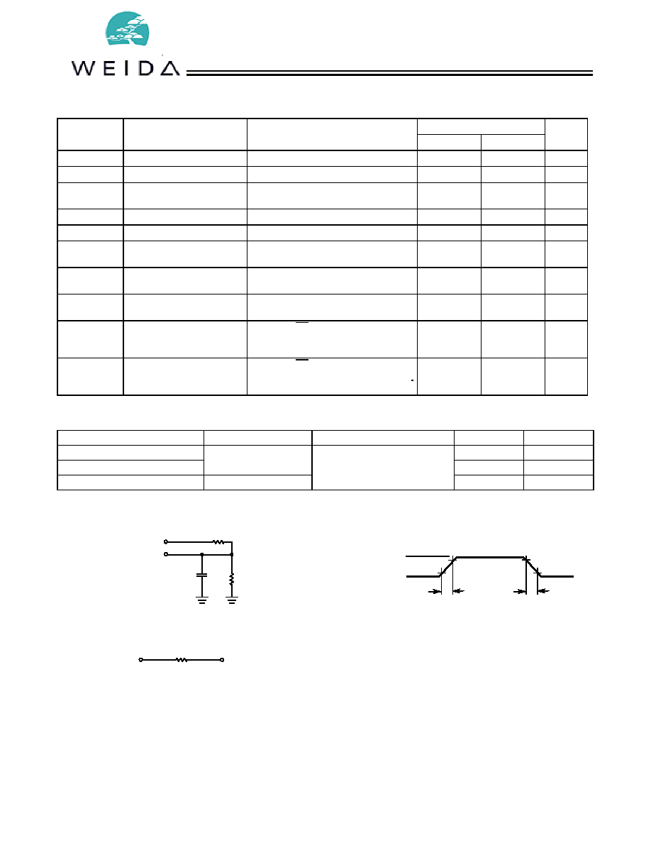
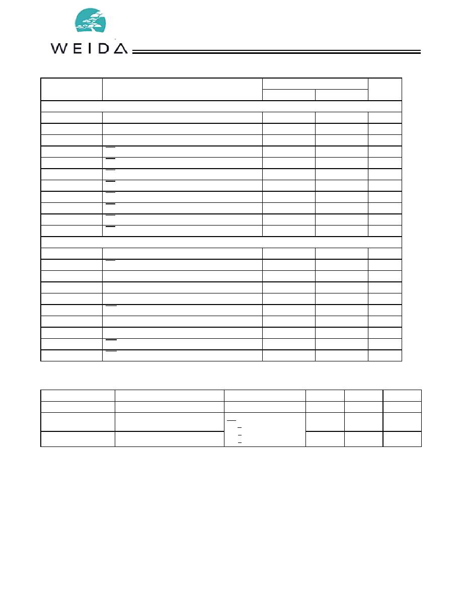
Electrical Characteristics
Over the Operating Range
[1]
WCFS0808V1E 12ns
Parameter
Description
Test Conditions
Min.
Max.
Unit
V
OH
Output HIGH Voltage
V
CC
= Min., I
OH
= ≠2.0 mA
2.4
V
V
OL
Output LOW Voltage
V
CC
= Min., I
OL
= 4.0 mA
0.4
V
V
IH
Input HIGH Voltage
2.2
V
CC
+0.3V
V
V
IL
Input LOW Voltage
≠0.3
0.8
V
I
IX
Input Load Current
≠1
+1
µA
I
OZ
Output Leakage
Current
GND
V
I
V
CC
,
Output Disabled
≠5
+5
µA
I
OS
Output Short
Circuit Current
[2]
V
CC
= Max., V
OUT
= GND
≠300
mA
I
CC
V
CC
Operating
Supply Current
V
CC
= Max., I
OUT
= 0 mA,
f = f
MAX
= 1/t
RC
55
mA
I
SB1
Automatic CE Power-Down
Current -- TTL Inputs
Max. V
CC
, CE
V
IH
,
V
IN
V
IH
, or V
IN
V
IL
,f = f
MAX
5
mA
I
SB2
Automatic CE Power-Down
Current -- CMOS Inputs
[3]
Max. V
CC
, CE
V
CC
≠ 0.3V, V
IN
V
CC
≠
0.3V, or V
IN
0.3V,
WE
V
CC
≠ 0.3V or WE
0.3V, f = f
MAX
500
µA
Notes:
1.
Minimum voltage is equal to ≠ 2.0V for pulse durations of less than 20 ns.
2.
Not more than one output should be shorted at one time. Duration of the short circuit should not exceed 30 seconds.
3.
Device draws low standby current regardless of switching on the addresses.
WCFS0808V1E
Document #: 38-05225 Rev. **
Page 3 of 10
Electrical Characteristics
Over the Operating Range (continued)
WCFS0808V1E 15ns
Parameter
Description
Test Conditions
Min.
Max.
Unit
V
OH
Output HIGH Voltage
V
CC
= Min., I
OH
= ≠2.0 mA
2.4
V
V
OL
Output LOW Voltage
V
CC
= Min., I
OL
= 4.0 mA
0.4
V
V
IH
Input HIGH Voltage
2.2
V
CC
+0.3V
V
V
IL
Input LOW Voltage
≠0.3
0.8
V
I
IX
Input Load Current
≠1
+1
µA
I
OZ
Output Leakage Current
GND
V
I
V
CC
,
Output Disabled
≠5
+5
µA
I
OS
Output Short Circuit
Current
[2]
V
CC
= Max., V
OUT
= GND
≠300
mA
I
CC
V
CC
Operating
Supply Current
V
CC
= Max., I
OUT
= 0 mA,
f = f
MAX
= 1/t
RC
50
mA
I
SB1
Automatic CE Power-Down
Current -- TTL Inputs
Max. V
CC
, CE
V
IH
,
V
IN
V
IH
, or V
IN
V
IL
,
f = f
MAX
5
mA
I
SB2
Automatic CE Power-Down
Current -- CMOS Inputs
[3]
Max. V
CC
, CE
V
CC
≠0.3V, V
IN
V
CC
≠
0.3V, or V
IN
0.3V, WEV
CC
≠0.3V or WE
0.3V, f=f
MAX
500
µA
Capacitance
[4]
Parameter
Description
Test Conditions
Max.
Unit
C
IN
: Addresses
Input Capacitance
T
A
= 25
∞C, f = 1 MHz, V
CC
= 3.3V
5
pF
C
IN
: Controls
6
pF
C
OUT
Output Capacitance
6
pF
AC Test Loads and Waveforms
Note:
4.
Tested initially and after any design or process changes that may affect these parameters.
3.0V
3.3V
OUTPUT
R1 317
R2
351
C
L
INCLUDING
JIG AND
SCOPE
GND
90%
10%
90%
10%
3 ns
3 ns
OUTPUT
1.73V
Equivalent to:
TH…VENIN EQUIVALENT
ALL INPUT PULSES
167
WCFS0808V1E
Document #: 38-05225 Rev. **
Page 4 of 10
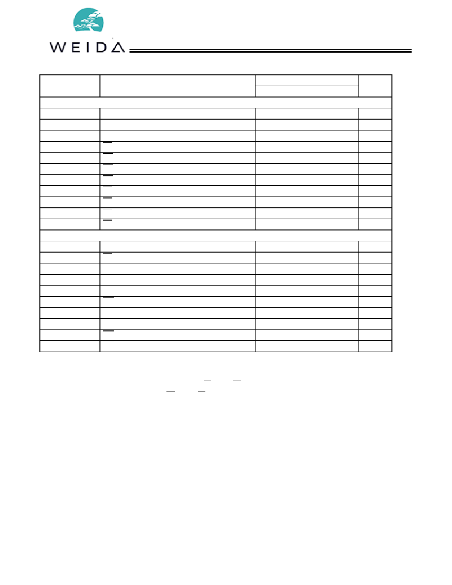
Switching Characteristics
Over the Operating Range
[5]
WCFS0808V1E 12ns
Parameter
Description
Min.
Max.
Unit
READ CYCLE
t
RC
Read Cycle Time
12
ns
t
AA
Address to Data Valid
12
ns
t
OHA
Data Hold from Address Change
3
ns
t
ACE
CE LOW to Data Valid
12
ns
t
DOE
OE LOW to Data Valid
5
ns
t
LZOE
OE LOW to Low Z
[6]
0
ns
t
HZOE
OE HIGH to High Z
[6, 7]
5
ns
t
LZCE
CE LOW to Low Z
[6]
3
ns
t
HZCE
CE HIGH to High Z
[6, 7]
6
ns
t
PU
CE LOW to Power-Up
0
ns
t
PD
CE HIGH to Power-Down
12
ns
WRITE CYCLE
[8, 9]
t
WC
Write Cycle Time
12
ns
t
SCE
CE LOW to Write End
8
ns
t
AW
Address Set-Up to Write End
8
ns
t
HA
Address Hold from Write End
0
ns
t
SA
Address Set-Up to Write Start
0
ns
t
PWE
WE Pulse Width
8
ns
t
SD
Data Set-Up to Write End
7
ns
t
HD
Data Hold from Write End
0
ns
t
HZWE
WE LOW to High Z
[8]
7
ns
t
LZWE
WE HIGH to Low Z
[6]
3
ns
Notes:
5.
Test conditions assume signal transition time of 3 ns or less, timing reference levels of 1.5V, input pulse levels of 0 to 3.0V, and output loading of the
specified I
OL
/I
OH
and capacitance C
L
= 30 pF.
6.
At any given temperature and voltage condition, t
HZCE
is less than t
LZCE
, t
HZOE
is less than t
LZOE
, and t
HZWE
is less than t
LZWE
for any given device.
7.
t
HZOE
, t
HZCE
, t
HZWE
are specified with C
L
= 5 pF as in AC Test Loads. Transition is measured ±500 mV from steady state voltage.
8.
The internal write time of the memory is defined by the overlap of CE LOW and WE LOW. Both signals must be LOW to initiate a write and either signal can
terminate a write by going HIGH. The data input set-up and hold timing should be referenced to the rising edge of the signal that terminates the write.
9.
The minimum write cycle time for write cycle #3 (WE controlled, OE LOW) is the sum of t
HZWE
and t
SD
.
WCFS0808V1E
Document #: 38-05225 Rev. **
Page 5 of 10
Switching Characteristics
Over the Operating Range
[5]
(Continued)
WCFS0808V1E 15ns
Parameter
Description
Min.
Max.
Unit
READ CYCLE
t
RC
Read Cycle Time
15
ns
t
AA
Address to Data Valid
15
ns
t
OHA
Data Hold from Address Change
3
ns
t
ACE
CE LOW to Data Valid
15
ns
t
DOE
OE LOW to Data Valid
6
ns
t
LZOE
OE LOW to Low Z
[6]
0
ns
t
HZOE
OE HIGH to High Z
[6, 7]
6
ns
t
LZCE
CE LOW to Low Z
[6]
3
ns
t
HZCE
CE HIGH to High Z
[6, 7]
7
ns
t
PU
CE LOW to Power-Up
0
ns
t
PD
CE HIGH to Power-Down
15
ns
WRITE CYCLE
[8, 9]
t
WC
Write Cycle Time
15
ns
t
SCE
CE LOW to Write End
10
ns
t
AW
Address Set-Up to Write End
10
ns
t
HA
Address Hold from Write End
0
ns
t
SA
Address Set-Up to Write Start
0
ns
t
PWE
WE Pulse Width
10
ns
t
SD
Data Set-Up to Write End
8
ns
t
HD
Data Hold from Write End
0
ns
t
HZWE
WE LOW to High Z
[8]
7
ns
t
LZWE
WE HIGH to Low Z
[6]
3
ns
Data Retention Characteristics
(Over the Operating Range)
Parameter
Description
Conditions
Min.
Max.
Unit
V
DR
V
CC
for Data Retention
2.0
V
t
CDR
Chip Deselect to Data
Retention Time
V
CC
= V
DR
= 2.0V,
CE > V
CC
≠ 0.3V,
V
IN
> V
CC
≠ 0.3V or
V
IN
< 0.3V
0
ns
t
R
Operation Recovery Time
t
RC
ns