64K x 16 Static RAM
WCFS1016V1C
Revised April 19, 2002
1021BV33
Features
∑ 3.3V operation (3.0V≠3.6V)
∑ High speed
-- t
AA
= 12 ns
∑ CMOS for optimum speed/power
∑ Automatic power-down when deselected
∑ Independent control of upper and lower bits
∑ Available in 400-mil SOJ
Functional Description
The WCFS1016V1C is a high-performance CMOS static RAM
organized as 65,536 words by 16 bits. This device has an au-
tomatic power-down feature that significantly reduces power
consumption when deselected.
Writing to the device is accomplished by taking Chip Enable
(CE) and Write Enable (WE) inputs LOW. If Byte Low Enable
(BLE) is LOW, then data from I/O pins (I/O
1
through I/O
8
), is
written into the location specified on the address pins (A
0
through A
15
). If Byte High Enable (BHE) is LOW, then data
from I/O pins (I/O
9
through I/O
16
) is written into the location
specified on the address pins (A
0
through A
15
).
Reading from the device is accomplished by taking Chip En-
able (CE) and Output Enable (OE) LOW while forcing the Write
Enable (WE) HIGH. If Byte Low Enable (BLE) is LOW, then
data from the memory location specified by the address pins
will appear on I/O
1
to I/O
8
. If Byte High Enable (BHE) is LOW,
then data from memory will appear on I/O
9
to I/O
16.
See the
truth table at the back of this data sheet for a complete descrip-
tion of read and write modes.
The input/output pins (I/O
1
through I/O
16
) are placed in a
high-impedance state when the device is deselected
(CE HIGH), the outputs are disabled (OE HIGH), the BHE and
BLE are disabled (BHE, BLE HIGH), or during a write opera-
tion (CE LOW, and WE LOW).
The WCFS1016V1C is available in 400-mil-wide SOJ packag-
es.
WE
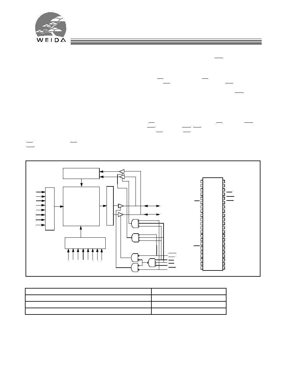
Logic Block Diagram
Pin Configurations
1
2
3
4
5
6
7
8
9
10
11
14
31
32
36
35
34
33
37
40
39
38
Top View
SOJ
12
13
41
44
43
42
16
15
29
30
V
CC
A15
A14
A13
A12
NC
A
4
A3
OE
V
SS
A5
I/O16
A2
CE
I/O3
I/O1
I/O2
BHE
NC
A1
A0
18
17
20
19
I/O4
27
28
25
26
22
21
23
24
NC
V
SS
I/O7
I/O5
I/O6
I/O8
A6
A7
BLE
V
CC
I/O15
I/O14
I/O13
I/O12
I/O11
I/O10
I/O9
A8
A9
A10
A11
64K x 16
RAM Array
I/O
1
≠ I/O
8
ROW
DE
C
O
D
E
R
A
7
A
6
A
5
A
4
A
3
A
0
COLUMN DECODER
A
9
A
10
A
11
A
12
A
13
A
14
A
15
512 X 2048
SEN
SE AM
PS
DATA IN DRIVERS
OE
A
2
A
1
I/O
9
≠ I/O
16
CE
WE
BLE
BHE
A
8
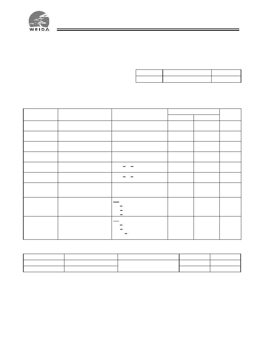
Selection Guide
WCFS1016V1C-12
Maximum Access Time (ns)
12
Maximum Operating Current (mA)
150
Maximum CMOS Standby Current (mA)
5
WCFS1016V1C
Page 2 of 9
Maximum Ratings
(Above which the useful life may be impaired. For user guide-
lines, not tested.)
Storage Temperature ................................. ≠65∞C to +150∞C
Ambient Temperature with
Power Applied............................................. ≠55∞C to +125∞C
Supply Voltage on V
CC
to Relative GND
[1]
.... ≠0.5V to +4.6V
DC Voltage Applied to Outputs
in High Z State
[1]
......................................≠0.5V to V
CC
+0.5V
DC Input Voltage
[1]
...................................≠0.5V to V
CC
+0.5V
Current into Outputs (LOW) ........................................ 20 mA
Static Discharge Voltage............................................ >2001V
(per MIL-STD-883, Method 3015)
Latch-Up Current ..................................................... >200 mA
Operating Range
Range
Ambient Temperature
[2]
V
CC
Commercial
0∞C to +70∞C
3.3V
±
10%
Electrical Characteristics
Over the Operating Range
Parameter
Description
Test Conditions
WCFS1016V1C 12ns
Unit
Min.
Max.
V
OH
Output HIGH
Voltage
V
CC
= Min.,
I
OH
= ≠4.0 mA
2.4
V
V
OL
Output LOW
Voltage
V
CC
= Min., I
OL
= 8.0 mA
0.4
V
V
IH
Input HIGH
Voltage
2.2
V
CC
+ 0.3V
V
V
IL
Input LOW
Voltage
[1]
≠0.3
0.8
V
I
IX
Input Load
Current
GND < V
I
< V
CC
≠1
+1
µ
A
I
OZ
Output Leakage
Current
GND < V
I
< V
CC
,
Output Disabled
≠1
+1
µ
A
I
CC
V
CC
Operating
Supply Current
V
CC
= Max.,
I
OUT
= 0 mA,
f = f
MAX
= 1/t
RC
150
mA
I
SB1
Automatic CE
Power-Down
Current
--TTL Inputs
Max. V
CC
,
CE > V
IH
V
IN
> V
IH
or
V
IN
< V
IL
, f = f
MAX
40
mA
I
SB2
Automatic CE
Power-Down
Current
--CMOS Inputs
Max. V
CC
,
CE > V
CC
≠ 0.3V,
V
IN
> V
CC
≠ 0.3V,
or V
IN
< 0.3V,
f = 0
5
mA
Capacitance
[3]
Parameter
Description
Test Conditions
Max.
Unit
C
IN
Input Capacitance
T
A
= 25∞C, f = 1 MHz
6
pF
C
OUT
Output Capacitance
8
pF
Note:
1.
V
IL
(min.) = ≠2.0V for pulse durations of less than 20 ns.
2.
T
A
is the "instant on" case temperature.
3.
Tested initially and after any design or process changes that may affect these parameters.
WCFS1016V1C
Page 3 of 9
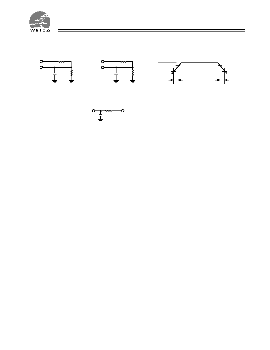
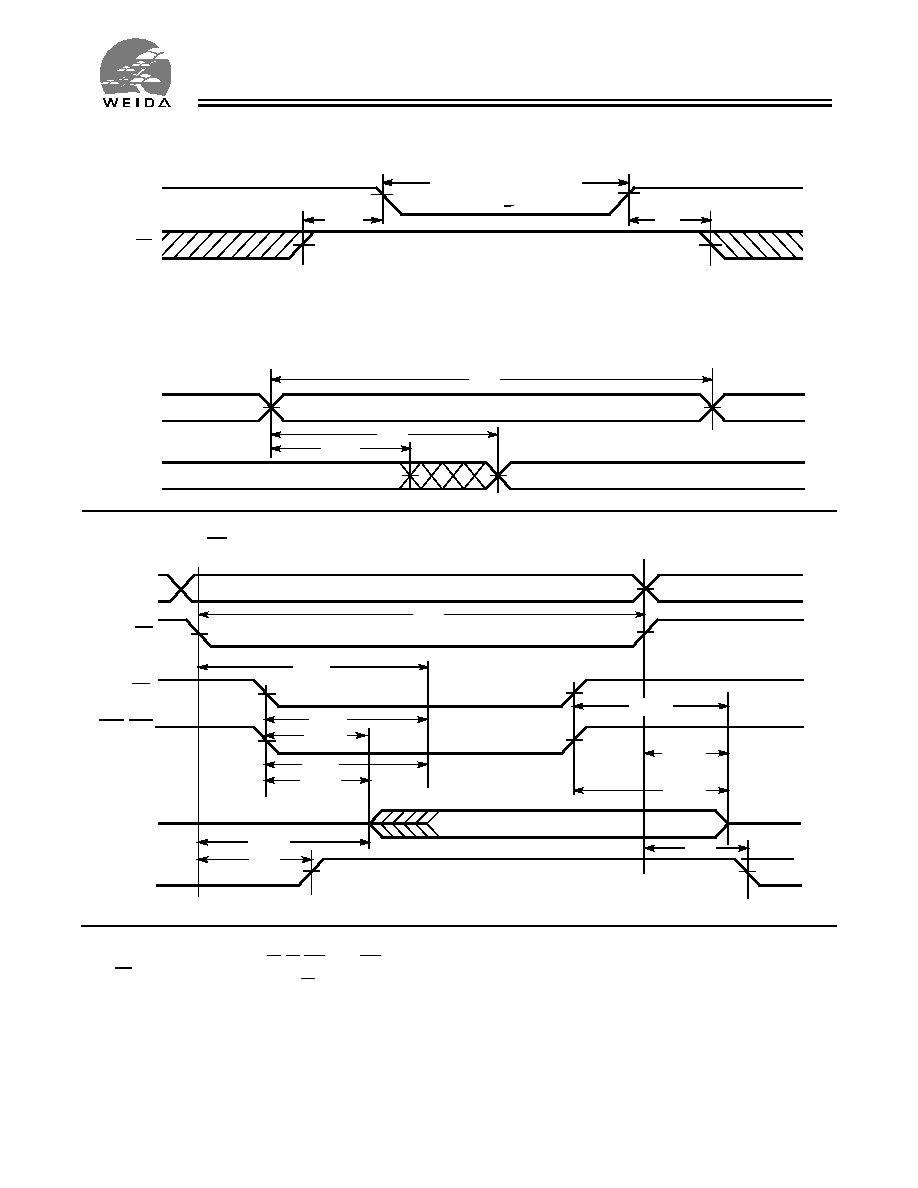
AC Test Loads and Waveforms
90%
10%
3.0V
GND
90%
10%
ALL INPUT PULSES
3.3V
OUTPUT
30 pF
INCLUDING
JIG AND
SCOPE
3.3V
OUTPUT
5 pF
INCLUDING
JIG AND
SCOPE
(a)
(b)
OUTPUT
R 317
R 317
R2
351
R2
351
167
Equivalent to: TH…VENIN
EQUIVALENT
1.73V
30 pF
Rise Time: 1 V/ns
Fall Time: 1 V/ns
WCFS1016V1C
Page 4 of 9
Switching Characteristics
[4]
Over the Operating Range
Parameter
Description
WCFS1016V1C 12ns
Unit
Min.
Max.
READ CYCLE
t
RC
Read Cycle Time
12
ns
t
AA
Address to Data Valid
12
ns
t
OHA
Data Hold from Address Change
3
ns
t
ACE
CE LOW to Data Valid
12
ns
t
DOE
OE LOW to Data Valid
6
ns
t
LZOE
OE LOW to Low Z
0
ns
t
HZOE
OE HIGH to High Z
[5, 6]
6
ns
t
LZCE
CE LOW to Low Z
[6]
3
ns
t
HZCE
CE HIGH to High Z
[5, 6]
6
ns
t
PU
CE LOW to Power-Up
0
ns
t
PD
CE HIGH to Power-Down
12
ns
t
DBE
Byte Enable to Data Valid
6
ns
t
LZBE
Byte Enable to Low Z
0
ns
t
HZBE
Byte Disable to High Z
6
ns
WRITE CYCLE
[7]
t
WC
Write Cycle Time
12
ns
t
SCE
CE LOW to Write End
9
ns
t
AW
Address Set-Up to Write End
8
ns
t
HA
Address Hold from Write End
0
ns
t
SA
Address Set-Up to Write Start
0
ns
t
PWE
WE Pulse Width
8
ns
t
SD
Data Set-Up to Write End
6
ns
t
HD
Data Hold from Write End
0
ns
t
LZWE
WE HIGH to Low Z
[6]
3
ns
t
HZWE
WE LOW to High Z
[5, 6]
6
ns
t
BW
Byte Enable to End of Write
8
ns
Data Retention Characteristics
Over the Operating Range
Parameter
Description
Conditions
[8]
Min.
Max.
Unit
V
DR
V
CC
for Data Retention
2.0
V
t
CDR
[9]
Chip Deselect to Data Retention Time V
CC
= V
DR
= 2.0V,
CE > V
CC
≠ 0.3V,
V
IN
> V
CC
≠ 0.3V or V
IN
< 0.3V
0
ns
t
R
[10]
Operation Recovery Time
t
RC
ns
Notes:
4.
Test conditions assume signal transition time of 3 ns or less, timing reference levels of 1.5V, input pulse levels of 0 to 3.0V, and output loading of the specified
I
OL
/I
OH
and 30-pF load capacitance.
5.
t
HZOE
, t
HZBE
, t
HZCE
, and t
HZWE
are specified with a load capacitance of 5 pF as in part (b) of AC Test Loads. Transition is measured
±
500 mV from steady-state voltage.
6.
At any given temperature and voltage condition, t
HZCE
is less than t
LZCE
, t
HZOE
is less than t
LZOE
, and t
HZWE
is less than t
LZWE
for any given device.
7.
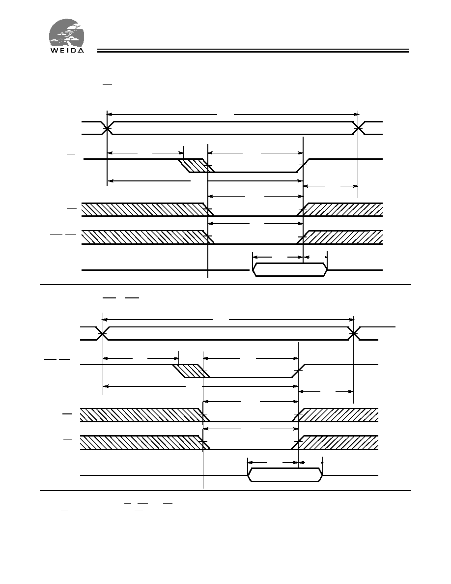
The internal write time of the memory is defined by the overlap of CE LOW, WE LOW and BHE / BLE LOW. CE, WE and BHE / BLE must be LOW to initiate a write,
and the transition of these signals can terminate the write. The input data set-up and hold timing should be referenced to the leading edge of the signal that terminates the write.
8.
No input may exceed V
CC
+ 0.5V.
9.
Tested initially and after any design or process changes that may affect these parameters.
10. t
r
< 3 ns for the -12 and -15 speeds. t
r
< 5 ns for the -20 and slower speeds.
WCFS1016V1C
Page 5 of 9
Data Retention Waveform
3.0V
3.0V
t
CDR
V
DR
>
2V
DATA RETENTION MODE
t
R
CE
V
CC
Switching Waveforms
Notes:
11. Device is continuously selected. OE, CE, BHE and/or BHE = V
IL
.
12. WE is HIGH for read cycle.
13. Address valid prior to or coincident with CE transition LOW.
Read Cycle No. 1
PREVIOUS DATA VALID
DATA VALID
t
RC
t
AA
t
OHA
ADDRESS
DATA OUT
[11, 12]
Read Cycle No. 2 (OE Controlled)
50%
50%
DATA VALID
t
RC
t
ACE
t
DOE
t
LZOE
t
LZCE
t
PU
HIGH IMPEDANCE
t
HZOE
t
HZBE
t
PD
HIGH
OE
CE
ICC
ISB
IMPEDANCE
ADDRESS
DATA OUT
V
CC
SUPPLY
t
DBE
t
LZBE
t
HZCE
BHE, BLE
[12, 13]
CURRENT
I
CC
I
SB
WCFS1016V1C
Page 6 of 9
Notes:
14. Data I/O is high impedance if OE or BHE and/or BLE= V
IH
.
15. If CE goes HIGH simultaneously with WE going HIGH, the output remains in a high-impedance state.
Switching Waveforms
(continued)
Write Cycle No. 1 (CE Controlled)
t
HD
t
SD
t
SCE
t
SA
t
HA
t
AW
t
PWE
t
WC
BW
DATA I/O
ADDRESS
CE
WE
BHE, BLE
[14, 15]
t
Write Cycle No. 2 (BLE or BHE Controlled)
t
HD
t
SD
t
BW
t
SA
t
HA
t
AW
t
PWE
t
WC
t
SCE
DATA I/O
ADDRESS
BHE, BLE
WE
CE
WCFS1016V1C
Page 7 of 9
Switching Waveforms
(continued)
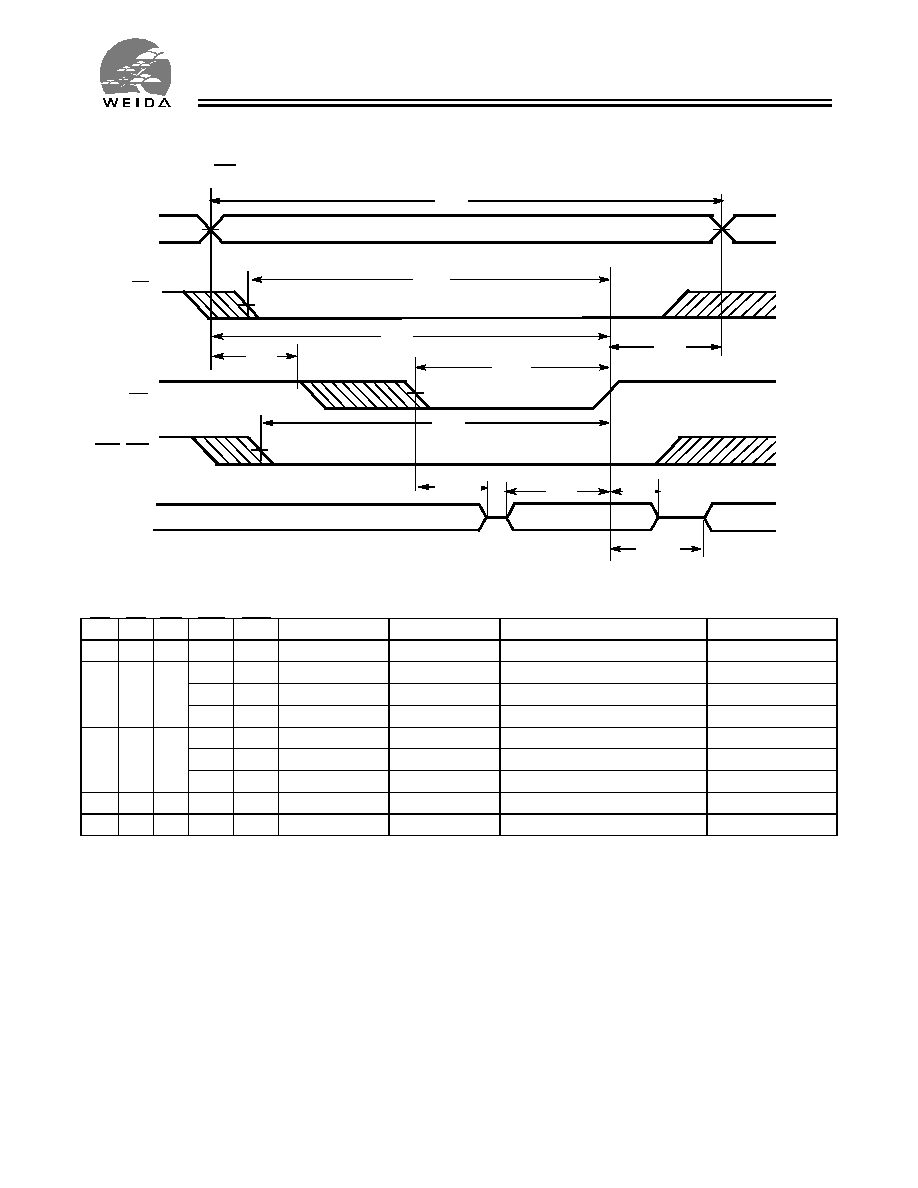
Write Cycle No. 3 (WE Controlled, LOW)
t
HD
t
SD
t
SCE
t
HA
t
AW
t
PWE
t
WC
t
BW
DATA I/O
ADDRESS
CE
WE
BHE, BLE
t
SA
t
LZWE
t
HZWE
Truth Table
CE
OE
WE
BLE
BHE
I/O
1
≠I/O
8
I/O
9
≠I/O
16
Mode
Power
H
X
X
X
X
High Z
High Z
Power-Down
Standby (I
SB
)
L
L
H
L
L
Data Out
Data Out
Read - All bits
Active (I
CC
)
L
H
Data Out
High Z
Read - Lower bits only
Active (I
CC
)
H
L
High Z
Data Out
Read - Upper bits only
Active (I
CC
)
L
X
L
L
L
Data In
Data In
Write - All bits
Active (I
CC
)
L
H
Data In
High Z
Write - Lower bits only
Active (I
CC
)
H
L
High Z
Data In
Write - Upper bits only
Active (I
CC
)
L
H
H
X
X
High Z
High Z
Selected, Outputs Disabled
Active (I
CC
)
L
X
X
H
H
High Z
High Z
Selected, Outputs Disabled
Active (I
CC
)
WCFS1016V1C
Page 8 of 9
Ordering Information
Speed (ns)
Ordering Code
Package
Name
Package Type
Operating
Range
12
WCFS1016V1C-JC12
J
44-Lead (400-Mil) Molded SOJ
Commercial
Package Diagrams
44-Lead (400-Mil) Molded SOJ J

WCFS1016V1C
Page 9 of 9
Document Title: WCFS1016V1C 64K x 16 Static RAM
REV.
Issue Date
Orig. of Change
Description of Change
**
4/19/02
XFL
NEW DATASHEET