512K x 8 Static RAM
WCFS4008V1C
S4008V1C
Features
∑ High speed
-- t
AA
= 12 ns
∑ 2.0V Data Retention
∑ Automatic power-down when deselected
∑ TTL-compatible inputs and outputs
∑ Easy memory expansion with CE and OE features
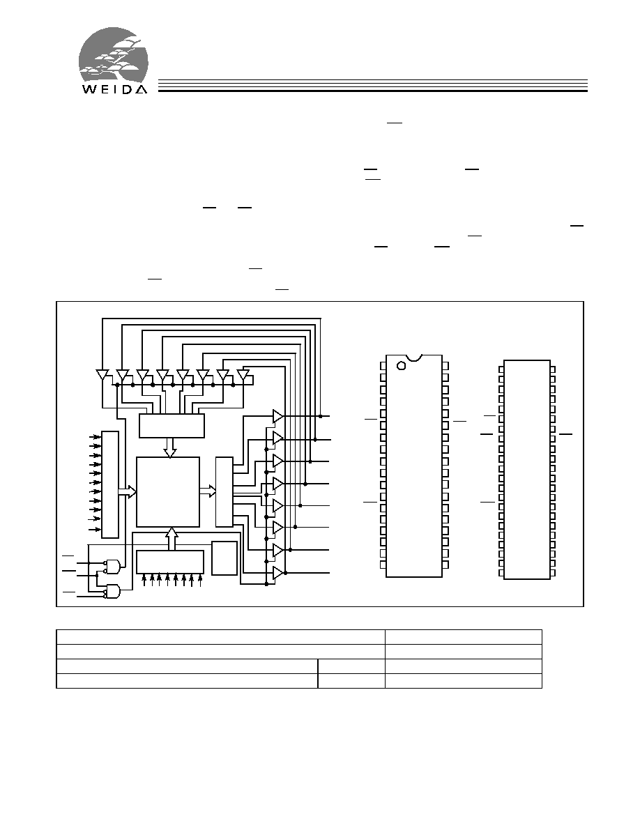
Functional Description
The WCFS4008V1C is a high-performance CMOS Static RAM
organized as 524K words by 8 bits. Easy memory expansion
is provided by an active LOW Chip Enable (CE), an active
LOW Output Enable (OE), and three-state drivers. Writing to
the device is accomplished by taking Chip Enable (CE) and
Write Enable (WE) inputs LOW. Data on the eight I/O pins (I/O
0
through I/O
7
) is then written into the location specified on the
address pins (A
0
through A
18
).
Reading from the device is accomplished by taking Chip
Enable (CE) and Output Enable (OE) LOW while forcing Write
Enable (WE) HIGH. Under these conditions, the contents of
the memory location specified by the address pins will appear
on the I/O pins.
The eight input/output pins (I/O
0
through I/O
7
) are placed in a
high-impedance state when the device is deselected (CE
HIGH), the outputs are disabled (OE HIGH), or during a write
operation (CE LOW, and WE LOW).
The WCFS4008V1C is available in standard 400-mil-wide
36-pin SOJ package and 44-pin TSOP II package with center
power and ground pinout.
14
15
Logic Block Diagram
Pin Configuration
A
1
A
2
A
3
A
4
A
5
A
6
A
7
A
8
COLUMN
DECODER
ROW DE
CODER
SE
N
S
E A
M
PS
INPUT BUFFER
POWER
DOWN
WE
OE
I/O
0
I/O
1
I/O
2
I/O
3
512K x 8
ARRAY
I/O
7
I/O
6
I/O
5
I/O
4
A
0
A
11
A
13
A
12
A
CE
A
A
16
A
17
1
2
3
4
5
6
7
8
9
10
11
14
23
24
28
27
26
25
29
32
31
30
Top View
SOJ
12
13
33
36
35
34
16
15
21
22
GND
A
1
A
2
A
3
A
4
A
5
A
6
A
7
A
8
WE
V
CC
A
18
A
15
A
12
A
14
I/O
5
I/O
4
A
9
A
0
I/O
0
I/O
1
I/O
2
OE
A
17
A
16
A
13
CE
A
9
A
18
18
17
19
20
GND
I/O
7
I/O3
I/O
6
V
CC
A
10
A
11
NC
NC
A
10
A
6
1
2
3
4
5
6
7
8
9
10
11
14
31
32
36
35
34
33
37
40
39
38
Top View
TSOP II
12
13
41
44
43
42
16
15
29
30
V
CC
A
7
A
8
A
9
NC
NC
NC
NC
A
18
V
SS
NC
A
15
A
0
A
3
I/O
0
A
4
CE
A
17
A
12
A
1
A
2
18
17
20
19
I/O
1
27
28
25
26
22
21
23
24
NC
V
SS
WE
I/O
2
I/O
3
A
5
NC
A
16
V
CC
OE
I/O
7
I/O
6
I/O
5
I/O
4
A
14
A
13
A
11
A
10
NC
NC
NC
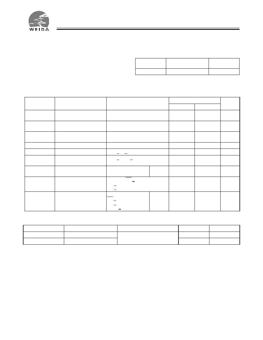
Selection Guide
WCFS4008V1C 12ns
Maximum Access Time (ns)
12
Maximum Operating Current (mA)
Comm'l
85
Maximum CMOS Standby Current (mA)
Comm'l
10
WCFS4008V1C
2
Maximum Ratings
(Above which the useful life may be impaired. For user guide-
lines, not tested.)
Storage Temperature ................................≠65◊C to +150◊C
Ambient Temperature with
Power Applied............................................≠55◊C to +125◊C
Supply Voltage on V
CC
to Relative GND
[1]
.... ≠0.5V to +4.6V
DC Voltage Applied to Outputs
in High Z State
[1]
....................................≠0.5V to V
CC
+ 0.5V
DC Input Voltage
[1]
................................ ≠0.5V to V
CC
+ 0.5V
Current into Outputs (LOW) ........................................ 20 mA
Operating Range
Range
Ambient
Temperature
V
CC
Commercial
0
∞
C to +70
∞
C
3.3V
±
0.3V
Electrical Characteristics
Over the Operating Range
Parameter
Description
Test Conditions
WCFS4008V1C 12ns
Min.
Max.
Unit
V
OH
Output HIGH Voltage
V
CC
= Min.,
I
OH
= ≠4.0 mA
2.4
V
V
OL
Output LOW Voltage
V
CC
= Min.,
I
OL
= 8.0 mA
0.4
V
V
IH
Input HIGH Voltage
2.0
V
CC
+ 0.3
V
V
IL
Input LOW Voltage
[1]
≠0.3
0.8
V
I
IX
Input Load Current
GND < V
I
< V
CC
≠1
+1
µ
A
I
OZ
Output Leakage
Current
GND < V
OUT
< V
CC
,
Output Disabled
≠1
+1
µ
A
I
CC
V
CC
Operating
Supply Current
V
CC
= Max.,
f = f
MAX
= 1/t
RC
Comm'l
85
mA
I
SB1
Automatic CE
Power-Down Current
--TTL Inputs
Max. V
CC
, CE > V
IH
V
IN
> V
IH
or
V
IN
< V
IL
, f = f
MAX
40
mA
I
SB2
Automatic CE
Power-Down Current
--CMOS Inputs
Max. V
CC
,
CE > V
CC
≠ 0.3V,
V
IN
> V
CC
≠ 0.3V,
or V
IN
< 0.3V, f = 0
Comm'll
10
mA
Capacitance
[2]
Parameter
Description
Test Conditions
Max.
Unit
C
IN
Input Capacitance
T
A
= 25
∞
C, f = 1 MHz,
V
CC
= 3.3V
8
pF
C
OUT
I/O Capacitance
8
pF
Note:
1.
V
IL
(min.) = ≠2.0V for pulse durations of less than 20 ns
2.
Tested initially and after any design or process changes that may affect these parameters.
WCFS4008V1C
3
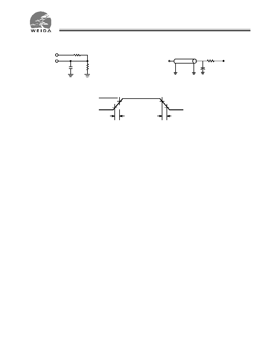
AC Test Loads and Waveforms
* CAPACITIVE LOAD CONSISTS
OF ALL COMPONENTS OF THE
TEST ENVIRONMENT
3.3V
OUTPUT
5 pF
INCLUDING
JIG AND
SCOPE
(a)
R1 317
R2
351
OUTPUT
50
Z
0
=50
V
TH
= 1.5V
30pF*
(c)
(b)
90%
10%
3.3V
GND
90%
10%
ALL INPUT PULSES
Rise time > 1 V/ns
Fall time:
> 1 V/ns
WCFS4008V1C
4
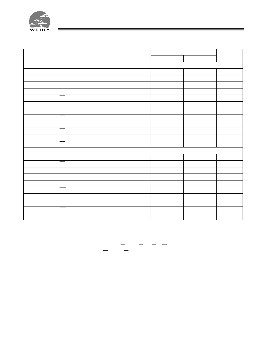
AC Switching Characteristics
[3]
Over the Operating Range
WCFS4008V1C 12ns
Parameter
Description
Min.
Max.
Unit
READ CYCLE
t
power
[4]
V
CC
(typical) to the first access
1
ns
t
RC
Read Cycle Time
12
ns
t
AA
Address to Data Valid
12
ns
t
OHA
Data Hold from Address Change
3
ns
t
ACE
CE LOW to Data Valid
12
ns
t
DOE
OE LOW to Data Valid
6
ns
t
LZOE
OE LOW to Low Z
0
ns
t
HZOE
OE HIGH to High Z
[5, 6]
6
ns
t
LZCE
CE LOW to Low Z
[6]
3
ns
t
HZCE
CE HIGH to High Z
[5, 6]
6
ns
t
PU
CE LOW to Power-Up
0
ns
t
PD
CE HIGH to Power-Down
12
ns
WRITE CYCLE
[7, 8]
t
WC
Write Cycle Time
12
ns
t
SCE
CE LOW to Write End
8
ns
t
AW
Address Set-Up to Write End
8
ns
t
HA
Address Hold from Write End
0
ns
t
SA
Address Set-Up to Write Start
0
ns
t
PWE
WE Pulse Width
8
ns
t
SD
Data Set-Up to Write End
6
ns
t
HD
Data Hold from Write End
0
ns
t
LZWE
WE HIGH to Low Z
[6]
3
ns
t
HZWE
WE LOW to High Z
[5, 6]
6
ns
Notes:
3.
Test conditions assume signal transition time of 3 ns or less, timing reference levels of 1.5V, input pulse levels of 0 to 3.0V.
4.
t
POWER
gives the minimum amount of time that the power supply should be at stable, typical Vcc values until the first memory access can be performed.
5.
t
HZOE
, t
HZCE
, and t
HZWE
are specified with a load capacitance of 5 pF as in part (b) of AC Test Loads. Transition is measured
±
500 mV from steady-state voltage.
6.
At any given temperature and voltage condition, t
HZCE
is less than t
LZCE
, t
HZOE
is less than t
LZOE
, and t
HZWE
is less than t
LZWE
for any given device.
7.
The internal write time of the memory is defined by the overlap of CE LOW, and WE LOW. CE and WE must be LOW to initiate a write, and the transition of either of
these signals can terminate the write. The input data set-up and hold timing should be referenced to the leading edge of the signal that terminates the write.
8.
The minimum write cycle time for Write Cycle No. 3 (WE controlled, OE LOW) is the sum of t
HZWE
and t
SD
.
WCFS4008V1C
5
Switching Waveforms
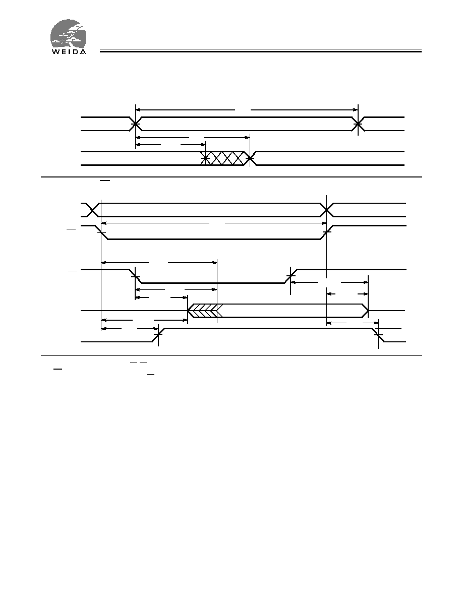
Read Cycle No. 1
[9, 10]
Read Cycle No. 2 (OE Controlled)
[10, 11]
Notes:
9.
Device is continuously selected. OE, CE = V
IL
.
10. WE is HIGH for read cycle.
11. Address valid prior to or coincident with CE transition LOW.
PREVIOUS DATA VALID
DATA VALID
t
RC
t
AA
t
OHA
ADDRESS
DATA OUT
50%
50%
DATA VALID
t
RC
t
ACE
t
DOE
t
LZOE
t
LZCE
t
PU
HIGH IMPEDANCE
t
HZOE
t
HZCE
t
PD
HIGH
OE
CE
I
CC
I
SB
IMPEDANCE
ADDRESS
DATA OUT
V
CC
SUPPLY
CURRENT
WCFS4008V1C
6
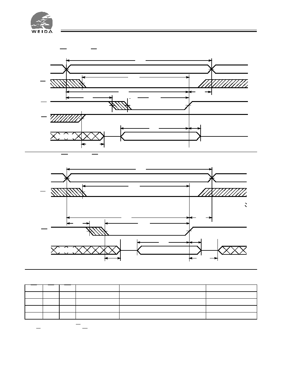
Write Cycle No. 1(WE Controlled, OE HIGH During Write)
[12, 13]
Write Cycle No. 2 (WE Controlled, OE LOW)
[13]
Switching Waveforms
(continued)
t
HD
t
SD
t
PWE
t
SA
t
HA
t
AW
t
SCE
t
WC
t
HZOE
DATA
IN
VALID
CE
ADDRESS
WE
DATA I/O
OE
NOTE
14
DATA VALID
t
HD
t
SD
t
LZWE
t
PWE
t
SA
t
HA
t
AW
t
SCE
t
WC
t
HZWE
CE
ADDRESS
WE
DATA I/O
NOTE
14
Truth Table
CE
OE
WE
I/O
0
≠ I/O
7
Mode
Power
H
X
X
High Z
Power-Down
Standby (I
SB
)
L
L
H
Data Out
Read
Active (I
CC
)
L
X
L
Data In
Write
Active (I
CC
)
L
H
H
High Z
Selected, Outputs Disabled
Active (I
CC
)
Notes:
12. Data I/O is high-impedance if OE = V
IH
.
13. If CE goes HIGH simultaneously with WE going HIGH, the output remains in a high-impedance state.
14. During this period the I/Os are in the output state and input signals should not be applied.
WCFS4008V1C
7
Ordering Information
Speed
(ns)
Ordering Code
Package
Name
Package Type
Operating
Range
12
WCFS4008V1C-JC12
J
36-Lead (400-Mil) Molded SOJ
Commercial
WCFS4008V1C-TC12
T
44-pin TSOP II
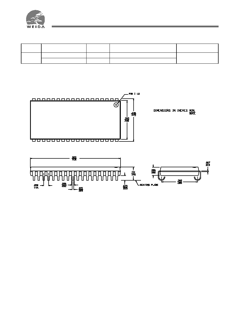
Package Diagrams
36-Lead (400-Mil) Molded SOJ J
WCFS4008V1C
8
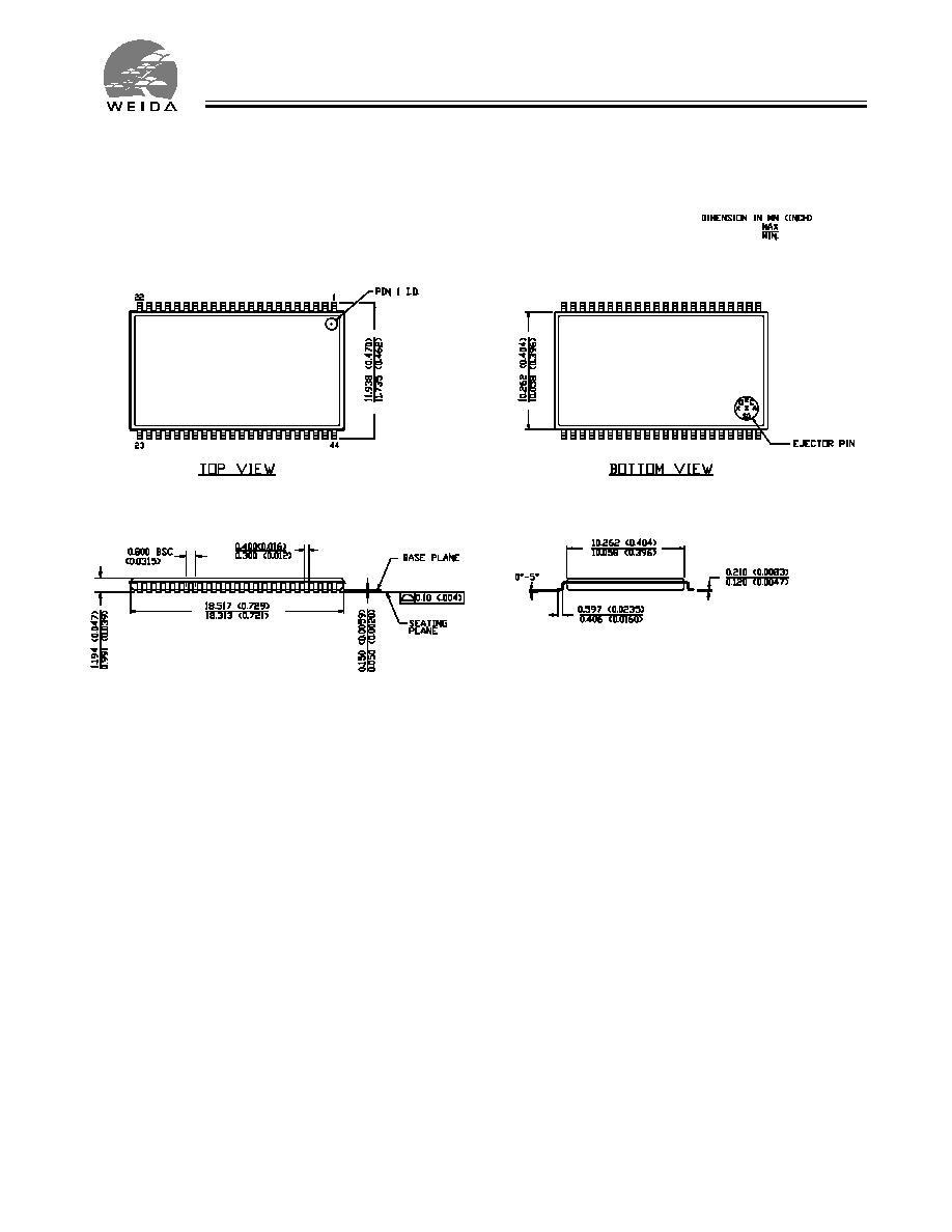
Package Diagrams
(continued)
44-Pin TSOP II T
512K x 8 Static RAM
WCFS4008V1C
Revision History
Document Title: WCFS4008V1C 32K x 8 3.3V Static RAM
REV.
ISSUE DATE
ORIG. OF CHANGE
DESCRIPTION OF CHANGE
**
4/12/2002
XFL
New Datasheet