
256K x 16 Static RAM
WCFS4016C1C
Revised April 19, 2002
1041B
Features
∑ High speed
-- t
AA
= 15 ns
∑ 2.0V Data Retention (400
µ
W at 2.0V retention)
∑ Automatic power-down when deselected
∑ TTL-compatible inputs and outputs
∑ Easy memory expansion with CE and OE features
Functional Description
The WCFS4016C1C is a high-performance CMOS static RAM
organized as 262,144 words by 16 bits.
Writing to the device is accomplished by taking Chip Enable
(CE) and Write Enable (WE) inputs LOW. If Byte Low Enable
(BLE) is LOW, then data from I/O pins (I/O
0
through I/O
7
), is
written into the location specified on the address pins (A
0
through A
17
). If Byte High Enable (BHE) is LOW, then data
from I/O pins (I/O
8
through I/O
15
) is written into the location
specified on the address pins (A
0
through A
17
).
Reading from the device is accomplished by taking Chip En-
able (CE) and Output Enable (OE) LOW while forcing the Write
Enable (WE) HIGH. If Byte Low Enable (BLE) is LOW, then
data from the memory location specified by the address pins
will appear on I/O
0
to I/O
7
. If Byte High Enable (BHE) is LOW,
then data from memory will appear on I/O
8
to I/O
15
. See the
truth table at the back of this data sheet for a complete descrip-
tion of read and write modes.
The input/output pins (I/O
0
through I/O
15
) are placed in a
high-impedance state when the device is deselected (CE
HIGH), the outputs are disabled (OE HIGH), the BHE and BLE
are disabled (BHE, BLE HIGH), or during a write operation (CE
LOW, and WE LOW).
The WCFS4016C1C is available in a standard 44-pin
400-mil-wide SOJ package.
14
15
Logic Block Diagram
Pin Configuration
A
1
A
2
A
3
A
4
A
5
A
6
A
7
A
8
COLUMN
DECODER
ROW DECODER
S
E
NS
E AM
PS
INPUT BUFFER
256K x 16
ARRAY
A
0
A
11
A
13
A
12
A
A
A
16
A
17
A
9
A
10
1024 x 4096
I/O
0
≠ I/O
7
OE
I/O
8
≠ I/O
15
CE
WE
BLE
BHE
WE
1
2
3
4
5
6
7
8
9
10
11
14
31
32
36
35
34
33
37
40
39
38
Top View
SOJ
12
13
41
44
43
42
16
15
29
30
V
CC
A
5
A
6
A
7
A
8
A
0
A
1
OE
V
SS
A
17
I/O
15
A
2
CE
I/O
2
I/O
0
I/O
1
BHE
A
3
A
4
18
17
20
19
I/O
3
27
28
25
26
22
21
23
24
V
SS
I/O
6
I/O
4
I/O
5
I/O
7
A
16
A
15
BLE
V
CC
I/O
14
I/O
13
I/O
12
I/O
11
I/O
10
I/O
9
I/O
8
A
14
A
13
A
12
A
11
A
9
A
10
NC
Selection Guide
WCFS4016C1C 15ns
Maximum Access Time (ns)
15
Maximum Operating Current (mA)
190
Maximum CMOS Standby Current (mA)
3

WCFS4016C1C
Page 2 of 10
Maximum Ratings
(Above which the useful life may be impaired. For user guide-
lines, not tested.)
Storage Temperature ≠65
∞
C to +150
∞
C
Ambient Temperature with
Power Applied≠55
∞
C to +125
∞
C
Supply Voltage on V
CC
to Relative GND
[1]
≠0.5V to +7.0V
DC Voltage Applied to Outputs
in High Z State
[1]
≠0.5V to V
CC
+ 0.5V
DC Input Voltage
[1]
≠0.5V to V
CC
+ 0.5V
Current into Outputs (LOW)20 mA
Operating Range
Range
Ambient
Temperature
[2]
V
CC
Commercial
0
∞
C to +70
∞
C
5V
±
0.5
Electrical Characteristics
Over the Operating Range
Parameter
Description
Test Conditions
WCFS4016C1C 15ns
Min.
Max.
Unit
V
OH
Output HIGH Voltage
V
CC
= Min., I
OH
= ≠4.0 mA
2.4
V
V
OL
Output LOW Voltage
V
CC
= Min., I
OL
= 8.0 mA
0.4
V
V
IH
Input HIGH Voltage
2.2
V
CC
+ 0.5
V
V
IL
Input LOW Voltage
[1]
≠0.5
0.8
V
I
IX
Input Load Current
GND < V
I
< V
CC
≠1
+1
µ
A
I
OZ
Output Leakage
Current
GND < V
OUT
< V
CC
,
Output Disabled
≠1
+1
µ
A
I
CC
V
CC
Operating
Supply Current
V
CC
= Max.,
f = f
MAX
= 1/t
RC
190
mA
I
SB1
Automatic CE
Power-Down Current
--TTL Inputs
Max. V
CC
, CE > V
IH
V
IN
> V
IH
or
V
IN
< V
IL
, f = f
MAX
40
mA
I
SB2
Automatic CE
Power-Down Current
--CMOS Inputs
Max. V
CC
,
CE > V
CC
≠ 0.3V,
V
IN
> V
CC
≠ 0.3V,
or V
IN
< 0.3V, f = 0
3
mA

WCFS4016C1C
Page 3 of 10
Capacitance
[3]
Parameter
Description
Test Conditions
Max.
Unit
C
IN
Input Capacitance
T
A
= 25
∞
C, f = 1 MHz,
V
CC
= 5.0V
8
pF
C
OUT
I/O Capacitance
8
pF
AC Test Loads and Waveforms
Note:
1.
V
IL
(min.) = ≠2.0V for pulse durations of less than 20 ns.
2.
T
A
is the case temperature.
3.
Tested initially and after any design or process changes that may affect these parameters.
90%
10%
3.0V
GND
90%
10%
ALL INPUT PULSES
5V
OUTPUT
30 pF
INCLUDING
JIG AND
SCOPE
5V
OUTPUT
5 pF
INCLUDING
JIG AND
SCOPE
(a)
(b)
3 ns
3 ns
OUTPUT
R1 481
R1 481
R2
255
R2
255
167
Equivalent to:
VENIN EQUIVALENT
1.73V
TH…

WCFS4016C1C
Page 4 of 10
Switching Characteristics
[4]
Over the Operating Range
WCFS4016C1C 15ns
Parameter
Description
Min.
Max.
Unit
READ CYCLE
t
power
V
CC
(typical) to the First Access
[5]
1
ms
t
RC
Read Cycle Time
15
ns
t
AA
Address to Data Valid
15
ns
t
OHA
Data Hold from Address Change
3
ns
t
ACE
CE LOW to Data Valid
15
ns
t
DOE
OE LOW to Data Valid
7
ns
t
LZOE
OE LOW to Low Z
0
ns
t
HZOE
OE HIGH to High Z
[6, 7]
7
ns
t
LZCE
CE LOW to Low Z
[7]
3
ns
t
HZCE
CE HIGH to High Z
[6, 7]
7
ns
t
PU
CE LOW to Power-Up
0
ns
t
PD
CE HIGH to Power-Down
15
ns
t
DBE
Byte Enable to Data Valid
7
ns
t
LZBE
Byte Enable to Low Z
0
ns
t
HZBE
Byte Disable to High Z
7
ns
WRITE CYCLE
[8, 9]
t
WC
Write Cycle Time
15
ns
t
SCE
CE LOW to Write End
12
ns
t
AW
Address Set-Up to Write End
12
ns
t
HA
Address Hold from Write End
0
ns
t
SA
Address Set-Up to Write Start
0
ns
t
PWE
WE Pulse Width
12
ns
t
SD
Data Set-Up to Write End
8
ns
t
HD
Data Hold from Write End
0
ns
t
LZWE
WE HIGH to Low Z
[7]
3
ns
t
HZWE
WE LOW to High Z
[6, 7]
7
ns
t
BW
Byte Enable to End of Write
12
ns
Notes:
4.
Test conditions assume signal transition time of 3 ns or less, timing reference levels of 1.5V, input pulse levels of 0 to 3.0V, and output loading of the specified
I
OL
/I
OH
and 30-pF load capacitance.
5.
This part has a voltage regulator which steps down the voltage from 5V to 3.3V internally. t
power
time has to be provided initially before a read/write operation
is started.
6.
t
HZOE
, t
HZCE
, and t
HZWE
are specified with a load capacitance of 5 pF as in part (b) of AC Test Loads. Transition is measured
±
500 mV from steady-state voltage.
7.
At any given temperature and voltage condition, t
HZCE
is less than t
LZCE
, t
HZOE
is less than t
LZOE
, and t
HZWE
is less than t
LZWE
for any given device.
8.
The internal write time of the memory is defined by the overlap of CE LOW, and WE LOW. CE and WE must be LOW to initiate a write, and the transition of either of
these signals can terminate the write. The input data set-up and hold timing should be referenced to the leading edge of the signal that terminates the write.
9.
The minimum write cycle time for Write Cycle no. 3 (WE controlled, OE LOW) is the sum of t
HZWE
and t
SD
.
WCFS4016C1C
Page 5 of 10
Data Retention Characteristics
Over the Operating Range
Parameter
Description
Conditions
[11]
Min.
Max.
Unit
V
DR
V
CC
for Data Retention
2.0
V
t
CDR
[3]
Chip Deselect to Data Retention Time
V
CC
= V
DR
= 3.0V,
CE > V
CC
≠ 0.3V,
V
IN
> V
CC
≠ 0.3V or V
IN
< 0.3V
0
ns
t
R
[10]
Operation Recovery Time
t
RC
ns
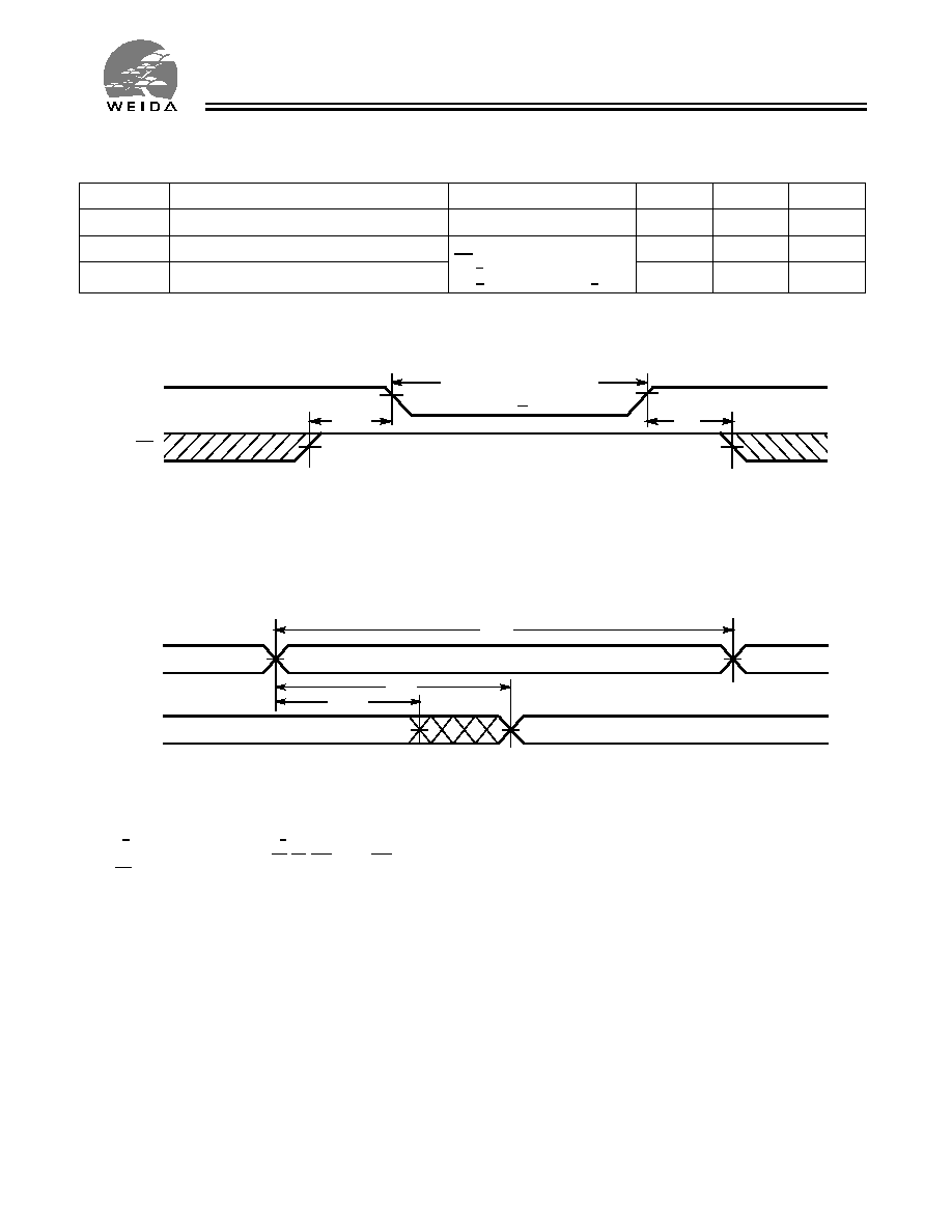
Data Retention Waveform
Switching Waveforms
Notes:
10. t
r
< 3 ns for the -12 and -15 speeds. t
r
< 5 ns for the -20 and slower speeds
11. No input may exceed V
CC
+ 0.5V
12. Device is continuously selected. OE, CE, BHE, and/or BHE = V
IL
..
13. WE is HIGH for read cycle.
3.0V
3.0V
t
CDR
V
DR
> 2V
DATA RETENTION MODE
t
R
CE
V
CC
Read Cycle No. 1
PREVIOUS DATA VALID
DATA VALID
t
RC
t
AA
t
OHA
ADDRESS
DATA OUT
[12, 13]