128K x 8 Static RAM
WCMA1008U1X
A1008U1X
Features
∑ High Speed
-- 55ns and 70ns availability
∑ Voltage range
-- 2.7V≠3.6V
∑ Ultra low active power
-- Typical active current: 20 mA @ f = f
max
(70ns speed)
∑ Low standby power
∑ Easy memory expansion with CE and OE features
∑ Automatic power-down when deselected
∑ CMOS for optimum speed/power
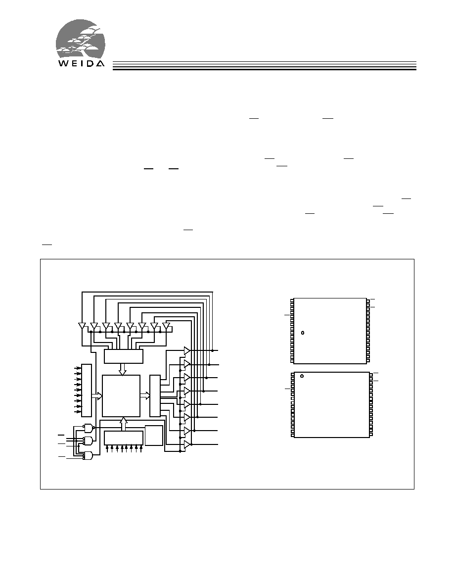
Functional Description
The WCMA1008U1X is a high-performance CMOS static
RAM organized as 128K words by 8 bits. Easy memory expan-
sion is provided by an active LOW Chip Enable (CE
1
), an ac-
tive HIGH Chip Enable (CE
2
), an active LOW Output Enable
(OE) and three-state drivers. These devices have an automat-
ic power-down feature, reducing the power consumption by
over 99% when deselected.
Writing to the device is accomplished by taking Chip Enable
one (CE
1
) and Write Enable (WE) inputs LOW and the Chip
Enable two (CE
2
) input HIGH. Data on the eight I/O pins (I/O
0
through I/O
7
) is then written into the location specified on the
address pins (A
0
through A
16
).
Reading from the device is accomplished by taking Chip En-
able one (CE
1
) and Output Enable (OE) LOW while forcing
Write Enable (WE) and Chip Enable two (CE
2
) HIGH. Under
these conditions, the contents of the memory location speci-
fied by the address pins will appear on the I/O pins.
The eight input/output pins (I/O
0
through I/O
7
) are placed in a
high-impedance state when the device is deselected (CE
1
HIGH or CE
2
LOW), the outputs are disabled (OE HIGH), or
during a write operation (CE
1
LOW, CE
2
HIGH, and WE LOW).
The WCMA1008U1X is available in a 32 Lead TSOP and
STSOP packages.
Logic Block Diagram
A
6
A
7
A
16
A
14
A
12
WE
V
CC
A
4
A
13
A
8
A
9
OE
STSOP
Top View
(not to scale)
30
28
29
31
24
19
23
22
21
20
18
13
17
16
15
14
11
12
I/O
2
I/O
1
GND
I/O
7
I/O
4
I/O
5
I/O
6
I/O
0
CE
1
A
11
A
5
9
10
32
1
2
3
4
5
6
7
8
CE
2
A
15
NC
A
10
I/O
3
A
1
A
0
A
3
A
2
26
25
26
27
A
6
A
7
A
16
A
14
A
12
WE
V
CC
A
4
A
13
A
8
A
9
OE
TSOP I
Top View
(not to scale)
1
6
2
3
4
5
7
32
27
31
30
29
28
26
21
25
24
23
22
19
20
I/O
2
I/O
1
GND
I/O
7
I/O
4
I/O
5
I/O
6
I/O
0
CE
1
A
11
A
5
17
18
8
9
10
11
12
13
14
15
16
CE
2
A
15
NC
A
10
I/O
3
A
1
A
0
A
3
A
2
Pin Configurations
14
15
A
1
A
2
A
3
A
4
A
5
A
6
A
7
A
8
COLUMN
DECODER
ROW DEC
O
D
E
R
SE
N
S
E AM
PS
INPUT BUFFER
POWER
DOWN
WE
OE
I/O
0
CE
2
I/O
1
I/O
2
I/O
3
512x 256x 8
ARRAY
I/O
7
I/O
6
I/O
5
I/O
4
A
0
A
11
A
13
A
12
A
A
10
CE
1
A A
16
A
9

WCMA1008U1X
2
Maximum Ratings
(Above which the useful life may be impaired. For user guide-
lines, not tested.)
Storage Temperature .................................≠65∞C to +150∞C
Ambient Temperature with
Power Applied...............................................55∞C to +125∞C
Supply Voltage to Ground Potential..... ..........≠0.5V to +4.6V
DC Voltage Applied to Outputs
in High Z State
[1]
........................................0.5V to V
CC
+ 0.5V
DC Input Voltage
[1]
..................................≠0.5V to V
CC
+ 0.5V
Output Current into Outputs (LOW)............................20 mA
Static Discharge Voltage ..........................................>2001V
(per MIL-STD-883, Method 3015)
Latch-Up Current ......................................................>200 mA
Notes:
1.
V
IL(min.)
= ≠2.0V for pulse durations less than 20 ns.
2.
Typical values are included for reference only and are not guaranteed or tested. Typical values are measured at V
CC
= V
CC(typ.)
, T
A
= 25∞C.
Operating Range
Product
Range
Ambient Temperature
V
CC
WCMA1008U1X
Industrial
≠40∞C to +85∞C
2.7V to 3.6V
Product Portfolio
Product
V
CC
Range
Speed
Power Dissipation (Industrial)
Operating, I
CC
Standby (I
SB2
)
f = f
max
Typ.
[2]
Max.
Min.
Typ.
[2]
Max.
Typ.
[2]
Max.
WCMA1008U1X
2.7V
3.0V
3.6V
70 ns
20 mA
40 mA
0.4
µ
A
30
µ
A
55 ns
WCMA1008U1X
3
Electrical Characteristics Over the Operating Range
WCMA1008U1X-70/55
Parameter
Description
Test Conditions
Min.
Typ.
[2]
Max.
Unit
V
OH
Output HIGH Voltage
I
OH
= ≠1.0 mA
V
CC
= 2.7V
2.4
V
V
OL
Output LOW Voltage
I
OL
= 2.1 mA
V
CC
= 2.7V
0.4
V
V
IH
Input HIGH Voltage
2
V
CC
+
0.5V
V
V
IL
Input LOW Voltage
≠0.5
0.8
V
I
IX
Input Leakage Cur-
rent
GND < V
I
< V
CC
≠1
+1
µ
A
I
OZ
Output Leakage Cur-
rent
GND < V
O
< V
CC
, Output Disabled
≠1
+1
µ
A
I
CC
V
CC
Operating Supply
Current
f = f
MAX
= 1/t
RC
V
CC
= 3.6V
I
OUT
= 0 mA
CMOS Levels
70ns
20
40
mA
55ns
23
50
I
SB1
Automatic CE
Power-Down Cur-
rent-- TTL Inputs
Max. V
CC
, CE
1
V
IH
,
CE
2
<V
IH
V
IN
> V
IH
or
V
IN
< V
IL
, f = f
MAX
70ns
15
300
µ
A
55ns
17
350
I
SB2
Automatic CE
Power-Down Cur-
rent-- CMOS Inputs
Max. V
CC
, CE
1
V
CC
≠ 0.3V,CE
2
<0.3
V
IN
> V
CC
≠ 0.3V or V
IN
< 0.3V, f = 0
0.4
30
Capacitance
[3]
Parameter
Description
Test Conditions
Max.
Unit
C
IN
Input Capacitance
T
A
= 25∞C, f = 1 MHz,V
CC
= Vcc
(typ)
6
pF
C
OUT
Output Capacitance
8
pF
Thermal Resistance
Description
Test Conditions
Symbol
BGA
Unit
Thermal Resistance
[3]
(Junction to Ambient)
Still Air, soldered on a 4.25 x 1.125 inch, 4-layer print-
ed circuit board
JA
55
∞
C/W
Thermal Resistance
[3]
(Junction to Case)
JC
16
∞
C/W
Note:
3.
Tested initially and after any design or process changes that may affect these parameters.
WCMA1008U1X
4
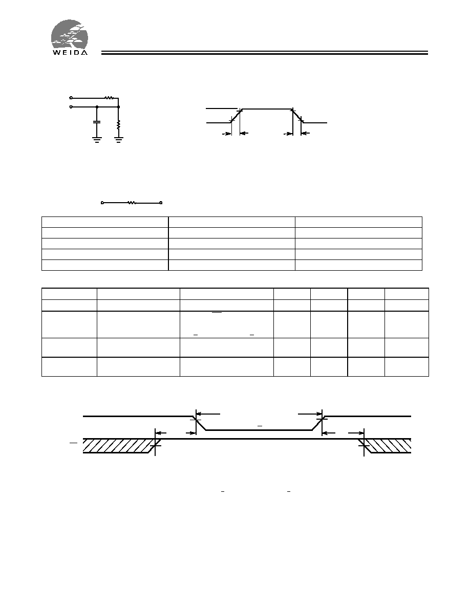
AC Test Loads and Waveforms
Parameters
3.3V
Unit
R1
1213
Ohms
R2
1378
Ohms
R
TH
645
Ohms
V
TH
1.75
Volts
Data Retention Characteristics
(Over the Operating Range)
Parameter
Description
Conditions
Min.
Typ.
[2]
Max.
Unit
V
DR
V
CC
for Data Retention
1.6
V
I
CCDR
Data Retention Current
V
CC
= 2V, CE
1
V
CC
≠ 0.3V,
CE
2
< 0.3V
V
IN
> V
CC
≠ 0.3V or V
IN
< 0.3V
0.4
20
µ
A
t
CDR
[3]
Chip Deselect to Data
Retention Time
0
ns
t
R
[4]
Operation Recovery
Time
t
RC
ns
Data Retention Waveform
Note:
4.
Full Device AC operation requires linear V
CC
ramp from V
DR
to V
CC(min.)
> 100
µ
s or stable at V
CC(min.)
>
100
µ
s.
V
CC
Typ
V
CC
OUTPUT
R2
30 pF
INCLUDING
JIG AND
SCOPE
GND
90%
10%
90%
10%
OUTPUT
V
TH
Equivalent to:
TH… VENIN EQUIVALENT
ALL INPUT PULSES
R
TH
R1
Fall time: 1 V/ns
Rise Time: 1 V/ns
1.8V
1.8V
t
CDR
V
DR
> 1.6V
DATA RETENTION MODE
t
R
CE
V
CC
WCMA1008U1X
5
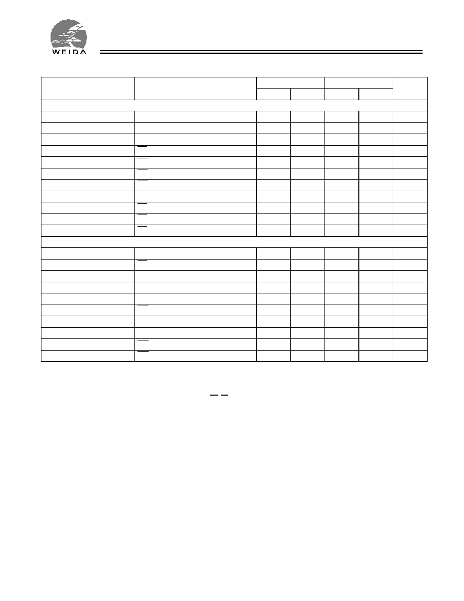
Switching Characteristics
Over the Operating Range
[5]
Parameter
Description
WCMA1008U1X-55
WCMA1008U1X-70
Unit
Min.
Max.
Min.
Max.
READ CYCLE
t
RC
Read Cycle Time
55
70
ns
t
AA
Address to Data Valid
55
70
ns
t
OHA
Data Hold from Address Change
5
10
ns
t
ACE
CE
1
LOW and CE
2
HIGH to Data Valid
55
70
ns
t
DOE
OE LOW to Data Valid
20
35
ns
t
LZOE
OE LOW to Low Z
[6]
10
10
ns
t
HZOE
OE HIGH to High Z
[6, 7]
20
25
ns
t
LZCE
CE
1
LOW and CE
2
HIGH to Low Z
[6]
10
10
ns
t
HZCE
CE
1
HIGH or CE
2
LOW to High Z
[6, 7]
20
25
ns
t
PU
CE
1
LOW and CE
2
HIGH to Power-Up
0
0
ns
t
PD
CE
1
HIGH or CE
2
LOW to Power-Down
55
70
ns
WRITE CYCLE
[8,]
t
WC
Write Cycle Time
55
70
ns
t
SCE
CE
1
LOW and CE
2
HIGH to Write End
45
60
ns
t
AW
Address Set-Up to Write End
45
60
ns
t
HA
Address Hold from Write End
0
0
ns
t
SA
Address Set-Up to Write Start
0
0
ns
t
PWE
WE Pulse Width
45
55
ns
t
SD
Data Set-Up to Write End
25
30
ns
t
HD
Data Hold from Write End
0
0
ns
t
HZWE
WE LOW to High Z
[6, 7]
20
25
ns
t
LZWE
WE HIGH to Low Z
[6]
5
5
ns
Notes:
5.
Test conditions assume signal transition time of 5 ns or less, timing reference levels of V
CC(typ.)
/2, input pulse levels of 0 to V
CC(typ.)
, and output loading of the
specified I
OL
/I
OH
and 30 pF load capacitance.
6.
At any given temperature and voltage condition, t
HZCE
is less than t
LZCE
, t
HZOE
is less than t
LZOE
, and t
HZWE
is less than t
LZWE
for any given device.
7.
t
HZOE
, t
HZCE
, and t
HZWE
transitions are measured when the outputs enter a high impedance state.
8.
The internal write time of the memory is defined by the overlap of WE, CE
1
= V
IL
and CE
2
= V
IH
. All signals must be ACTIVE to initiate a write and any of these
signals can terminate a write by going INACTIVE. The data input set-up and hold timing should be referenced to the edge of the signal that terminates the write.