128K x 16 Static RAM
WCMB2016R4X
Features
∑ Low voltage range:
-- 1.65V
-
1.95V
∑ Ultra-low active power
-- Typical Active Current: 0.5 mA @ f = 1 MHz
-- Typical Active Current: 1.5 mA @ f = f
max
∑ Low standby power
∑ Easy memory expansion with CE and OE features
∑ Automatic power-down when deselected
∑ CMOS for optimum speed/power
Functional Description
The WCMB2016R4X is a high-performance CMOS static
RAM organized as 128K words by 16 bits. This device features
advanced circuit design to provide ultra-low active current.
This device is ideal for portable applications such as cellular
telephones. The device also has an automatic power-down
feature that significantly reduces power consumption by 99%
when addresses are not toggling. The device can also be put
into standby mode when deselected (CE HIGH or both BLE
and BHE are HIGH). The input/output pins (I/O
0
through I/O
15
)
are placed in a high-impedance state when: deselected (CE
HIGH), outputs are disabled (OE HIGH), both Byte High En-
able and Byte Low Enable are disabled (BHE, BLE HIGH), or
during a write operation (CE LOW, and WE LOW).
Writing to the device is accomplished by taking Chip Enable
(CE) and Write Enable (WE) inputs LOW. If Byte Low Enable
(BLE) is LOW, then data from I/O pins (I/O
0
through I/O
7
), is
written into the location specified on the address pins (A
0
through A
16
). If Byte High Enable (BHE) is LOW, then data
from I/O pins (I/O
8
through I/O
15
) is written into the location
specified on the address pins (A
0
through A
16
).
Reading from the device is accomplished by taking Chip En-
able (CE) and Output Enable (OE) LOW while forcing the Write
Enable (WE) HIGH. If Byte Low Enable (BLE) is LOW, then
data from the memory location specified by the address pins
will appear on I/O
0
to I/O
7
. If Byte High Enable (BHE) is LOW,
then data from memory will appear on I/O
8
to I/O
15
. See the
Truth Table at the back of this data sheet for a complete de-
scription of read and write modes.
The WCMB2016R4X is available in a 48-ball FBGA package.
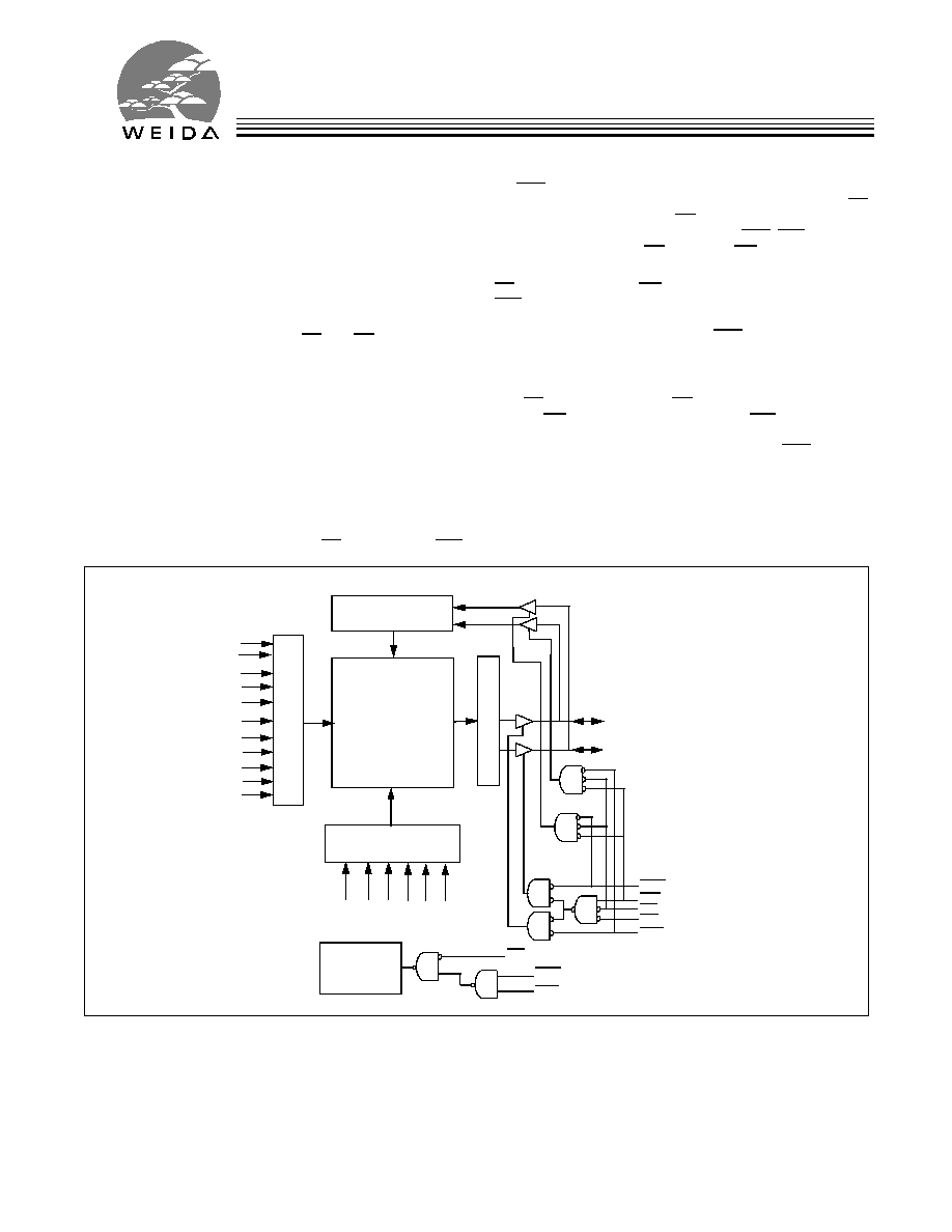
Logic Block Diagram
128K x 16
RAM Array
I/O
0
≠I/O
7
COLUMN DECODER
A
11
A
12
A
13
A
14
A
15
2048 X 1024
S
E
N
S
E AM
PS
DATA IN DRIVERS
OE
I/O
8
≠I/O
15
CE
WE
BLE
BHE
A
16
ROW
DE
CODE
R
A
7
A
6
A
3
A
0
A
2
A
1
A
5
A
4
A
8
Power - Down
Circuit
BHE
BLE
CE
A
9
A
10

2
WCMB2016R4X
Maximum Ratings
(Above which the useful life may be impaired. For user guide-
lines, not tested.)
Storage Temperature
..................................... -
65∞C to +150∞C
Ambient Temperature with
Power Applied
.................................................. -
55∞C to +125∞C
Supply Voltage to Ground Potential
.................-
0.2V to +2.4V
DC Voltage Applied to Outputs
in High Z State
[3]
........................................ -
0.2V to V
CC
+ 0.2V
DC Input Voltage
[3]
.................................... -
0.2V to V
CC
+ 0.2V
Output Current into Outputs (LOW)............................. 20 mA
Static Discharge Voltage........................................... >2001V
(per MIL-STD-883, Method 3015)
Latch-Up Current.................................................... >200 mA
Notes:
1.
NC pins are not connected to the die.
2.
E3 (DNU) can be left as NC or Vss to ensure proper application.
3.
V
IL
(min) =
-
2.0V for pulse durations less than 20 ns.
4.
Typical values are included for reference only and are not guaranteed or tested. Typical values are measured at V
CC
= V
CC(typ)
, T
A
= 25∞C.
Pin Configuration
[1, 2]
WE
V
ccq
A
11
A
10
NC
A
6
A
0
A
3
CE
I/O
10
I/O
8
I/O
9
A
4
A
5
I/O
11
I/O
13
I/O
12
I/O
14
I/O
15
V
SS
A
9
A
8
OE
V
ssq
A
7
I/O
0
BHE
NC
DNU
A
2
A
1
BLE
V
CC
I/O
2
I/O
1
I/O
3
I/O
4
I/O
5
I/O
6
I/O
7
A
15
A
14
A
13
A
12
NC
NC
NC
3
2
6
5
4
1
D
E
B
A
C
F
G
H
FBGA
A
16
Top View
Operating Range
Device
Range
Ambient Temperature
V
CC
WCMB2016R4X
Industrial
-
40∞C to +85∞C
1.65V to 1.95V
Product Portfolio
Product
V
CC
Range
Speed
Power Dissipation (Industrial)
Operating (I
CC
)
Standby (I
SB2
)
f = 1MHz
f = f
max
V
CC(min.)
V
CC(typ.)
[4]
V
CC(max.)
Typ.
[4]
Max.
Typ.
[4]
Max.
Typ.
[4]
Max.
WCMB2016R4X
1.65V
1.80V
1.95V
70 ns
0.5 mA
2 mA
1.5 mA
6 mA
1
µ
A
8
µ
A

3
WCMB2016R4X
Electrical Characteristics
Over the Operating Range
Test Conditions
WCMB2016R4X
Param-
eter
Description
Min.
Typ.
[4]
Max.
Unit
V
OH
Output HIGH Voltage
I
OH
=
-0
.1 mA
V
CC
= 1.65V
1.4
V
V
OL
Output LOW Voltage
I
OL
= 0.1 mA
V
CC
= 1.65V
0.2
V
V
IH
Input HIGH Voltage
1.4
V
CC
+ 0.2V
V
V
IL
Input LOW Voltage
-
0.2
0.4
V
I
IX
Input Leakage Current GND < V
I
< V
CC
-
1
+1
µA
I
OZ
Output Leakage Cur-
rent
GND < V
O
< V
CC
, Output Disabled
-
1
+1
µA
I
CC
V
CC
Operating Supply
Current
f = f
MAX
= 1/t
RC
V
CC
= 1.95V
I
OUT
= 0 mA
CMOS levels
1.5
6
mA
f = 1 MHz
0.5
2
mA
I
SB1
Automatic CE
Power-Down Current--
CMOS Inputs
CE > V
CC
-
0.2V,
V
IN
>Vcc-0.2V, V
IN
<0.2V
f = f
MAX
(Address and Data Only),
f=0 (OE, WE, BHE and BLE)
1
8
µA
I
SB2
Automatic CE
Power-Down Cur-
rent-- CMOS Inputs
CE > V
CC
-
0.2V
V
IN
> V
CC
-
0.2V or V
IN
< 0.2V,
f = 0, Vcc=1.95V
Capacitance
[5]
Parameter
Description
Test Conditions
Max.
Unit
C
IN
Input Capacitance
T
A
= 25∞C, f = 1 MHz,
V
CC
= V
CC(typ)
6
pF
C
OUT
Output Capacitance
8
pF
Thermal Resistance
Description
Test Conditions
Symbol
BGA
Units
Thermal Resistance (Junction
to Ambient)
[5]
Still Air, soldered on a 4.25 x 1.125 inch, 4-layer printed
circuit board
JA
55
∞
C/W
Thermal Resistance (Junction
to Case)
[5]
JC
16
∞
C/W
Note:
5.
Tested initially and after any design or process changes that may affect these parameters.

4
WCMB2016R4X
Notes:
6.
Full device operation requires linear V
CC
ramp from V
DR
to V
CC(min)
>
100
µ
s or stable at V
CC(min)
>
100
µ
s.
7.
BHE.BLE is the AND of both BHE and BLE. Chip can be deselected by either disabling the chip enable signals or by disabling both BHE and BLE.
AC Test Loads and Waveforms
V
CC
Typ
V
CC
OUTPUT
R2
30 pF
INCLUDING
JIG AND
SCOPE
GND
90%
10%
90%
10%
OUTPUT
V
Equivalent to:
TH… VENIN EQUIVALENT
ALL INPUT PULSES
RTH
R1
Rise Time:
1 V/ns
Fall Time:
1 V/ns
Parameters
1.8V
UNIT
R1
13500
Ohms
R2
10800
Ohms
R
TH
6000
Ohms
V
TH
0.80
Volts
Data Retention Characteristics
(Over the Operating Range)
Parameter
Description
Conditions
Min.
Typ.
[4]
Max.
Unit
V
DR
V
CC
for Data Retention
1.0
1.95
V
I
CCDR
Data Retention Current
V
CC
= 1.0V
CE > V
CC
-
0.2V,
V
IN
> V
CC
-
0.2V or V
IN
< 0.2V
0.5
5
µA
t
CDR
[5]
Chip Deselect to Data
Retention Time
0
ns
t
R
[6]
Operation Recovery Time
t
RC
ns
Data Retention Waveform
[7]
V
CC(min.)
V
CC(min.)
t
CDR
V
DR
> 1.0 V
DATA RETENTION MODE
t
R
CE or
V
CC
BHE.BLE

5
WCMB2016R4X
Switching Characteristics
Over the Operating Range
[8]
WCMB2016R4X
Parameter
Description
Min.
Max.
Unit
READ CYCLE
t
RC
Read Cycle Time
70
ns
t
AA
Address to Data Valid
70
ns
t
OHA
Data Hold from Address Change
10
ns
t
ACE
CE LOW to Data Valid
70
ns
t
DOE
OE LOW to Data Valid
35
ns
t
LZOE
OE LOW to Low Z
[9]
5
ns
t
HZOE
OE HIGH to High Z
[9, 10]
25
ns
t
LZCE
CE LOW to Low Z
[9]
10
ns
t
HZCE
CE HIGH to High Z
[9, 10]
25
ns
t
PU
CE LOW to Power-Up
0
ns
t
PD
CE HIGH to Power-Down
70
ns
t
DBE
BLE / BHE LOW to Data Valid
70
ns
t
LZBE
BLE / BHE LOW to Low Z
[9]
5
ns
t
HZBE
BLE / BHE HIGH to High Z
[9, 10]
25
ns
WRITE CYCLE
[11]
t
WC
Write Cycle Time
70
ns
t
SCE
CE LOW to Write End
60
ns
t
AW
Address Set-Up to Write End
60
ns
t
HA
Address Hold from Write End
0
ns
t
SA
Address Set-Up to Write Start
0
ns
t
PWE
WE Pulse Width
50
ns
t
BW
BLE / BHE LOW to Write End
60
ns
t
SD
Data Set-Up to Write End
30
ns
t
HD
Data Hold from Write End
0
ns
t
HZWE
WE LOW to High Z
[9, 10]
25
ns
t
LZWE
WE HIGH to Low Z
[9]
10
ns
Note:
8.
Test conditions assume signal transition time of 5 ns or less, timing reference levels of V
CC(typ)
/2, input pulse levels of 0 to V
CC(typ)
, and
output loading of the specified I
OL
/I
OH
and 30 pF load capacitance.
9.
At any given temperature and voltage condition, t
HZCE
is less than t
LZCE
, t
HZBE
is less than t
LZBE
, t
HZOE
is less than t
LZOE
, and t
HZWE
is less than
t
LZWE
for any given device.
10. t
HZOE
, t
HZCE
, t
HZBE
and t
HZWE
transitions are measured when the outputs enter a high impedence state.
11. The internal write time of the memory is defined by the overlap of WE, CE
= V
IL
, BHE and/or BLE =V
IL
. All signals must be ACTIVE to
initiate a write and any of these signals can terminate a write by going INACTIVE. The data input set-up and hold timing should be
referenced to the edge of the signal that terminates the write.
6
WCMB2016R4X
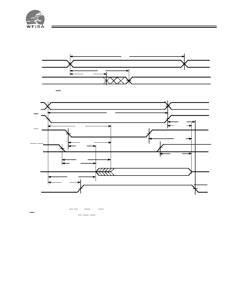
Switching Waveforms
Notes:
12. Device is continuously selected. OE, CE = V
IL
, BHE and/or BLE = V
IL.
13. WE is HIGH for read cycle.
14. Address valid prior to or coincident with CE, BHE, BLE, transition LOW.
ADDRESS
DATA OUT
PREVIOUS DATA VALID
DATA VALID
t
RC
t
AA
t
OHA
Read Cycle No. 1(Address Transition Controlled)
[12, 13]
Read Cycle No. 2 (OE Controlled)
[13, 14]
50%
50%
DATA VALID
t
RC
t
ACE
t
LZBE
t
LZCE
t
PU
DATA OUT
HIGH IMPEDANCE
IMPEDANCE
I
CC
I
SB
t
HZOE
t
HZCE
t
PD
OE
CE
HIGH
V
CC
SUPPLY
CURRENT
t
HZBE
BHE/BLE
t
LZOE
ADDRESS
t
DOE
t
DBE
7
WCMB2016R4X
Note:
15. Data I/O is high impedance if OE = V
IH
.
16. If CE goes HIGH simultaneously with WE HIGH, the output remains in a high-impedance state.
17. During this period, the I/Os are in output state and input signals should not be applied.
Switching Waveforms
t
HD
t
SD
t
PWE
t
SA
t
HA
t
AW
t
WC
DATA I/O
ADDRESS
CE
WE
OE
t
HZOE
DATA
IN
VALID
NOTE
Write Cycle No. 1 (WE Controlled)
[11, 15, 16]
17
BHE/BLE
t
BW
t
SCE
t
HD
t
SD
t
PWE
t
HA
t
AW
t
SCE
t
WC
t
HZOE
DATA
IN
VALID
CE
ADDRESS
WE
DATA I/O
OE
NOTE 17
Write Cycle No. 2 (CE
Controlled)
BHE/BLE
t
BW
[11, 15, 16]
t
SA

8
WCMB2016R4X
Switching Waveforms
DATA
IN
VALID
t
HD
t
SD
t
LZWE
t
PWE
t
SA
t
HA
t
AW
t
SCE
t
WC
t
HZWE
CE
ADDRESS
WE
DATAI/O
NOTE 17
Write Cycle No. 3 (WE Controlled, OE LOW)
t
BW
BHE/BLE
[16]
DATA I/O
ADDRESS
t
HD
t
SD
t
SA
t
HA
t
AW
t
WC
CE
WE
DATA
IN
VALID
Write Cycle No. 4 (BHE/BLE Controlled, OE LOW)
[16]
NOTE 17
t
BW
BHE/BLE
t
SCE
t
PWE

9
WCMB2016R4X
Typical DC and AC Characteristics
(
Typical values are included for reference only and are not guaranteed or tested. Typical values are measured at V
CC
= V
CC(typ)
Typ, T
A
= 25∞C.)
Truth Table
CE
WE
OE
BHE
BLE
Inputs/Outputs
Mode
Power
H
X
X
X
X
High Z
Deselect/Power-Down
Standby (I
SB
)
X
X
X
H
H
High Z
Deselect/Power-Down
Standby (I
SB
)
L
H
L
L
L
Data Out (I/O
O
≠I/O
15
)
Read
Active (I
CC
)
L
H
L
H
L
Data Out (I/O
O
≠I/O
7
);
I/O
8
≠I/O
15
in High Z
Read
Active (I
CC
)
L
H
L
L
H
Data Out (I/O
8
≠I/O
15
);
I/O
0
≠I/O
7
in High Z
Read
Active (I
CC
)
L
H
H
L
L
High Z
Output Disabled
Active (I
CC
)
L
H
H
H
L
High Z
Output Disabled
Active (I
CC
)
L
H
H
L
H
High Z
Output Disabled
Active (I
CC
)
L
L
X
L
L
Data In (I/O
O
≠I/O
15
)
Write
Active (I
CC
)
L
L
X
H
L
Data In (I/O
O
≠I/O
7
);
I/O
8
≠I/O
15
in High Z
Write
Active (I
CC
)
L
L
X
L
H
Data In (I/O
8
≠I/O
15
);
I/O
0
≠I/O
7
in High Z
Write
Active (I
CC
)
3.5
3.0
1.5
1.0
0.5
1.80
0
2.0
I
SB
(
µ
A)
2.4
2.0
1.2
0.8
0.4
1.65
1.80
1.95
0.0
1.6
I
CC
(m
A)
40
35
25
20
15
1.65
1.8
1.95
SUPPLY VOLTAGE (V)
Access Time vs. Supply Voltage
10
30
T
AA
(
n
s
)
Operating Current
Standby Current vs. Supply Voltage
SUPPLY VOLTAGE (V)
SUPPLY VOLTAGE (V)
vs. Supply Voltage
1.95
1.65
(f=f
max
)
(f = 1 MHz)

10
WCMB2016R4X
Ordering Information
Speed
(ns)
Ordering Code
Package
Name
Package Type
Operating
Range
70
WCMB2016R4X-FF70
FB48A
48-Ball Fine Pitch BGA
Industrial
Package Diagrams
48-Ball (6.0 mm x 8.0 mm x 1.0 mm) Fine Pitch BGA, FB48A
Top View
Bottom View

11
WCMB2016R4X
Document Title: WCMB2016R4X, 128K x 16 Static RAM
REV.
Spec #
ECN #
Issue Date
Orig. of Change
Description of Change
**
38-14011
115226
4/24/2002
MGN
New Data Sheet
.