
ADVANCE INFORMATION
8Mb (512K x 16) Pseudo Static RAM
WCMC8016V9X
WeidaSemiconductor, Inc.
38-14026
Revised August 2003
Features
∑ Wide voltage range: 2.70V≠3.30V
∑ Access Time: 70ns
∑ Ultra-low active power
-- Typical active current: 2.0mA @ f = 1 MHz
-- Typical active current: 11mA @ f = f
max
∑ Ultra low standby power
∑ Easy memory expansion with CE, CE
2
, and OE features
∑ Automatic power-down when deselected
∑ CMOS for optimum speed/power
∑ Offered in a 48 Ball BGA Package
Functional Description
[1]
The WCMC8016V9X is a high-performance CMOS pseudo
static RAM organized as 512K words by 16 bits that supports
an asynchronous memory interface. This device features
advanced circuit design to provide ultra-low active current.
This is ideal for providing More Battery Life
Æ
(MoBL
Æ
) in
portable applications such as cellular telephones. The device
can be put into standby mode reducing power consumption by
more than 99% when deselected using CE LOW, CE
2
HIGH
or both BHE and BLE are HIGH. The input/output pins (I/O
0
through I/O
15
) are placed in a high-impedance state when:
deselected (CE HIGH, CE
2
LOW OE is deasserted HIGH), or
during a write operation (Chip Enabled and Write Enable WE
LOW). The device also has an automatic power-down feature
that significantly reduces power consumption by 99% when
addresses are not toggling even when the chip is selected
(Chip Enable CE LOW, CE
2
HIGH and both BHE and BLE are
LOW). Reading from the device is accomplished by asserting
the Chip Enables (CE LOW and CE
2
HIGH) and Output
Enable (OE) LOW while forcing the Write Enable (WE) HIGH.
If Byte Low Enable (BLE) is LOW, then data from the memory
location specified by the address pins will appear on I/O
0
to
I/O
7
. If Byte High Enable (BHE) is LOW, then data from
memory will appear on I/O
8
to I/O
15
. See the Truth Table for a
complete description of read and write modes
Logic Block Diagram
Note:
1.
For best-practice recommendations, please refer to the Cypress application note "System Design Guidelines" on http://www.cypress .com.
512K x 16
RAM Array
I/O
0
≠I/O
7
COLUMN DECODER
S
E
N
S
E
A
M
P
S
DATA IN DRIVERS
O E
I/O
8
≠I/O
15
WE
BLE
BHE
R
O
W
D
E
C
O
D
E
R
Power
-
Down
Circuit
A
10
A
1
1
A
1
2
A
1
3
A
1
4
A
1
5
A
1
6
A
1
7
A
1
8
A
9
A
8
A
7
A
6
A
5
A
4
A
3
A
2
A
1
A
0
CE
2
CE
1T
ADVANCE INFORMATION
WCMC8016V9X
38-14026
Page - 2 - of 12
Pin Configuration
[2, 3, 4]
FBGA
Note:
2.
NC "no connect" - not connected internally to the die.
3.
DNU pins are to be left floating or tied to Vss.
4.
Ball G2 and H6 are the expansion pins for the 16Mb and 32Mb density resectively.
WE
A
11
A
10
A
6
A
0
A
3
CE
I/O
10
I/O
8
I/O
9
A
4
A
5
I/O
11
I/O
13
I/O
12
I/O
14
I/O
15
V
SS
A
9
A
8
OE
Vss
A
7
I/O
0
BHE
CE
2
A
17
A
2
A
1
BLE
V
CC
I/O
2
I/O
1
I/O
3
I/O
4
I/O
5
I/O
6
I/O
7
A
15
A
14
A
13
A
12
NC/
A
18
NC/
3
2
6
5
4
1
D
E
B
A
C
F
G
H
Top View
A
16
GND
Vcc
ADVANCE INFORMATION
WCMC8016V9X
38-14026
Page - 3 - of 12
Maximum Ratings
(Above which the useful life may be impaired. For user guide-
lines, not tested.)
Storage Temperature ................................ ≠65∞C to + 150∞C
Ambient Temperature with
Power Applied .............................................. ≠55∞C to + 85∞C
Supply Voltage to Ground Potential ................. ≠0.4V to 4.6V
DC Voltage Applied to Outputs
in High Z State
[5, 6, 7]
........................................≠0.2V to 3.3V
DC Input Voltage
[5, 6, 7]
.....................................≠0.2V to 3.3V
Output Current into Outputs (LOW).............................20 mA
Static Discharge Voltage .......................................... >2001V
(per MIL-STD-883, Method 3015)
Latch-Up Current .....................................................>200 mA
Operating Range
[9]
Device
Range
Ambient Temperature
V
CC
WCMC8016V9X
Industrial
≠25∞C to +85∞C
2.70V to 3.30V
Product Portfolio
Product
V
CC
Range (V)
Speed
(ns)
Power Dissipation
Operating I
CC
(mA)
Standby I
SB2
(
µ
A)
f = 1MHz
f = f
max
Min.
Typ.
[8]
Max.
Typ.
[8]
Max.
Typ.
[8]
Max.
Typ.
[8]
Max.
WCMC8016V9X-FI70
2.70
3.0
3.30
70
2
3.5
11
17
55
80
Notes:
5.
V
IH(MAX)
= V
CC
+ 0.5V for pulse durations less than 20ns.
6.
V
IL(MIN)
= -0.5V for pulse durations less than 20ns.
7.
Overshoot and undershoot specifications are characterized and are not 100% tested.
8.
Typical values are included for reference only and are not guranteed or tested. Typical values are measured at V
C C
= V
CC
(typ) and T
A
= 25C
9.
V
CC
must be at minimal operational levels before inputs are turned ON.

ADVANCE INFORMATION
WCMC8016V9X
38-14026
Page - 4 - of 12
Thermal Resistance
[10]
Electrical Characteristics
Over the Operating Range
Parameter
Description
Test Conditions
WCMC8016V9X-70
Unit
Min.
Typ.
[8]
Max.
V
CC
Supply Voltage
2.7
3.3
V
V
OH
Output HIGH Voltage I
OH
= ≠1.0 mA
V
CC
= 2.70V
2.4
V
V
OL
Output LOW Voltage I
OL
= 2.0mA
V
CC
= 2.70V
0.4
V
V
IH
Input HIGH Voltage
V
CC
= 2.7V to 3.3V
0.8*Vcc
V
CC
+0.3V
V
V
IL
Input LOW Voltage
V
CC
= 2.7V to 3.3V(F = 0)
-0.3
0.4
V
I
IX
Input Leakage
Current
GND < V
I
< V
CC
≠1
+1
µ
A
I
OZ
Output Leakage
Current
GND < V
O
< V
CC
, Output Disabled
≠1
+1
µ
A
I
CC
V
CC
Operating Supply
Current
f = f
MAX
= 1/t
RC
V
CC
= V
CCmax
I
OUT
= 0 mA
CMOS levels
11
17
mA
f = 1 MHz
2.0
3.5
mA
I
SB1
Automatic CE
Power-Down
Current -- CMOS
Inputs
CE > V
CC
-
0.2V or CE
2
< 0.2V
V
IN
>V
CC
≠0.2V, V
IN
<0.2V)
f = f
MAX
(Address and Data
Only),
f = 0 (OE, WE, BHE and BLE),
V
CC
=3.30V
Vcc = 3.3V
400
µ
A
I
SB2
Automatic CE
Power-Down
Current -- CMOS
Inputs
CE > V
CC
≠ 0.2V or CE
2
<
0.2V,
V
IN
> V
CC
≠ 0.2V or V
IN
< 0.2V,
f = 0, V
CC
= 3.30V
Vcc = 3.3V
55
80
µ
A
Vcc = 3.0V
50
70
µ
A
Vcc = 2.8V
45
60
µ
A
Capacitance
[10]
Parameter
Description
Test Conditions
Max.
Unit
C
IN
Input Capacitance
T
A
= 25∞C, f = 1 MHz,
V
CC
= V
CC(typ)
6
pF
C
OUT
Output Capacitance
8
pF
Description
Test Conditions
Symbol
BGA
Unit
Thermal Resistance
(Junction to Ambient)
Still Air, soldered on a 3 ◊ 4.5 inch, two-layer printed
circuit board
JA
55
∞
C/W
Thermal Resistance
(Junction to Case)
JC
16
∞
C/W
Note:
10. Tested initially and after any design or process changes that may affect these parameters.

ADVANCE INFORMATION
WCMC8016V9X
38-14026
Page - 5 - of 12
AC Test Loads and Waveforms
Parameters
3.0V V
CC
Unit
R1
1179
R2
1941
R
TH
733
V
TH
1.87
V
V
CC
V
CC
OUTPUT
R2
50 pF
INCLUDING
JIG AND
SCOPE
GND
90%
10%
90%
10%
Rise Time = 1 V/ns
Fall Time = 1 V/ns
OUTPUT
V
Equivalentto:
TH…
VENINEQUIVALENT
ALL INPUT PULSES
R
TH
R1

ADVANCE INFORMATION
WCMC8016V9X
38-14026
Page - 6 - of 12
Switching Characteristics
Over the Operating Range
[11]
Parameter
Description
70 ns
Unit
Min.
Max.
READ CYCLE
t
RC
Read Cycle Time
70
ns
t
AA
Address to Data Valid
70
ns
t
OHA
Data Hold from Address Change
10
ns
t
ACE
CE LOW and CE
2
HIGH to Data Valid
70
ns
t
DOE
OE LOW to Data Valid
35
ns
t
LZOE
OE LOW to LOW Z
[12, 14]
5
ns
t
HZOE
OE HIGH to High Z
[12, 14]
25
ns
t
LZCE
CE LOW and CE
2
HIGH to Low Z
[12, 14]
5
ns
t
HZCE
CE HIGH and CE
2
LOW to High Z
[12, 14]
25
ns
t
DBE
BLE / BHE LOW to Data Valid
70
ns
t
LZBE
BLE / BHE LOW to Low Z
[12, 14]
5
ns
t
HZBE
BLE / BHE HIGH to HIGH Z
[12, 14]
25
ns
t
SK
Address Skew
10
ns
WRITE CYCLE
[13]
t
WC
Write Cycle Time
70
ns
t
SCE
CE LOW and CE
2
HIGH
to Write End
60
ns
t
AW
Address Set-Up to Write End
60
ns
t
HA
Address Hold from Write End
0
ns
t
SA
Address Set-Up to Write Start
0
ns
t
PWE
WE Pulse Width
45
ns
t
BW
BLE / BHE LOW to Write End
60
ns
t
SD
Data Set-Up to Write End
45
ns
t
HD
Data Hold from Write End
0
ns
t
HZWE
WE LOW to High-Z
[12, 14]
25
ns
t
LZWE
WE HIGH to Low-Z
[12, 14]
5
ns
Notes:
11. Test conditions for all parameters other than tri-state parameters assume signal transition time of 1ns/V, timing reference leve ls of V
CC(typ)
/2, input pulse
levels of 0 to V
CC (typ.)
, and output loading of the specified I
OL
/I
OH
as shown in the "AC Test Loads and Waveforms" section..
12. t
HZOE
, t
HZCE
, t
HZBE
, and t
HZWE
transitions are measured when the outputs enter a high impedence state.
13. The internal Write time of the memory is defined by the overlap of WE, CE
= V
IL
, BHE and/or BLE = V
IL
, and CE
2
= V
IH
. All signals must be ACTIVE to initiate
a write and any of these signals can terminate a write by going INACTIVE. The data input set-up and hold timing should be refere nced to the edge of the
signal that terminates the write.
14. High-Z and Low-Z parameters are characterized and are not 100% tested.
ADVANCE INFORMATION
WCMC8016V9X
38-14026
Page - 7 - of 12
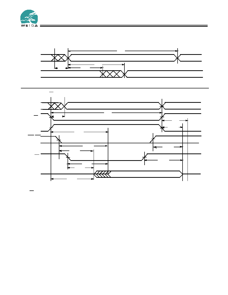
Switching Waveforms
Note:
15. WE is HIGH for read cycle.
ADDRESS
DATA OUT
PREVIOUS DATA VALID
DATA VALID
t
RC
t
AA
t
OHA
Read Cycle 1 (Address Transition Controlled)
[15]
t
SK
50%
50%
DATA VALID
t
RC
t
ACE
t
DOE
t
LZOE
t
LZCE
t
PU
HIGH IMPEDANCE
t
HZOE
t
PD
HIGH
OE
CE
I
CC
IMPEDANCE
ADDRESS
CE2
VCC
Read Cycle 2 (
O E
Controlled)
[15]
t
HZBE
BHE
/
BLE
t
LZBE
t
HZCE
DATA OUT
t
DBE
t
SK

ADVANCE INFORMATION
WCMC8016V9X
38-14026
Page - 8 - of 12
Notes:
16. Data I/O is high impedance if OE = V
IH
.
17. If Chip Enable goes INACTIVE and CE
2
goes LOW simultaneously with WE = V
IH
, the output remains in a high-impedance state.
18. During the DON'T CARE period in the DATA I/O waveform, the I/Os are in output state and input signals should not be applied.
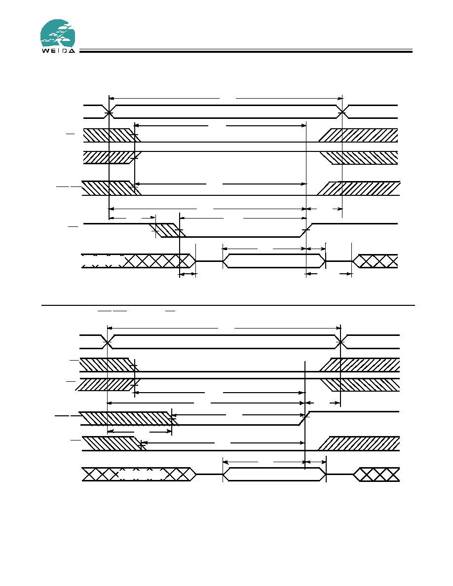
Switching Waveforms
(continued)
t
HD
t
SD
t
PWE
t
SA
t
HA
t
AW
t
SCE
t
WC
VALID DATA
CE
ADDRESS
CE2
WE
DATAI/O
OE
Write Cycle 1 (WE Controlled)
BHE
/
BLE
t
BW
[13, 14,16, 17, 18]
DON'T CARE
t
HD
t
SD
t
PWE
t
HA
t
AW
t
SCE
t
WC
t
HZOE
VALID DATA
CE
ADDRESS
CE2
WE
DATAI/O
OE
DON'T CARE
Write Cycle 2 (CE or CE
2
Controlled)
BHE /BLE
t
BW
t
SA
[13, 14,16, 17, 18]
ADVANCE INFORMATION
WCMC8016V9X
38-14026
Page - 9 - of 12
Switching Waveforms
(continued)
VALID DATA
t
HD
t
SD
t
LZWE
t
PWE
t
SA
t
HA
t
AW
t
SCE
t
WC
t
HZWE
CE
ADDRESS
CE2
WE
DATAI/O
Write Cycle 3 (WE Controlled, OE LOW)
t
BW
BHE
/
BLE
[17, 18]
DON'T CARE
DATA I/O
ADDRESS
t
HD
t
SD
t
SA
t
HA
t
AW
t
WC
CE
WE
VALID DATA
Write Cycle 4 (BHE/BLE Controlled, OE LOW)
[17, 18]
t
BW
BHE/BLE
t
SCE
CE2
t
P W E
DON'T CARE

ADVANCE INFORMATION
WCMC8016V9X
38-14026
Page - 10 - of 12
Truth Table
[19]
CE
CE
2
WE
OE
BHE
BLE
Inputs/Outputs
Mode
Power
H
X
X
X
X
X
High Z
Deselect/Power-Down
Standby (I
SB
)
X
L
X
X
X
X
High Z
Deselect/Power-Down
Standby (I
SB
)
X
X
X
X
H
H
High Z
Deselect/Power-Down
Standby (I
SB
)
L
H
H
L
L
L
Data Out (I/O0 ≠ I/O15)
Read
Active (I
CC
)
L
H
H
L
H
L
Data Out (I/O0 ≠ I/O7);
High Z (I/O8 ≠ I/O15)
Read
Active (I
CC
)
L
H
H
L
L
H
High Z (I/O0 ≠ I/O7);
Data Out (I/O8 ≠ I/O15)
Read
Active (I
CC
)
L
H
H
H
L
H
High Z
Output Disabled
Active (I
CC
)
L
H
H
H
H
L
High Z
Output Disabled
Active (I
CC
)
L
H
H
H
L
L
High Z
Output Disabled
Active (I
CC
)
L
H
L
X
L
L
Data In (I/O0 ≠ I/O15)
Write
Active (I
CC
)
L
H
L
X
H
L
Data In (I/O0 ≠ I/O7);
High Z (I/O8 ≠ I/O15)
Write
Active (I
CC
)
L
H
L
X
L
H
High Z (I/O0 ≠ I/O7);
Data In (I/O8 ≠ I/O15)
Write
Active (I
CC
)
Note:
19. H = V
I H
, L = V
IL
, X = Don't Care
Ordering Information
Speed
(ns)
Ordering Code
Package
Name
Package Type
Operating
Range
70
WCMC8016V9X-FI70
BA48K
48-ball Fine Pitch BGA (6 mm ◊ 8mm ◊ 1.2 mm)
Industrial
ADVANCE INFORMATION
WCMC8016V9X
38-14026
Page - 11 - of 12
© Weida Semiconductor, Inc., 2002. The information contained herein is subject to change without notice. Weida Semiconductor assumes no responsibility for the use of any circuitry other than
circuitry embodied in a Weida Semiconductor product. Nor does it convey or imply any license under patent or other rights. Weida Semiconductor does not authorize its products for use as
critical components in life-support systems where a malfunction or failure may reasonably be expected to result in significant injury to the user. The inclusion of Weida Semiconductor products
in life-support systems application implies that the manufacturer assumes all risk of such use and in doing so indemnifies Weida Semiconductor against all charges.
Package
MoBL and More Battery Life are trademarks of Cypress Semiconductor Corporation. All product and company names mentioned
in this document may be the trademarks of their respective holders
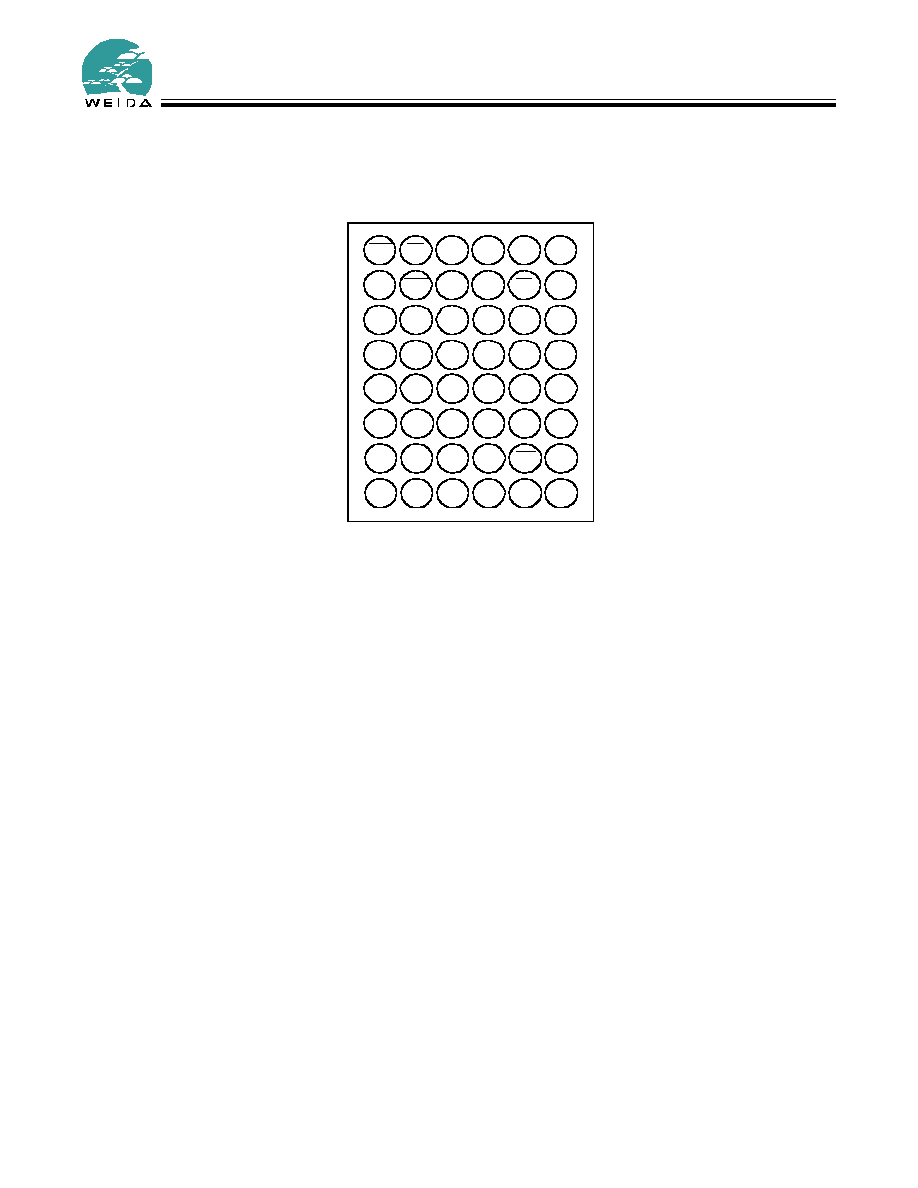
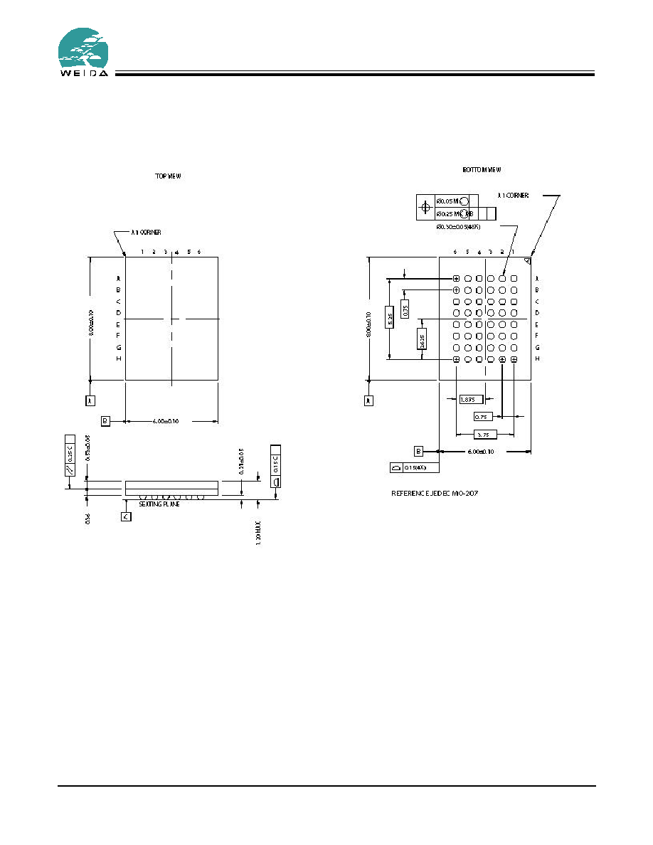
48-Ball (6 mm x 8mm x 1.2 mm) FBGA BA48K
51-85193-*A

ADVANCE INFORMATION
WCMC8016V9X
38-14026
Page - 12 - of 12
Document Title: WCMC8016V9X MoBL3
Æ
8Mb (512K x 16) Pseudo Static RAM
Document Number: 38-14026
REV.
ECN NO.
Issue
Date
Orig. of
Change
Description of Change
**
130543
10/16/03
MPR
New Datasheet