32Kx8 Static RAM
WCMS0808C1X
S0808C1X
Features
∑ Low Voltage Range
-- 4.5V≠5.5V Operation
∑ Low active power
-- 275 mW (max.)
∑ Low standby power
-- 28
µ
W (max.)
∑ Easy memory expansion with CE and OE features
∑ TTL-compatible inputs and outputs
∑ Automatic power-down when deselected
∑ CMOS for optimum speed/power
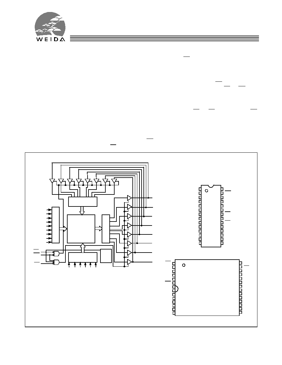
Functional Description
The WCMS0808C1X is a high-performance CMOS static
RAM organized as 32K words by 8 bits. Easy memory expan-
sion is provided by an active LOW chip enable (CE) and active
LOW output enable (OE) and three-state drivers. This device
has an automatic power-down feature, reducing the power
consumption by 99.9% when deselected. The
WCMS0808C1X is in the standard 450-mil-wide (300-mil body
width) SOIC and packages.
An active LOW write enable signal (WE) controls the writ-
ing/reading operation of the memory. When CE and WE inputs
are both LOW, data on the eight data input/output pins (I/O
0
through I/O
7
) is written into the memory location addressed by
the address present on the address pins (A
0
through A
14
).
Reading the device is accomplished by selecting the device
and enabling the outputs, CE and OE active LOW, while WE
remains inactive or HIGH. Under these conditions, the con-
tents of the location addressed by the information on address
pins are present on the eight data input/output pins.
The input/output pins remain in a high-impedance state unless
the chip is selected, outputs are enabled, and write enable
(WE) is HIGH.
Logic Block Diagram
Pin Configurations
A
9
A
8
A
7
A
6
A
5
A
4
A
3
A
2
COLUMN
DECODER
ROW
DE
CODE
R
S
E
N
S
E AM
PS
INPUTBUFFER
POWER
DOWN
WE
OE
I/O
0
CE
I/O
1
I/O
2
I/O
3
1
2
3
4
5
6
7
8
9
10
11
14
15
16
20
19
18
17
21
24
23
22
Top View
Narrow SOIC
12
13
25
28
27
26
GND
A
6
A
7
A
8
A
9
A
10
A
11
A
12
A
13
WE
V
CC
A
4
A
3
A
2
A
1
I/O
7
I/O
6
I/O
5
I/O
4
A
14
A
5
I/O
0
I/O
1
I/O
2
CE
OE
A
0
I/O
3
512x512
ARRAY
I/O
7
I/O
6
I/O
5
I/O
4
A
10
A
13
A
11
A
12
A
1
A
14
A
0
22
23
24
25
26
27
28
1
2
5
10
11
15
14
13
12
16
19
18
17
3
4
20
21
7
6
8
9
OE
A
1
A
2
A
3
A
4
WE
V
CC
A
5
A
6
A
7
A
8
A
9
A
0
CE
I/O
7
I/O
6
I/O
5
GND
I/O
2
I/O
1
I/O
4
I/O
0
A
14
A
10
A
11
A
13
A
12
I/O
3
TSOP I
Top View
(not to scale)
WCMS0808C1X
*
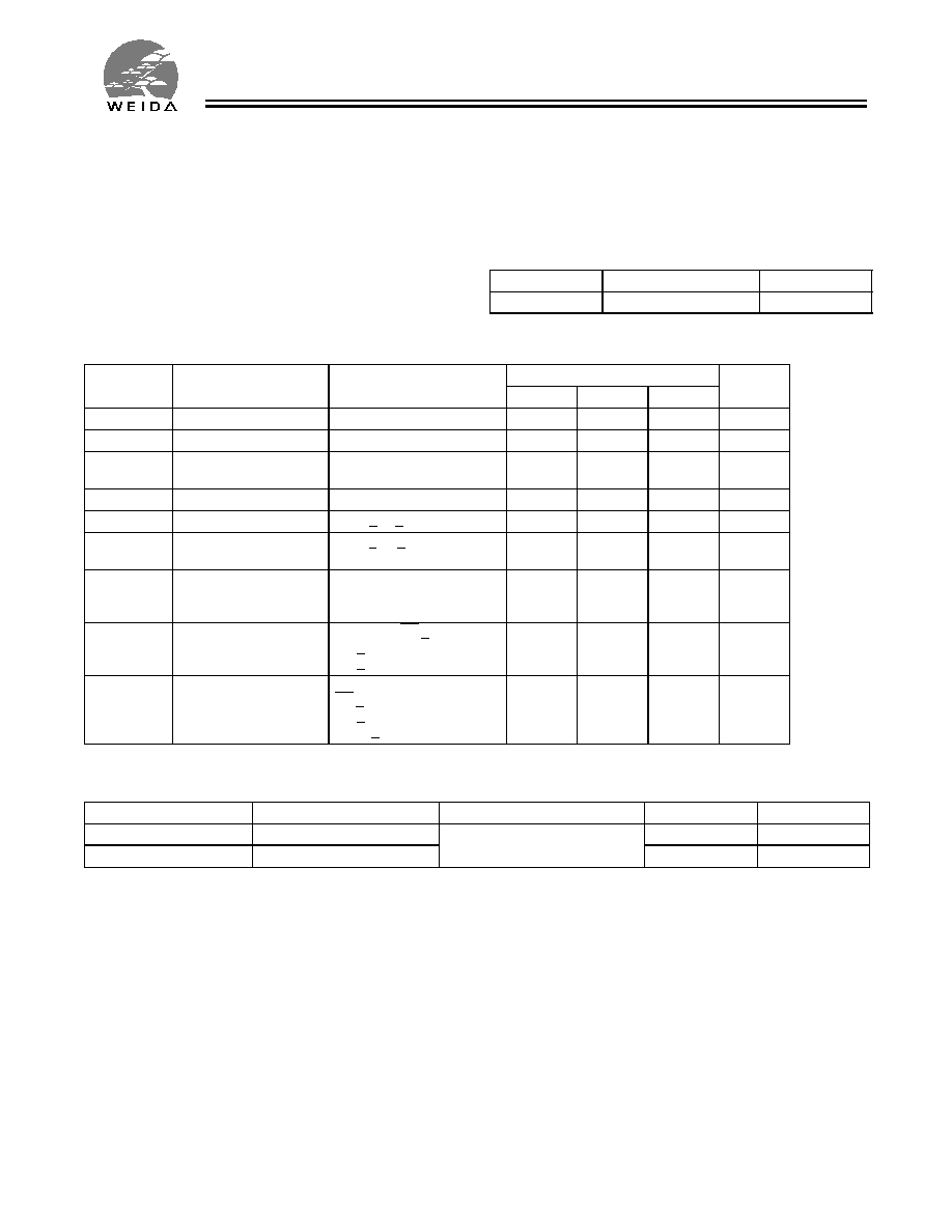
Maximum Ratings
(Above which the useful life may be impaired. For user guide-
lines, not tested.)
Storage Temperature
..................................... -
65
∞
C to +150
∞
C
Ambient Temperature with
Power Applied................................................... 0
∞
C to +70
∞
C
Supply Voltage to Ground Potential
(Pin 28 to Pin 14)
.................................................-
0.5V to +7.0V
DC Voltage Applied to Outputs
in High Z State
[1]
........................................ -
0.5V to V
CC
+ 0.5V
DC Input Voltage
[1]
.................................... -
0.5V to V
CC
+ 0.5V
Output Current into Outputs (LOW)............................. 20 mA
Static Discharge Voltage........................................... >2001V
(per MIL-STD-883, Method 3015)
Latch-Up Current.................................................... >200 mA
Operating Range
Range
Ambient Temperature
V
CC
Industrial
≠40
∞
C to +85
∞
C
5V
±
10%
Electrical Characteristics
Over the Operating Range
Parameter
Description
Test Conditions
WCMS0808C1X
Unit
Min.
Typ
[2]
Max.
V
OH
Output HIGH Voltage
V
CC
= Min., I
OH
=
-
1.0 mA
2.4
V
V
OL
Output LOW Voltage
V
CC
= Min., I
OL
= 2.1 mA
0.4
V
V
IH
Input HIGH Voltage
2.2
V
CC
+0.5V
V
V
IL
Input LOW Voltage
-
0.5
0.8
V
I
IX
Input Load Current
GND < V
I
< V
CC
-
0.5
+0.5
µ
A
I
OZ
Output Leakage
Current
GND < V
O
< V
CC
, Output Dis-
abled
-
0.5
+0.5
µ
A
I
CC
V
CC
Operating Supply
Current
V
CC
= Max.,
I
OUT
= 0 mA,
f = f
MAX
= 1/t
RC
25
50
mA
I
SB1
Automatic CE
Power-Down Current--
TTL Inputs
Max. V
CC
, CE > V
IH
,
V
IN
> V
IH
or
V
IN
< V
IL
, f = f
MAX
0.3
0.5
mA
I
SB2
Automatic CE
Power-Down Current--
CMOS Inputs
Max. V
CC
,
CE > V
CC
-
0.3V
V
IN
> V
CC
-
0.3V
or V
IN
< 0.3V, f = 0
0.1
10
µ
A
Capacitance
[3]
Parameter
Description
Test Conditions
Max.
Unit
C
IN
Input Capacitance
T
A
= 25
∞
C, f = 1 MHz,
V
CC
= 5.0V
6
pF
C
OUT
Output Capacitance
8
pF
Note:
1.
V
IL
(min.)
=
-
2.0V for pulse durations of less than 20 ns.
2.
Typical specifications are the mean values measured over a large sample size across normal production process variations and are taken at nominal conditions
(T
A
= 25
∞
C, V
CC
). Parameters are guaranteed by design and characterization, and not 100% tested.
3.
Tested initially and after any design or process changes that may affect these parameters.
WCMS0808C1X
*
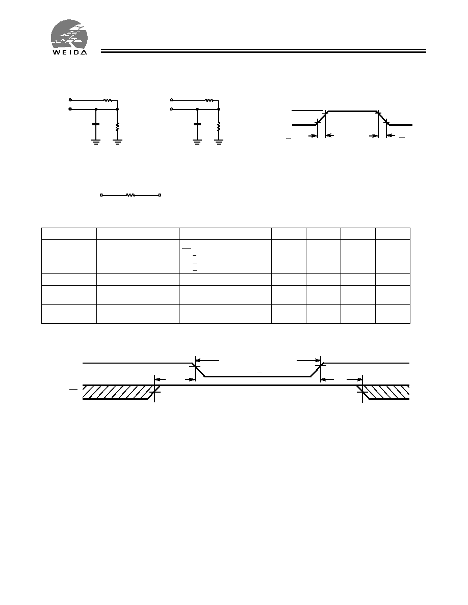
AC Test Loads and Waveforms
3.0V
5V
OUTPUT
R1 1800
R2
990
100 pF
INCLUDING
JIG AND
SCOPE
GND
90%
10%
90%
10%
< 5 ns
< 5 ns
5V
OUTPUT
R1 1800
R2
990
5 pF
INCLUDING
JIG AND
SCOPE
(a)
(b)
OUTPUT
1.77V
Equivalent to:
TH…
VENIN EQUIVALENT
ALL INPUT PULSES
639
Data Retention Characteristics
Parameter
Description
Conditions
[4]
Min.
Typ.
[2]
Max.
Unit
V
DR
V
CC
for Data Retention
V
CC
= 3.0V,
CE > V
CC
-
0.3V,
V
IN
> V
CC
-
0.3V or
V
IN
< 0.3V
2.0
V
I
CCDR
Data Retention Current
0.1
10
µ
A
t
CDR
[3]
Chip Deselect to Data
Retention Time
0
ns
t
R
[3]
Operation Recovery
Time
t
RC
ns
Data Retention Waveform
Note:
4.
No input may exceed V
CC
+0.5V.
3.0V
3.0V
t
CDR
V
DR
> 2V
DATA RETENTION MODE
t
R
CE
V
CC
WCMS0808C1X
*
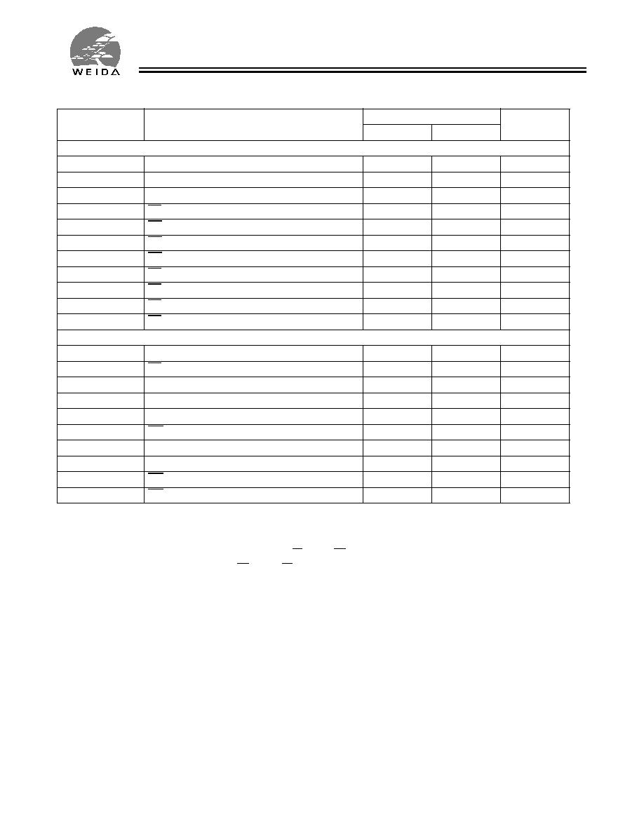
Switching Characteristics
Over the Operating Range
[10]
Parameter
Description
WCMS0808C1X
Unit
Min.
Max.
READ CYCLE
t
RC
Read Cycle Time
70
ns
t
AA
Address to Data Valid
70
ns
t
OHA
Data Hold from Address Change
5
ns
t
ACE
CE LOW to Data Valid
70
ns
t
DOE
OE LOW to Data Valid
35
ns
t
LZOE
OE LOW to Low Z
[6]
5
ns
t
HZOE
OE HIGH to High Z
[6, 7]
25
ns
t
LZCE
CE LOW to Low Z
[6]
5
ns
t
HZCE
CE HIGH to High Z
[6, 7]
25
ns
t
PU
CE LOW to Power-Up
0
ns
t
PD
CE HIGH to Power-Down
70
ns
WRITE CYCLE
[8, 9]
t
WC
Write Cycle Time
70
ns
t
SCE
CE LOW to Write End
60
ns
t
AW
Address Set-Up to Write End
60
ns
t
HA
Address Hold from Write End
0
ns
t
SA
Address Set-Up to Write Start
0
ns
t
PWE
WE Pulse Width
50
ns
t
SD
Data Set-Up to Write End
30
ns
t
HD
Data Hold from Write End
0
ns
t
HZWE
WE LOW to High Z
[6, 7]
25
ns
t
LZWE
WE HIGH to Low Z
[6]
5
ns
Notes:
5.
Test conditions assume signal transition time of 5 ns or less, timing reference levels of 1.5V, input pulse levels of 0 to 3.0V, and output loading of the
specified I
OL
/I
OH
and 100-pF load capacitance.
6.
At any given temperature and voltage condition, t
HZCE
is less than t
LZCE
, t
HZOE
is less than t
LZOE
, and t
HZWE
is less than t
LZWE
for any given device.
7.
t
HZOE
, t
HZCE
, and t
HZWE
are specified with C
L
= 5 pF as in part (b) of AC Test Loads. Transition is measured
±
500 mV from steady-state voltage.
8.
The internal write time of the memory is defined by the overlap of CE LOW and WE LOW. Both signals must be LOW to initiate a write and either signal can
terminate a write by going HIGH. The data input set-up and hold timing should be referenced to the rising edge of the signal that terminates the write.
9.
The minimum write cycle time for write cycle #3 (WE controlled, OE LOW) is the sum of t
HZWE
and t
SD

WCMS0808C1X
*
Switching Waveforms
Notes:
10. Device is continuously selected. OE, CE = V
IL
.
11. WE is HIGH for read cycle.
12. Address valid prior to or coincident with CE transition LOW.
ADDRESS
DATA OUT
PREVIOUS DATA VALID
DATA VALID
t
RC
t
AA
t
OHA
Read Cycle No. 1
[10,11]
50%
50%
DATA VALID
t
RC
t
ACE
t
DOE
t
LZOE
t
LZCE
t
PU
DATA OUT
HIGH IMPEDANCE
IMPEDANCE
ICC
ISB
t
HZOE
t
HZCE
t
PD
OE
CE
HIGH
V
CC
SUPPLY
CURRENT
Read Cycle No. 2
[11,12]

WCMS0808C1X
*
Notes:
13. Data I/O is high impedance if OE = V
IH
.
14. If CE goes HIGH simultaneously with WE HIGH, the output remains in a high-impedance state.
Switching Waveforms
(continued)
t
HD
t
SD
t
PWE
t
SA
t
HA
t
AW
t
WC
DATA I/O
ADDRESS
CE
WE
OE
t
HZOE
DATA
IN
VALID
NOTE
Write Cycle No. 1 (WE Controlled)
[8,13,14]
15
t
WC
t
AW
t
SA
t
HA
t
HD
t
SD
t
SCE
WE
DATA I/O
ADDRESS
CE
DATA
IN
VALID
Write Cycle No. 2 (CE Controlled)
[8,13,14]

WCMS0808C1X
*
Note:
15. During this period, the I/Os are in output state and input signals should not be applied.
Switching Waveforms
(continued)
DATA I/O
ADDRESS
t
HD
t
SD
t
LZWE
t
SA
t
HA
t
AW
t
WC
CE
WE
t
HZWE
DATA
IN
VALID
Write Cycle No. 3 (WE Controlled, OE LOW)
[9,14]
NOTE 15
Truth Table
CE
WE
OE
Inputs/Outputs
Mode
Power
H
X
X
High Z
Deselect/Power-Down
Standby (I
SB
)
L
H
L
Data Out
Read
Active (I
CC
)
L
L
X
Data In
Write
Active (I
CC
)
L
H
H
High Z
Deselect, Output Disabled
Active (I
CC
)
WCMS0808C1X
*
Ordering Information
Speed
(ns)
Ordering Code
Package
Name
Package Type
Operating
Range
70
WCMS0808C1X≠NF70
N28
28-Lead 450-Mil (300-Mil Body Width) Narrow SOIC
Industrial
WCMS0808C1X≠TF70
T28
28-Lead Thin Small Outiline Package (TSOP)
Package Diagrams
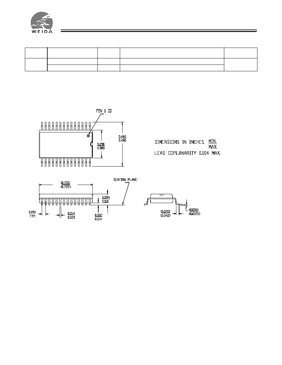
28-Lead 450-Mil (300-Mil Body Width) SOIC, N28

WCMS0808C1X
*
Package Diagrams
(continued)
28-Lead Thin Small Outline Package, T28

32Kx8 Static RAM
WCMS0808C1X
Document Title: WCMS0808C1X, 32K x 8 Static RAM
REV.
Spec #
ECN #
Issue Date
Orig. of
Change
Description
of Change
**
38-14010
115225
1/17/02
MGN
New
Datasheet