256K x 18 Synchronous
3.3V Cache RAM
WCSS0418V1F
Document #: 38-05245 Rev. **
Revised Jan 05,2002
Y7C1032
Features
∑ Supports 117-MHz microprocessor cache systems with
zero wait states
∑ 256K by 18 common I/O
∑ Fast clock-to-output times
-- 7.5 ns (117-MHz version)
∑ Two-bit wrap-around counter supporting either inter-
leaved or linear burst sequence
∑ Separate processor and controller address strobes
provide direct interface with the processor and external
cache controller
∑ Synchronous self-timed write
∑ Asynchronous output enable
∑ I/Os capable of 2.5≠3.3V operation
∑ JEDEC-standard pinout
∑ 100-pin TQFP packaging
∑ ZZ "sleep" mode
Functional Description
The WCSS0418V1F is a 3.3V, 256K by 18 synchronous cache
RAM designed to interface with high-speed microprocessors
with minimum glue logic. Maximum access delay from clock
rise is 7.5 ns (117-MHz version). A 2-bit on-chip counter cap-
tures the first address in a burst and increments the address
automatically for the rest of the burst access.
The allows WCSS0418V1F both interleaved or linear burst se-
quences, selected by the MODE input pin. A HIGH selects an
interleaved burst sequence, while a LOW selects a linear burst
sequence. Burst accesses can be initiated with the Processor
Address Strobe (ADSP) or the Cache Controller Address
Strobe (ADSC) inputs. Address advancement is controlled by
the Address Advancement (ADV) input.
A synchronous self-timed write mechanism is provided to sim-
plify the write interface. A synchronous chip enable input and
an asynchronous output enable input provide easy control for
bank selection and output three-state control.
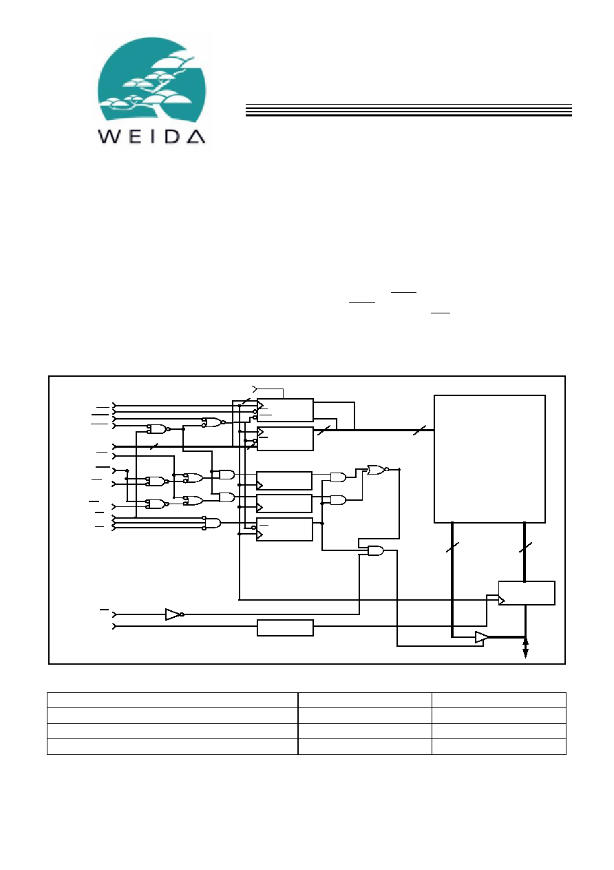
CLK
ADV
ADSC
A
[17:0]
GW
BWE
BW
0
CE
1
CE
3
CE
2
OE
ZZ
BURST
COUNTER
ADDRESS
REGISTER
INPUT
REGISTERS
256K X 18
MEMORY
ARRAY
CLK
Q
0
Q
1
Q
D
CE
CE
CLR
SLEEP
CONTROL
D
Q
DQ[15:8]
BYTEWRITE
REGISTERS
DQ[7:0]
BYTEWRITE
REGISTERS
D
Q
ENABLE
REGISTER
D
Q
CE
CLK
18
18
18
16
16
18
(A
0
,A
1
) 2
MODE
ADSP
Logic Block Diagram
DQ
[15:0]
BW
1
DP
[1:0]
Selection Guide
WCSS0418V1F-117
WCSS0418V1F-100
Maximum Access Time (ns)
7.5
8.0
Maximum Operating Current (mA)
350
325
Maximum Standby Current (mA)
10.0
10.0
Intel and Pentium are registered trademarks of Intel Corporation.
WCSS0418V1F
Document #: 38-05245 Rev. **
Page 2 of 18
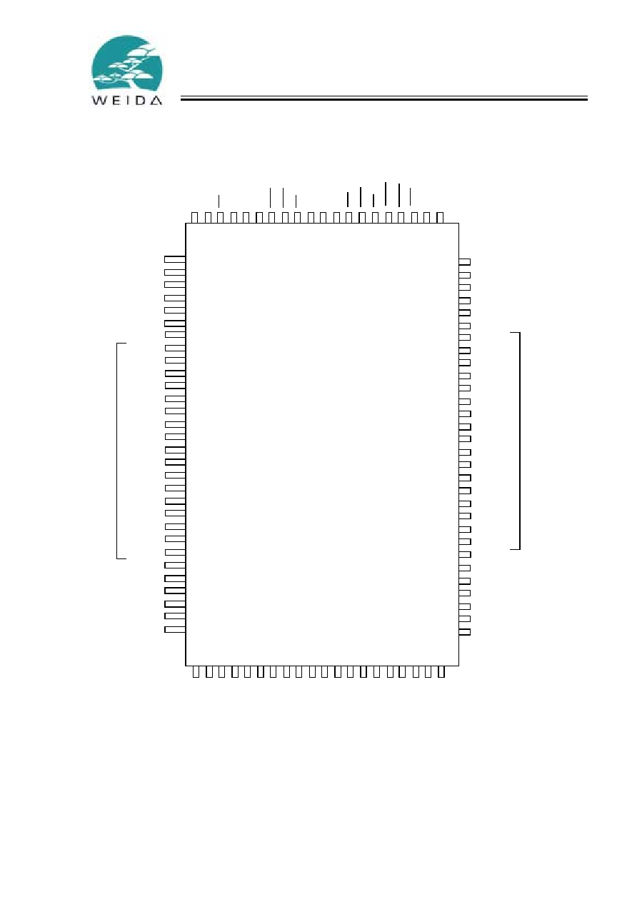
Pin Configurations
A
5
A
4
A
3
A
2
A
1
A
0
DNU
DNU
V
SS
V
DD
DNU
A
11
A
12
A
13
A
14
A
15
A
17
A
10
NC
NC
V
DDQ
V
SS
NC
DP
0
DQ
7
DQ
6
V
SS
V
DDQ
DQ
5
DQ
4
V
SS
NC
V
DD
DQ
3
DQ
2
V
DDQ
V
SS
DQ
1
DQ
0
NC
NC
V
SS
V
DDQ
NC
NC
NC
NC
NC
NC
V
DDQ
V
SS
NC
NC
DQ
8
DQ
9
V
SS
V
DDQ
DQ
10
DQ
11
NC
V
DD
NC
V
SS
DQ
12
DQ
13
V
DDQ
V
SS
DQ
14
DQ
15
DP
1
NC
V
SS
V
DDQ
NC
NC
NC
A6
A7
CE
1
CE
2
NC
NC
BWS
1
BWS
0
CE
3
V
DD
V
SS
CLK
GW
BWE
OE
AD
S
P
A
8
A
9
1
2
3
4
5
6
7
8
9
10
11
12
13
14
15
16
17
18
19
20
21
22
23
24
25
26
27
28
29
30
31
32
33
34
35
36
37
38
39
40
41
42
43
44
45
46
47
48
49
50
80
79
78
77
76
75
74
73
72
71
70
69
68
67
66
65
64
63
62
61
60
59
58
57
56
55
54
53
52
51
10
0
99
98
97
96
95
94
93
92
91
90
89
88
87
86
85
84
83
82
81
BYTE0
BYTE1
A
16
AD
V
AD
S
C
ZZ
MO
DE
DNU
WCSS0418V1F
100-Lead TQFP
WCSS0418V1F
Document #: 38-05245 Rev. **
Page 3 of 18
Pin Configurations
(continued)
2
3
4
5
6
7
1
A
B
C
D
E
F
G
H
J
K
L
M
N
P
R
T
U
V
DDQ
NC
NC
NC
DQ
b
DQ
b
DQ
b
DQ
b
A
A
A
A
ADSP
V
DDQ
CE
2
A
NC
V
DDQ
NC
V
DDQ
V
DDQ
V
DDQ
NC
NC
NC
NC
V
DDQ
V
DD
CLK
V
DD
V
SS
V
SS
V
SS
V
SS
V
SS
V
SS
V
SS
V
SS
NC
NC
NC
V
SS
NC
NC
NC
NC
A
A
NC
V
DDQ
V
DDQ
V
DDQ
A
NC
A
A
CE
3
A
A
A
A
A
A
A0
A1
DQ
a
DQ
b
NC
NC
DQ
a
NC
DQ
a
DQ
a
NC
NC
DQ
a
NC
DQ
a
NC
DQ
a
NC
DQ
a
V
DD
NC
DQ
b
NC
V
DD
DQ
b
NC
DQ
b
NC
ADSC
NC
CE
1
OE
ADV
GW
V
SS
V
SS
V
SS
V
SS
V
SS
V
SS
V
SS
V
SS
NC
MODE
DQP
b
DQP
a
V
ss
BW
b
NC
V
DD
NC
BW
a
NC
BWE
V
ss
ZZ
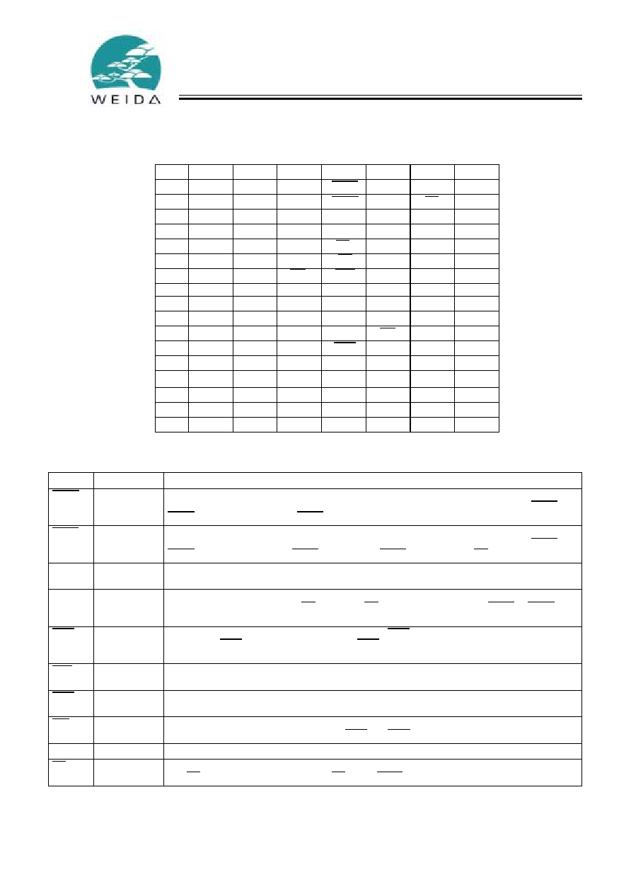
119-Ball BGA
A
Pin Descriptions
Name
I/O
Description
ADSC
Input-
Synchronous
Address Strobe from Controller, sampled on the rising edge of CLK. When asserted LOW, A
[17:0]
is captured in the address registers. A
[1:0]
are also loaded into the burst counter. When ADSP and
ADSC are both asserted, only ADSP is recognized.
ADSP
Input-
Synchronous
Address Strobe from Processor, sampled on the rising edge of CLK. When asserted LOW, A
[17:0]
is captured in the address registers. A
[1:0]
are also loaded into the burst counter. When ADSP and
ADSC are both asserted, only ADSP is recognized. ASDP is ignored when CE
1
is deasserted HIGH.
A
[1:0]
Input-
Synchronous
A
1
, A
0
address inputs, These inputs feed the on-chip burst counter as the LSBs as well as being
used to access a particular memory location in the memory array.
A
[17:2]
Input-
Synchronous
Address Inputs used in conjunction with A
[1:0]
to select one of the 256K address locations. Sampled
at the rising edge of the CLK, if CE
1
,
CE
2
,
and CE
3
are sampled active, and ADSP or ADSC is
active LOW.
BWS
[1:0]
Input-
Synchronous
Byte Write Select Inputs, active LOW. Qualified with BWE to conduct byte writes. Sampled on the
rising edge. BWS
0
controls DQ
[7:0]
and DP
0
, BWS
1
controls DQ
[15:8]
and DP
1
. See Write Cycle
Descriptions table for further details.
ADV
Input-
Synchronous
Advance input used to advance the on-chip address counter. When LOW the internal burst counter
is advanced in a burst sequence. The burst sequence is selected using the MODE input.
BWE
Input-
Synchronous
Byte Write Enable Input, active LOW. Sampled on the rising edge of CLK. This signal must be
asserted LOW to conduct a byte write.
GW
Input-
Synchronous
Global Write Input, active LOW. Sampled on the rising edge of CLK. This signal is used to conduct
a global write, independent of the state of BWE and BWS
[1:0]
. Global writes override byte writes.
CLK
Input-Clock
Clock input. Used to capture all synchronous inputs to the device.
CE
1
Input-
Synchronous
Chip Enable 1 Input, active LOW. Sampled on the rising edge of CLK. Used in conjunction with CE
2
and CE
3
to select/deselect the device. CE
1
gates ADSP.
WCSS0418V1F
Document #: 38-05245 Rev. **
Page 4 of 18
Functional Overview
All synchronous inputs pass through input registers controlled
by the rising edge of the clock. Maximum access delay from
the clock rise (t
CDV
) is 7.5 ns (117-MHz device).
The WCSS0418V1F supports secondary cache in systems
utilizing either a linear or interleaved burst sequence. The in-
terleaved burst order supports Pentium and i486 processors.
The linear burst sequence is suited for processors that utilize
a linear burst sequence. The burst order is user selectable,
and is determined by sampling the MODE input. Accesses can
be initiated with either the Processor Address Strobe (ADSP)
or the Controller Address Strobe (ADSC). Address advance-
ment through the burst sequence is controlled by the ADV in-
put. A two-bit on-chip wraparound burst counter captures the
first address in a burst sequence and automatically increments
the address for the rest of the burst access.
Byte write operations are qualified with the Byte Write Enable
(BWE) and Byte Write Select (BW
[3:0]
) inputs. A Global Write
Enable (GW) overrides all byte write inputs and writes data to
all four bytes. All writes are simplified with on-chip synchro-
nous self-timed write circuitry.
Three synchronous Chip Selects (CE
1
, CE
2
, CE
3
) and an
asynchronous Output Enable (OE) provide for easy bank se-
lection and output three-state control. ADSP is ignored if CE
1
is HIGH.
Single Read Accesses
A single read access is initiated when the following conditions
are satisfied at clock rise: (1) CE
1
, CE
2
, and CE
3
are all as-
serted active, and (2) ADSP or ADSC is asserted LOW (if the
access is initiated by ADSC, the write inputs must be deassert-
ed during this first cycle). The address presented to the ad-
dress inputs is latched into the address register and the burst
counter/control logic and presented to the memory core. If the
OE input is asserted LOW, the requested data will be available
at the data outputs a maximum to t
CDV
after clock rise. ADSP
is ignored if CE
1
is HIGH.
Single Write Accesses Initiated by ADSP
This access is initiated when the following conditions are sat-
isfied at clock rise: (1) CE
1
, CE
2
, and CE
3
are all asserted
active, and (2) ADSP is asserted LOW. The addresses pre-
sented are loaded into the address register and the burst
counter/control logic and delivered to the RAM core. The write
inputs (GW, BWE, and BWS
[1:0]
) are ignored during this first
clock cycle. If the write inputs are asserted active (see Write
Cycle Descriptions table for appropriate states that indicate a
write) on the next clock rise, the appropriate data will be
latched and written into the device. Byte writes are allowed.
During byte writes, BWS
0
controls DQ
[7:0]
and DP
0
while
BWS
1
controls DQ
[15:8]
and DP
1
. All I/Os are three-stated dur-
ing a byte write. Since these are common I/O devices, the
asynchronous OE input signal must be deasserted and the
CE
2
Input-
Synchronous
Chip Enable 2 Input, active HIGH. Sampled on the rising edge of CLK. Used in conjunction with
CE
1
and CE
3
to select/deselect the device.
CE
3
Input-
Synchronous
Chip Enable 3 Input, active LOW. Sampled on the rising edge of CLK. Used in conjunction with CE
1
and CE
2
to select/deselect the device.
OE
Input-
Asynchronous
Output Enable, asynchronous input, active LOW. Controls the direction of the I/O pins. When LOW,
the I/O pins behave as outputs. When deasserted HIGH, I/O pins are three-stated, and act as input
data pins.
ZZ
Input-
Asynchronous
Snooze Input. Active HIGH asynchronous. When HIGH, the device enters a low-power standby
mode in which all other inputs are ignored, but the data in the memory array is maintained. Leaving
ZZ floating or NC will default the device into an active state. ZZ pin has an internal pull-down.
MODE
-
Mode Input. Selects the burst order of the device. Tied HIGH selects the interleaved burst order.
Pulled LOW selects the linear burst order. When left floating or NC, defaults to interleaved burst
order. Mode pin has an internal pull-up.
DQ
[15:0]
I/O-
Synchronous
Bidirectional Data I/O lines. As inputs, they feed into an on-chip data register that is triggered by
the rising edge of CLK. As outputs, they deliver the data contained in the memory location specified
by A
[17:0]
during the previous clock rise of the read cycle. The direction of the pins is controlled by
OE in conjunction with the internal control logic. When OE is asserted LOW, the pins behave as
outputs. When HIGH, DQ
[15:0]
and DP
[1:0]
are placed in a three-state condition. The outputs are
automatically three-stated when a WRITE cycle is detected.
DP
[1:0]
I/O-
Synchronous
Bidirectional Data Parity lines. These behave identical to DQ
[15:0]
described above. These signals
can be used as parity bits for bytes 0 and 1 respectively.
V
DD
Power Supply Power supply inputs to the core of the device. Should be connected to 3.3V power supply.
V
SS
Ground
Ground for the device. Should be connected to ground of the system.
V
DDQ
I/O Power
Supply
Power supply for the I/O circuitry. Should be connected to a 2.5 or 3.3V power supply.
NC
-
No connects.
DNU
-
Do not use pins. Should be left unconnected or tied LOW.
Pin Descriptions
(continued)
Name
I/O
Description
WCSS0418V1F
Document #: 38-05245 Rev. **
Page 5 of 18
I/Os must be three-stated prior to the presentation of data to
DQ
[15:0]
and DP
[1:0]
. As a safety precaution, the data lines are
three-stated once a write cycle is detected, regardless of the
state of OE.
Single Write Accesses Initiated by ADSC
This write access is initiated when the following conditions are
satisfied at clock rise: (1) CE
1
, CE
2
, and CE
3
are all asserted
active, (2) ADSC is asserted LOW, (3) ADSP is deasserted
HIGH, and (4) the write input signals (GW, BWE, and BWS
[1:0]
)
indicate a write access. ADSC is ignored if ADSP is active LOW.
The addresses presented are loaded into the address register,
burst counter/control logic and delivered to the RAM core. The
information presented to DQ
[15:0]
and DP
[1:0]
will be written
into the specified address location. Byte writes are allowed,
with BWS
0
controlling DQ
[7:0]
and DP
0
while BWS
1
controlling
DQ
[15:8]
and DP
1
. All I/Os are three-stated when a write is
detected, even a byte write. Since these are common I/O de-
vices, the asynchronous OE input signal must be deasserted
and the I/Os must be three-stated prior to the presentation of
data to DQ
[15:0]
and DP
[1:0]
. As a safety precaution, the data
lines are three-stated once a write cycle is detected, regard-
less of the state of OE.
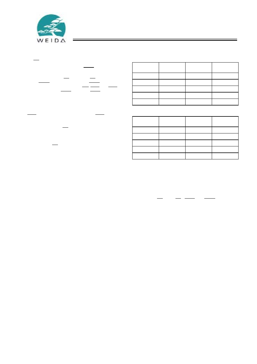
Burst Sequences
This family of devices provides a 2-bit wrap-around burst
counter inside the SRAM. The burst counter is fed by A
[1:0]
,
and can follow either a linear or interleaved burst order. The
burst order is determined by the state of the MODE input. A
LOW on MODE will select a linear burst sequence. A HIGH on
MODE will select an interleaved burst order. Leaving MODE
unconnected will cause the device to default to an interleaved
burst sequence.
Sleep Mode
The ZZ input pin is an asynchronous input. Asserting ZZ HIGH
places the SRAM in a power conservation "sleep" mode. Two
clock cycles are required to enter into or exit from this "sleep"
mode. While in this mode, data integrity is guaranteed. Ac-
cesses pending when entering the "sleep" mode are not con-
sidered valid nor is the completion of the operation guaran-
teed. The device must be deselected prior to entering the
"sleep" mode. CE
1
, CE
2
, CE
3
, ADSP, and ADSC must remain
inactive for the duration of t
ZZREC
after the ZZ input returns
LOW.
Table 1. Counter Implementation for the IntelÆ
PentiumÆ/80486 Processor's Sequence
First
Address
Second
Address
Third
Address
Fourth
Address
A
X + 1
,
A
x
A
X + 1
,
A
x
A
X + 1
,
A
x
A
X + 1
,
A
x
00
01
10
11
01
00
11
10
10
11
00
01
11
10
01
00
Table 2. Counter Implementation for a Linear Sequence
First
Address
Second
Address
Third
Address
Fourth
Address
A
X + 1
, A
x
A
X + 1
, A
x
A
X + 1
, A
x
A
X + 1
, A
x
00
01
10
11
01
10
11
00
10
11
00
01
11
00
01
10