
256K x 18 Synchronous
3.3V Cache RAM
WCSS0418V1F
Document #: 38-05245 Rev. **
Revised Jan 05,2002
Y7C1032
Features
∑ Supports 117-MHz microprocessor cache systems with
zero wait states
∑ 256K by 18 common I/O
∑ Fast clock-to-output times
-- 7.5 ns (117-MHz version)
∑ Two-bit wrap-around counter supporting either inter-
leaved or linear burst sequence
∑ Separate processor and controller address strobes
provide direct interface with the processor and external
cache controller
∑ Synchronous self-timed write
∑ Asynchronous output enable
∑ I/Os capable of 2.5≠3.3V operation
∑ JEDEC-standard pinout
∑ 100-pin TQFP packaging
∑ ZZ "sleep" mode
Functional Description
The WCSS0418V1F is a 3.3V, 256K by 18 synchronous cache
RAM designed to interface with high-speed microprocessors
with minimum glue logic. Maximum access delay from clock
rise is 7.5 ns (117-MHz version). A 2-bit on-chip counter cap-
tures the first address in a burst and increments the address
automatically for the rest of the burst access.
The allows WCSS0418V1F both interleaved or linear burst se-
quences, selected by the MODE input pin. A HIGH selects an
interleaved burst sequence, while a LOW selects a linear burst
sequence. Burst accesses can be initiated with the Processor
Address Strobe (ADSP) or the Cache Controller Address
Strobe (ADSC) inputs. Address advancement is controlled by
the Address Advancement (ADV) input.
A synchronous self-timed write mechanism is provided to sim-
plify the write interface. A synchronous chip enable input and
an asynchronous output enable input provide easy control for
bank selection and output three-state control.
CLK
ADV
ADSC
A
[17:0]
GW
BWE
BW
0
CE
1
CE
3
CE
2
OE
ZZ
BURST
COUNTER
ADDRESS
REGISTER
INPUT
REGISTERS
256K X 18
MEMORY
ARRAY
CLK
Q
0
Q
1
Q
D
CE
CE
CLR
SLEEP
CONTROL
D
Q
DQ[15:8]
BYTEWRITE
REGISTERS
DQ[7:0]
BYTEWRITE
REGISTERS
D
Q
ENABLE
REGISTER
D
Q
CE
CLK
18
18
18
16
16
18
(A
0
,A
1
) 2
MODE
ADSP
Logic Block Diagram
DQ
[15:0]
BW
1
DP
[1:0]
Selection Guide
WCSS0418V1F-117
WCSS0418V1F-100
Maximum Access Time (ns)
7.5
8.0
Maximum Operating Current (mA)
350
325
Maximum Standby Current (mA)
10.0
10.0
Intel and Pentium are registered trademarks of Intel Corporation.
WCSS0418V1F
Document #: 38-05245 Rev. **
Page 2 of 18
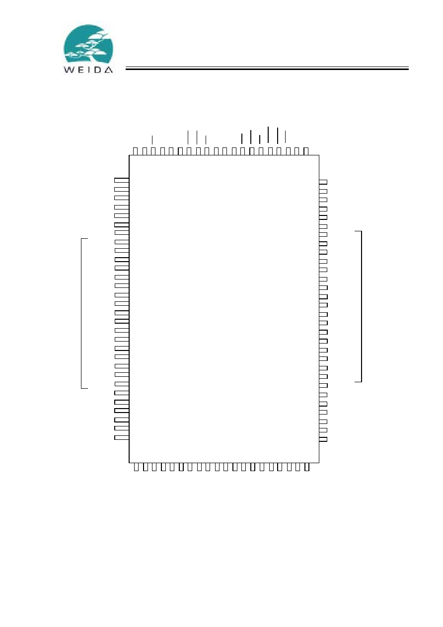
Pin Configurations
A
5
A
4
A
3
A
2
A
1
A
0
DNU
DNU
V
SS
V
DD
DNU
A
11
A
12
A
13
A
14
A
15
A
17
A
10
NC
NC
V
DDQ
V
SS
NC
DP
0
DQ
7
DQ
6
V
SS
V
DDQ
DQ
5
DQ
4
V
SS
NC
V
DD
DQ
3
DQ
2
V
DDQ
V
SS
DQ
1
DQ
0
NC
NC
V
SS
V
DDQ
NC
NC
NC
NC
NC
NC
V
DDQ
V
SS
NC
NC
DQ
8
DQ
9
V
SS
V
DDQ
DQ
10
DQ
11
NC
V
DD
NC
V
SS
DQ
12
DQ
13
V
DDQ
V
SS
DQ
14
DQ
15
DP
1
NC
V
SS
V
DDQ
NC
NC
NC
A6
A7
CE
1
CE
2
NC
NC
BWS
1
BWS
0
CE
3
V
DD
V
SS
CLK
GW
BWE
OE
AD
S
P
A
8
A
9
1
2
3
4
5
6
7
8
9
10
11
12
13
14
15
16
17
18
19
20
21
22
23
24
25
26
27
28
29
30
31
32
33
34
35
36
37
38
39
40
41
42
43
44
45
46
47
48
49
50
80
79
78
77
76
75
74
73
72
71
70
69
68
67
66
65
64
63
62
61
60
59
58
57
56
55
54
53
52
51
10
0
99
98
97
96
95
94
93
92
91
90
89
88
87
86
85
84
83
82
81
BYTE0
BYTE1
A
16
AD
V
AD
S
C
ZZ
MO
DE
DNU
WCSS0418V1F
100-Lead TQFP
WCSS0418V1F
Document #: 38-05245 Rev. **
Page 3 of 18
Pin Configurations
(continued)
2
3
4
5
6
7
1
A
B
C
D
E
F
G
H
J
K
L
M
N
P
R
T
U
V
DDQ
NC
NC
NC
DQ
b
DQ
b
DQ
b
DQ
b
A
A
A
A
ADSP
V
DDQ
CE
2
A
NC
V
DDQ
NC
V
DDQ
V
DDQ
V
DDQ
NC
NC
NC
NC
V
DDQ
V
DD
CLK
V
DD
V
SS
V
SS
V
SS
V
SS
V
SS
V
SS
V
SS
V
SS
NC
NC
NC
V
SS
NC
NC
NC
NC
A
A
NC
V
DDQ
V
DDQ
V
DDQ
A
NC
A
A
CE
3
A
A
A
A
A
A
A0
A1
DQ
a
DQ
b
NC
NC
DQ
a
NC
DQ
a
DQ
a
NC
NC
DQ
a
NC
DQ
a
NC
DQ
a
NC
DQ
a
V
DD
NC
DQ
b
NC
V
DD
DQ
b
NC
DQ
b
NC
ADSC
NC
CE
1
OE
ADV
GW
V
SS
V
SS
V
SS
V
SS
V
SS
V
SS
V
SS
V
SS
NC
MODE
DQP
b
DQP
a
V
ss
BW
b
NC
V
DD
NC
BW
a
NC
BWE
V
ss
ZZ
119-Ball BGA
A
Pin Descriptions
Name
I/O
Description
ADSC
Input-
Synchronous
Address Strobe from Controller, sampled on the rising edge of CLK. When asserted LOW, A
[17:0]
is captured in the address registers. A
[1:0]
are also loaded into the burst counter. When ADSP and
ADSC are both asserted, only ADSP is recognized.
ADSP
Input-
Synchronous
Address Strobe from Processor, sampled on the rising edge of CLK. When asserted LOW, A
[17:0]
is captured in the address registers. A
[1:0]
are also loaded into the burst counter. When ADSP and
ADSC are both asserted, only ADSP is recognized. ASDP is ignored when CE
1
is deasserted HIGH.
A
[1:0]
Input-
Synchronous
A
1
, A
0
address inputs, These inputs feed the on-chip burst counter as the LSBs as well as being
used to access a particular memory location in the memory array.
A
[17:2]
Input-
Synchronous
Address Inputs used in conjunction with A
[1:0]
to select one of the 256K address locations. Sampled
at the rising edge of the CLK, if CE
1
,
CE
2
,
and CE
3
are sampled active, and ADSP or ADSC is
active LOW.
BWS
[1:0]
Input-
Synchronous
Byte Write Select Inputs, active LOW. Qualified with BWE to conduct byte writes. Sampled on the
rising edge. BWS
0
controls DQ
[7:0]
and DP
0
, BWS
1
controls DQ
[15:8]
and DP
1
. See Write Cycle
Descriptions table for further details.
ADV
Input-
Synchronous
Advance input used to advance the on-chip address counter. When LOW the internal burst counter
is advanced in a burst sequence. The burst sequence is selected using the MODE input.
BWE
Input-
Synchronous
Byte Write Enable Input, active LOW. Sampled on the rising edge of CLK. This signal must be
asserted LOW to conduct a byte write.
GW
Input-
Synchronous
Global Write Input, active LOW. Sampled on the rising edge of CLK. This signal is used to conduct
a global write, independent of the state of BWE and BWS
[1:0]
. Global writes override byte writes.
CLK
Input-Clock
Clock input. Used to capture all synchronous inputs to the device.
CE
1
Input-
Synchronous
Chip Enable 1 Input, active LOW. Sampled on the rising edge of CLK. Used in conjunction with CE
2
and CE
3
to select/deselect the device. CE
1
gates ADSP.

WCSS0418V1F
Document #: 38-05245 Rev. **
Page 4 of 18
Functional Overview
All synchronous inputs pass through input registers controlled
by the rising edge of the clock. Maximum access delay from
the clock rise (t
CDV
) is 7.5 ns (117-MHz device).
The WCSS0418V1F supports secondary cache in systems
utilizing either a linear or interleaved burst sequence. The in-
terleaved burst order supports Pentium and i486 processors.
The linear burst sequence is suited for processors that utilize
a linear burst sequence. The burst order is user selectable,
and is determined by sampling the MODE input. Accesses can
be initiated with either the Processor Address Strobe (ADSP)
or the Controller Address Strobe (ADSC). Address advance-
ment through the burst sequence is controlled by the ADV in-
put. A two-bit on-chip wraparound burst counter captures the
first address in a burst sequence and automatically increments
the address for the rest of the burst access.
Byte write operations are qualified with the Byte Write Enable
(BWE) and Byte Write Select (BW
[3:0]
) inputs. A Global Write
Enable (GW) overrides all byte write inputs and writes data to
all four bytes. All writes are simplified with on-chip synchro-
nous self-timed write circuitry.
Three synchronous Chip Selects (CE
1
, CE
2
, CE
3
) and an
asynchronous Output Enable (OE) provide for easy bank se-
lection and output three-state control. ADSP is ignored if CE
1
is HIGH.
Single Read Accesses
A single read access is initiated when the following conditions
are satisfied at clock rise: (1) CE
1
, CE
2
, and CE
3
are all as-
serted active, and (2) ADSP or ADSC is asserted LOW (if the
access is initiated by ADSC, the write inputs must be deassert-
ed during this first cycle). The address presented to the ad-
dress inputs is latched into the address register and the burst
counter/control logic and presented to the memory core. If the
OE input is asserted LOW, the requested data will be available
at the data outputs a maximum to t
CDV
after clock rise. ADSP
is ignored if CE
1
is HIGH.
Single Write Accesses Initiated by ADSP
This access is initiated when the following conditions are sat-
isfied at clock rise: (1) CE
1
, CE
2
, and CE
3
are all asserted
active, and (2) ADSP is asserted LOW. The addresses pre-
sented are loaded into the address register and the burst
counter/control logic and delivered to the RAM core. The write
inputs (GW, BWE, and BWS
[1:0]
) are ignored during this first
clock cycle. If the write inputs are asserted active (see Write
Cycle Descriptions table for appropriate states that indicate a
write) on the next clock rise, the appropriate data will be
latched and written into the device. Byte writes are allowed.
During byte writes, BWS
0
controls DQ
[7:0]
and DP
0
while
BWS
1
controls DQ
[15:8]
and DP
1
. All I/Os are three-stated dur-
ing a byte write. Since these are common I/O devices, the
asynchronous OE input signal must be deasserted and the
CE
2
Input-
Synchronous
Chip Enable 2 Input, active HIGH. Sampled on the rising edge of CLK. Used in conjunction with
CE
1
and CE
3
to select/deselect the device.
CE
3
Input-
Synchronous
Chip Enable 3 Input, active LOW. Sampled on the rising edge of CLK. Used in conjunction with CE
1
and CE
2
to select/deselect the device.
OE
Input-
Asynchronous
Output Enable, asynchronous input, active LOW. Controls the direction of the I/O pins. When LOW,
the I/O pins behave as outputs. When deasserted HIGH, I/O pins are three-stated, and act as input
data pins.
ZZ
Input-
Asynchronous
Snooze Input. Active HIGH asynchronous. When HIGH, the device enters a low-power standby
mode in which all other inputs are ignored, but the data in the memory array is maintained. Leaving
ZZ floating or NC will default the device into an active state. ZZ pin has an internal pull-down.
MODE
-
Mode Input. Selects the burst order of the device. Tied HIGH selects the interleaved burst order.
Pulled LOW selects the linear burst order. When left floating or NC, defaults to interleaved burst
order. Mode pin has an internal pull-up.
DQ
[15:0]
I/O-
Synchronous
Bidirectional Data I/O lines. As inputs, they feed into an on-chip data register that is triggered by
the rising edge of CLK. As outputs, they deliver the data contained in the memory location specified
by A
[17:0]
during the previous clock rise of the read cycle. The direction of the pins is controlled by
OE in conjunction with the internal control logic. When OE is asserted LOW, the pins behave as
outputs. When HIGH, DQ
[15:0]
and DP
[1:0]
are placed in a three-state condition. The outputs are
automatically three-stated when a WRITE cycle is detected.
DP
[1:0]
I/O-
Synchronous
Bidirectional Data Parity lines. These behave identical to DQ
[15:0]
described above. These signals
can be used as parity bits for bytes 0 and 1 respectively.
V
DD
Power Supply Power supply inputs to the core of the device. Should be connected to 3.3V power supply.
V
SS
Ground
Ground for the device. Should be connected to ground of the system.
V
DDQ
I/O Power
Supply
Power supply for the I/O circuitry. Should be connected to a 2.5 or 3.3V power supply.
NC
-
No connects.
DNU
-
Do not use pins. Should be left unconnected or tied LOW.
Pin Descriptions
(continued)
Name
I/O
Description

WCSS0418V1F
Document #: 38-05245 Rev. **
Page 5 of 18
I/Os must be three-stated prior to the presentation of data to
DQ
[15:0]
and DP
[1:0]
. As a safety precaution, the data lines are
three-stated once a write cycle is detected, regardless of the
state of OE.
Single Write Accesses Initiated by ADSC
This write access is initiated when the following conditions are
satisfied at clock rise: (1) CE
1
, CE
2
, and CE
3
are all asserted
active, (2) ADSC is asserted LOW, (3) ADSP is deasserted
HIGH, and (4) the write input signals (GW, BWE, and BWS
[1:0]
)
indicate a write access. ADSC is ignored if ADSP is active LOW.
The addresses presented are loaded into the address register,
burst counter/control logic and delivered to the RAM core. The
information presented to DQ
[15:0]
and DP
[1:0]
will be written
into the specified address location. Byte writes are allowed,
with BWS
0
controlling DQ
[7:0]
and DP
0
while BWS
1
controlling
DQ
[15:8]
and DP
1
. All I/Os are three-stated when a write is
detected, even a byte write. Since these are common I/O de-
vices, the asynchronous OE input signal must be deasserted
and the I/Os must be three-stated prior to the presentation of
data to DQ
[15:0]
and DP
[1:0]
. As a safety precaution, the data
lines are three-stated once a write cycle is detected, regard-
less of the state of OE.
Burst Sequences
This family of devices provides a 2-bit wrap-around burst
counter inside the SRAM. The burst counter is fed by A
[1:0]
,
and can follow either a linear or interleaved burst order. The
burst order is determined by the state of the MODE input. A
LOW on MODE will select a linear burst sequence. A HIGH on
MODE will select an interleaved burst order. Leaving MODE
unconnected will cause the device to default to an interleaved
burst sequence.
Sleep Mode
The ZZ input pin is an asynchronous input. Asserting ZZ HIGH
places the SRAM in a power conservation "sleep" mode. Two
clock cycles are required to enter into or exit from this "sleep"
mode. While in this mode, data integrity is guaranteed. Ac-
cesses pending when entering the "sleep" mode are not con-
sidered valid nor is the completion of the operation guaran-
teed. The device must be deselected prior to entering the
"sleep" mode. CE
1
, CE
2
, CE
3
, ADSP, and ADSC must remain
inactive for the duration of t
ZZREC
after the ZZ input returns
LOW.
Table 1. Counter Implementation for the IntelÆ
PentiumÆ/80486 Processor's Sequence
First
Address
Second
Address
Third
Address
Fourth
Address
A
X + 1
,
A
x
A
X + 1
,
A
x
A
X + 1
,
A
x
A
X + 1
,
A
x
00
01
10
11
01
00
11
10
10
11
00
01
11
10
01
00
Table 2. Counter Implementation for a Linear Sequence
First
Address
Second
Address
Third
Address
Fourth
Address
A
X + 1
, A
x
A
X + 1
, A
x
A
X + 1
, A
x
A
X + 1
, A
x
00
01
10
11
01
10
11
00
10
11
00
01
11
00
01
10
WCSS0418V1F
Document #: 38-05245 Rev. **
Page 6 of 18
Cycle Description Table
[1, 2, 3]
Cycle Description
ADD
Used
CE
1
CE
3
CE
2
ZZ
ADSP
ADSC
ADV
WE
OE
CLK
DQ
Deselected Cycle, Power-down
None
H
X
X
L
X
L
X
X
X
L-H
High-Z
Deselected Cycle, Power-down
None
L
X
L
L
L
X
X
X
X
L-H
High-Z
Deselected Cycle, Power-down
None
L
H
X
L
L
X
X
X
X
L-H
High-Z
Deselected Cycle, Power-down
None
L
X
L
L
H
L
X
X
X
L-H
High-Z
Deselected Cycle, Power-down
None
X
X
X
L
H
L
X
X
X
L-H
High-Z
SNOOZE MODE, Power-Down
None
X
X
X
H
X
X
X
X
X
X
High-Z
READ Cycle, Begin Burst
External
L
L
H
L
L
X
X
X
L
L-H
Q
READ Cycle, Begin Burst
External
L
L
H
L
L
X
X
X
H
L-H
High-Z
WRITE Cycle, Begin Burst
External
L
L
H
L
H
L
X
L
X
L-H
D
READ Cycle, Begin Burst
External
L
L
H
L
H
L
X
H
L
L-H
Q
READ Cycle, Begin Burst
External
L
L
H
L
H
L
X
H
H
L-H
High-Z
READ Cycle, Continue Burst
Next
X
X
X
L
H
H
L
H
L
L-H
Q
READ Cycle, Continue Burst
Next
X
X
X
L
H
H
L
H
H
L-H
High-Z
READ Cycle, Continue Burst
Next
H
X
X
L
X
H
L
H
L
L-H
Q
READ Cycle, Continue Burst
Next
H
X
X
L
X
H
L
H
H
L-H
High-Z
WRITE Cycle, Continue Burst
Next
X
X
X
L
H
H
L
L
X
L-H
D
WRITE Cycle, Continue Burst
Next
H
X
X
L
X
H
L
L
X
L-H
D
READ Cycle, Suspend Burst
Current
X
X
X
L
H
H
H
H
L
L-H
Q
READ Cycle, Suspend Burst
Current
X
X
X
L
H
H
H
H
H
L-H
High-Z
READ Cycle, Suspend Burst
Current
H
X
X
L
X
H
H
H
L
L-H
Q
READ Cycle, Suspend Burst
Current
H
X
X
L
X
H
H
H
H
L-H
High-Z
WRITE Cycle, Suspend Burst
Current
X
X
X
L
H
H
H
L
X
L-H
D
WRITE Cycle, Suspend Burst
Current
H
X
X
L
X
H
H
L
X
L-H
D
ZZ Mode Electrical Characteristics
Parameter
Description
Test Conditions
Min
Max
Unit
I
DDZZ
Snooze mode
standby current
ZZ > V
DD
-
0.2V
10
mA
t
ZZS
Device operation to
ZZ
ZZ > V
DD
-
0.2V
2t
CYC
ns
t
ZZREC
ZZ recovery time
ZZ < 0.2V
2t
CYC
ns
Notes:
1.
X = "Don't Care," 1 = Logic HIGH, 0 = Logic LOW.
2.
The SRAM always initiates a read cycle when ADSP asserted, regardless of the state of GW, BWE, or BWS
[1:0]
.
Writes may occur only on subsequent clocks
after the ADSP or with the assertion of ADSC. As a result, OE must be driven HIGH prior to the start of the write cycle to allow the outputs to three-state. OE
is a "Don't Care" for the remainder of the write cycle.
3.
OE is asynchronous and is not sampled with the clock rise. During a read cycle DQ = High-Z when OE is inactive, and DQ=data when OE is active.
WCSS0418V1F
Document #: 38-05245 Rev. **
Page 7 of 18
Maximum Ratings
(Above which the useful life may be impaired. For user guide-
lines, not tested.)
Storage Temperature ...................................≠65∞C to +150∞C
Ambient Temperature with
Power Applied...............................................≠55∞C to +125∞C
Supply Voltage on V
DD
Relative to GND ...............≠0.5V to +4.6V
DC Voltage Applied to Outputs
in High Z State
[5]
...............................................≠0.5V to V
DD
+ 0.5V
DC Input Voltage
[5]
...........................................≠0.5V to V
DD
+ 0.5V
Current into Outputs (LOW) ........................................ 20 mA
Static Discharge Voltage .......................................... >2001V
(per MIL-STD-883, Method 3015)
Latch-Up Current.................................................... >200 mA
Write Cycle Descriptions
[1, 2, 3, 4]
Function
GW
BWE
BWS
1
BWS
0
Read
1
1
X
X
Read
1
0
1
1
Write Byte 0 - DQ
[7:0]
and DP
0
1
0
1
0
Write Byte 1 - DQ
[15:8]
and DP
1
1
0
0
1
Write All Bytes
1
0
0
0
Write All Bytes
0
X
X
X
Operating Range
Range
Ambient
Temperature
[6]
V
DD
V
DDQ
Com'l
0∞C to +70∞C
3.135V to 3.6V 2.375V to V
DD
Ind'l
≠40∞C +70∞C
Electrical Characteristics
Over the Operating Range
Parameter
Description
Test Conditions
7C1325B
Unit
Min.
Max.
V
OH
Output HIGH Voltage
V
DDQ
= 3.3V, V
DD
= Min., I
OH
= ≠4.0 mA
2.4
V
V
DDQ
= 2.5V, V
DD
= Min., I
OH
= ≠2.0 mA
2.0
V
V
OL
Output LOW Voltage
V
DDQ
= 3.3V, V
DD
= Min., I
OL
= 8.0 mA
0.4
V
V
DDQ
= 2.5V, V
DD
= Min., I
OL
= 2.0 mA
0.7
V
V
IH
Input HIGH Voltage
V
DDQ
= 3.3V
2.0
V
DD
+
0.3V
V
V
IH
Input HIGH Voltage
V
DDQ
= 2.5V
1.7
V
DD
+
0.3V
V
V
IL
Input LOW Voltage
[5]
V
DDQ
= 3.3V
≠0.3
0.8
V
V
IL
Input LOW Voltage
[5]
V
DDQ
= 2.5V
≠0.3
0.7
V
I
X
Input Load Current
(except ZZ and MODE)
GND
V
I
V
DDQ
-
1
1
µ
A
Input Current of MODE
Input = V
SS
≠30
µ
A
Input = V
DDQ
5
µ
A
Input Current of ZZ
Input = V
SS
≠5
µ
A
Input = V
DDQ
30
µ
A
I
OZ
Output Leakage Current
GND
V
I
V
DD
, Output Disabled
≠5
5
µ
A
Notes:
4.
When a write cycle is detected, all I/Os are three-stated, even during byte writes.
5.
Minimum voltage equals ≠2.0V for pulse durations of less than 20 ns.
6.
T
A
is the case temperature.
WCSS0418V1F
Document #: 38-05245 Rev. **
Page 8 of 18
I
OS
Output Short Circuit Current
[7]
V
DD
= Max., V
OUT
= GND
≠300
mA
I
DD
V
DD
Operating Supply Current
V
DD
= Max., I
OUT
= 0 mA,
f = f
MAX
= 1/t
CYC
8.5-ns cycle, 117 MHz
350
mA
10-ns cycle, 100 MHz
325
mA
I
SB1
Automatic CE Power-Down
Current--TTL Inputs
Max. V
DD
, Device Deselected,
V
IN
V
IH
or V
IN
V
IL
, f = f
MAX,
inputs switching
8.5-ns cycle, 117 MHz
125
mA
10-ns cycle, 100 MHz
110
mA
I
SB2
Automatic CE Power-Down
Current--CMOS Inputs
Max. V
DD
, Device Deselected,
V
IN
V
DD
≠ 0.3V or V
IN
0.3V,
f = 0, inputs static
All speeds
10
mA
I
SB3
Automatic CE Power-Down
Current--CMOS Inputs
Max. V
DD
, Device Deselected,
V
IN
V
DDQ
≠ 0.3V or V
IN
0.3V,
f = f
MAX
, inputs switching
8.5-ns cycle, 117 MHz
95
mA
10-ns cycle, 100 MHz
85
mA
I
SB4
Automatic CE Power-Down
Current--TTL Inputs
Max. V
DD
, Device Deselected,
V
IN
V
DD
≠ 0.3V or V
IN
0.3V,
f = 0, inputs static
All speeds
30
mA
Electrical Characteristics
Over the Operating Range (continued)
Parameter
Description
Test Conditions
7C1325B
Unit
Min.
Max.
Capacitance
[8]
Parameter
Description
Test Conditions
Max.
Unit
C
IN
Input Capacitance
T
A
= 25∞C, f = 1 MHz,
V
DD
= 5.0V
4
pF
C
I/O
I/O Capacitance
4
pF
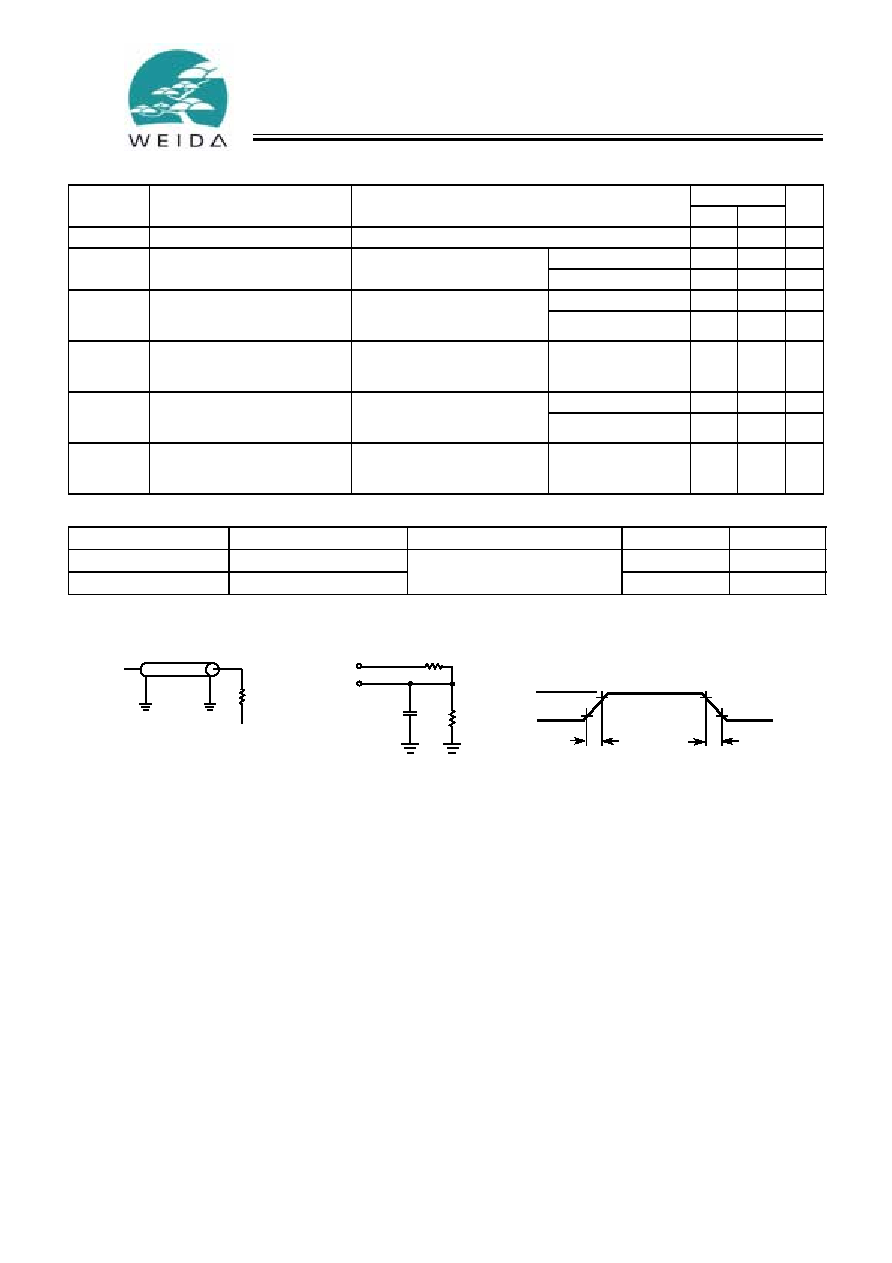
AC Test Loads and Waveforms
Notes:
7.
Not more than one output should be shorted at one time. Duration of the short circuit should not exceed 30 seconds.
8.
Tested initially and after any design or process changes that may affect these parameters.
9.
R1=1667
and R2=1538
for I
OH
/I
OL
=≠4/8 mA, R1=521
and R2=481
for I
OH
/I
OL
=≠2/2 mA.
2.5V
GND
90%
10%
90%
10%
Fall Time: 1 V/ns
OUTPUT
R1
R2
5 pF
INCLUDING
JIGAND
SCOPE
(a)
(b)
ALL INPUT PULSES
OUTPUT
R
L
=50
Z
0
=50
V
L
=1.5V
2.5V
[9]
Rise Time: 1 V/ns
WCSS0418V1F
Document #: 38-05245 Rev. **
Page 9 of 18
Switching Characteristics
Over the Operating Range
[10]
Parameter
Description
-117
-100
Min.
Max.
Min.
Max.
Unit
t
CYC
Clock Cycle Time
8.5
10
ns
t
CH
Clock HIGH
3.0
4.0
ns
t
CL
Clock LOW
3.0
4.0
ns
t
AS
Address Set-Up Before CLK Rise
2.0
2.0
ns
t
AH
Address Hold After CLK Rise
0.5
0.5
ns
t
CDV
Data Output Valid After CLK Rise
7.5
8.0
ns
t
DOH
Data Output Hold After CLK Rise
2.0
2.0
ns
t
ADS
ADSP, ADSC Set-Up Before CLK Rise
2.0
2.0
ns
t
ADH
ADSP, ADSC Hold After CLK Rise
0.5
0.5
ns
t
WES
BWS
[1:0]
, GW, BWE Set-Up Before CLK Rise
2.0
2.0
ns
t
WEH
BWS
[1:0]
, GW, BWE Hold After CLK Rise
0.5
0.5
ns
t
ADVS
ADV Set-Up Before CLK Rise
2.0
2.0
ns
t
ADVH
ADV Hold After CLK Rise
0.5
0.5
ns
t
DS
Data Input Set-Up Before CLK Rise
2.0
2.0
ns
t
DH
Data Input Hold After CLK Rise
0.5
0.5
ns
t
CES
Chip Enable Set-Up
2.0
2.0
ns
t
CEH
Chip Enable Hold After CLK Rise
0.5
0.5
ns
t
CHZ
Clock to High-Z
[11, 12]
3.5
3.5
ns
t
CLZ
Clock to Low-Z
[11, 12]
0
0
ns
t
EOHZ
OE HIGH to Output High-Z
[11, 13]
3.5
3.5
ns
t
EOLZ
OE LOW to Output Low-Z
[11, 13]
0
0
ns
t
EOV
OE LOW to Output Valid
3.5
3.5
ns
Notes:
10. Unless otherwise noted, test conditions assume signal transition time of 2.5 ns or less, timing reference levels of 1.25V, input pulse levels of 0 to 2.5V, and
output loading of the specified I
OL
/I
OH
and load capacitance. Shown in (a) and (b) of AC Test Loads.
11. t
CHZ
, t
CLZ
, t
EOHZ
, and t
EOLZ
are specified with a load capacitance of 5 pF as in part (b) of AC Test Loads. Transition is measured
±
200 mV from steady-state
voltage.
12. At any given voltage and temperature, t
CHZ
(max.) is less than t
CLZ
(min.).
13. This parameter is sampled and not 100% tested.
WCSS0418V1F
Document #: 38-05245 Rev. **
Page 10 of 18
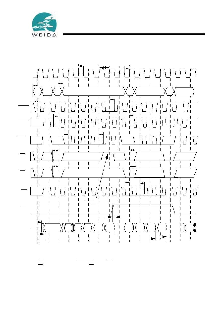
Timing Diagrams
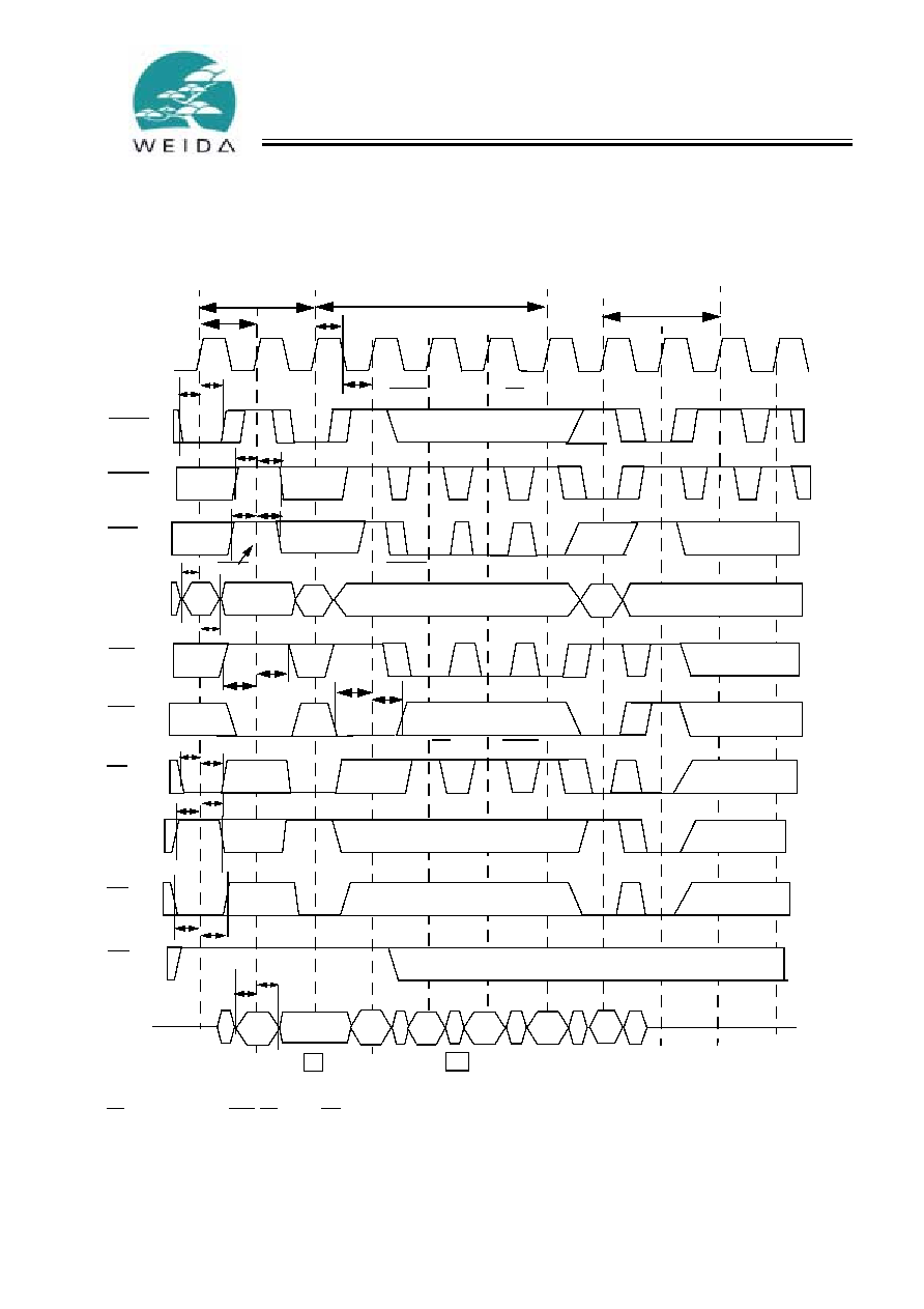
Write Cycle Timing
[14, 15]
Notes:
14. WE is the combination of BWE, BW
[3:0]
, and GW to define a write cycle (see Write Cycle Descriptions table).
15. WDx stands for Write Data to Address X.
ADSP
CLK
ADSC
ADV
ADD
CE
1
OE
GW
WE
CE
2
CE
3
1a
Data In
t
CYC
t
CH
t
CL
t
ADS
t
ADH
t
ADS
t
ADH
t
ADVS
t
ADVH
WD1
WD2
WD3
t
AH
t
AS
t
WS
t
WH
t
WH
t
WS
t
CES
t
CEH
t
CES
t
CEH
t
CES
t
CEH
2b
3a
1a
Single Write
Burst Write
Unselected
ADSP ignored with CE
1
inactive
CE
1
masks ADSP
= DON'T CARE
= UNDEFINED
Pipelined Write
2a
2c
2d
t
DH
t
DS
High-Z
High-Z
Unselected with CE
2
ADV Must Be Inactive for ADSP Write
ADSC initiated write
WCSS0418V1F
Document #: 38-05245 Rev. **
Page 11 of 18
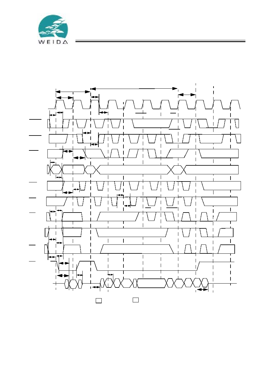
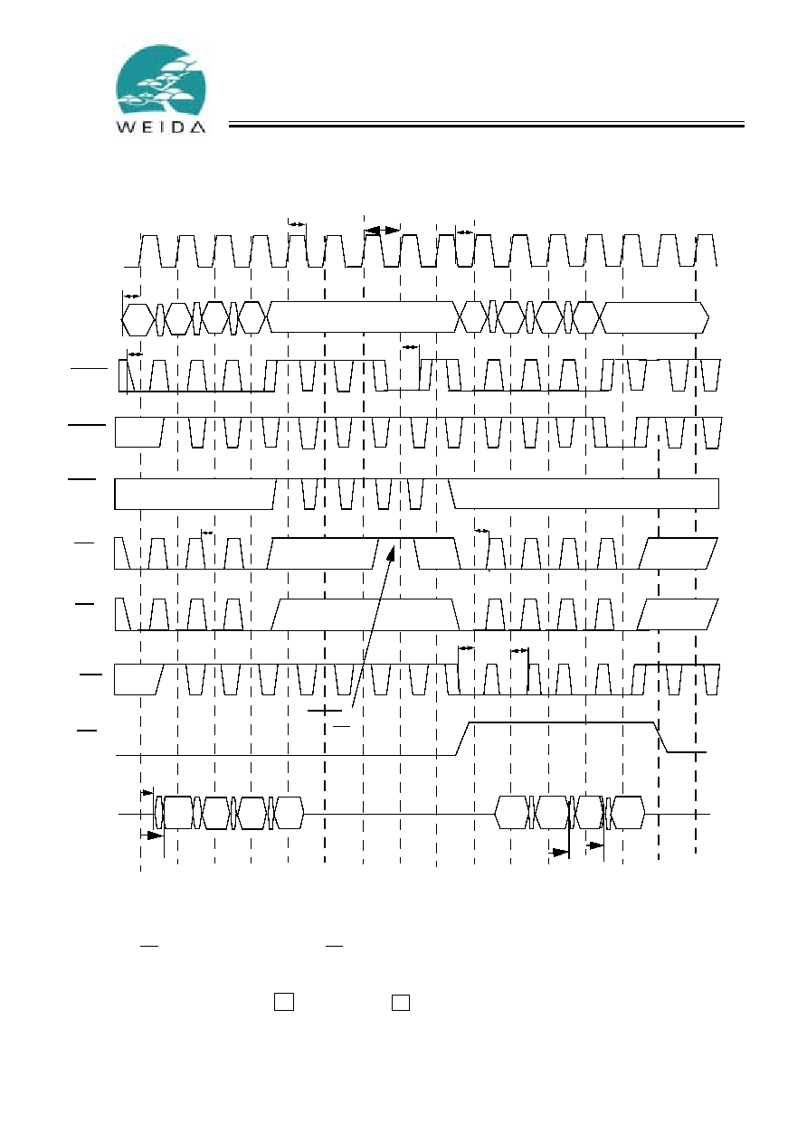
Read Cycle Timing
[14, 16]
Note:
16. RDx stands for Read Data from Address X.
Timing Diagrams
(continued)
ADSP
CLK
ADSC
ADV
ADD
CE
1
OE
GW
WE
CE
2
CE
3
2a
2c
1a
Data Out
t
CYC
t
CH
t
CL
t
ADS
t
ADH
t
ADS
t
ADH
t
ADVS
t
ADVH
RD1
RD2
RD3
t
AH
t
AS
t
WS
t
WH
t
WH
t
WS
t
CES
t
CEH
t
CES
t
CEH
t
CES
t
CEH
t
CDV
t
EOV
2b
2c
2d
3a
1a
t
OEHZ
t
DOH
t
CLZ
t
CHZ
Single Read
Burst Read
Unselected
ADSP ignored with CE
1
inactive
Suspend Burst
CE
1
masks ADSP
= DON'T CARE
= UNDEFINED
Pipelined Read
ADSC initiated read
Unselected with CE
2
WCSS0418V1F
Document #: 38-05245 Rev. **
Page 12 of 18
Read/Write Cycle Timing
Timing Diagrams
(continued)
A
t
AH
t
AS
WE is the combination of BWE, BWS
[1:0]
, and GW to define a write cycle (see Write Cycle Descriptions table)
t
CLZ
t
CHZ
CE is the combination of CE
2
and CE
3
. All chip selects need to be active in order to select
the device. RAx stands for Read Address X, WAx stands for Write Address X, Dx stands for Data-in X,
t
DOH
CLK
ADD
WE
CE
1
Data
B
C
D
ADSP
ADSC
ADV
CE
OE
Q(A)
Q(B)
Q
(B+1)
Q
(B+2)
Q
(B+3)
Q(B)
D(C)
D
(C+1)
D
(C+2)
D
(C+3)
Q(D)
t
CYC
t
CH
t
CL
t
ADS
t
ADH
t
ADS
t
ADH
t
ADVH
t
ADVS
t
CEH
t
CEH
t
CES
t
CES
t
WEH
t
WES
t
CDV
Device originally
deselected
ADSP ignored
with CE
1
HIGH
t
EOHZ
Qx stands for Data-out X.
In/Out
WCSS0418V1F
Document #: 38-05245 Rev. **
Page 13 of 18
Pipeline Timing
Timing Diagrams
(continued)
A
t
AS
= DON'T CARE
= UNDEFINED
t
CLZ
t
CHZ
CE is the combination of CE
2
and CE
3
. All chip selects need to be active in order to select
the device. RAx stands for Read Address X, WAx stands for Write Address X, Dx stands for Data-in X,
t
DOH
CLK
ADD
WE
CE
1
Data
B
ADSP
ADSC
ADV
CE
OE
Q(A)
Q(B)
Q(D)
D(C)
D (E)
D (F)
D (G)
t
CYC
t
CH
t
CL
t
ADS
t
ADH
t
CEH
t
CES
t
WEH
t
WES
t
CDV
Device originally
deselected
ADSP ignored
with CE
1
HIGH
Qx stands for Data-out X.
C
D
Q(C)
E
F
G
H
D (H)
WCSS0418V1F
Document #: 38-05245 Rev. **
Page 14 of 18
Timing Diagrams
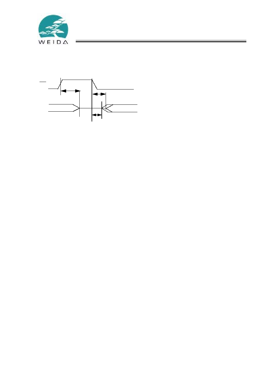
(continued)
OE
three-state
I/Os
t
EOHZ
t
EOV
t
EOLZ
OE Switching Waveforms
WCSS0418V1F
Document #: 38-05245 Rev. **
Page 15 of 18
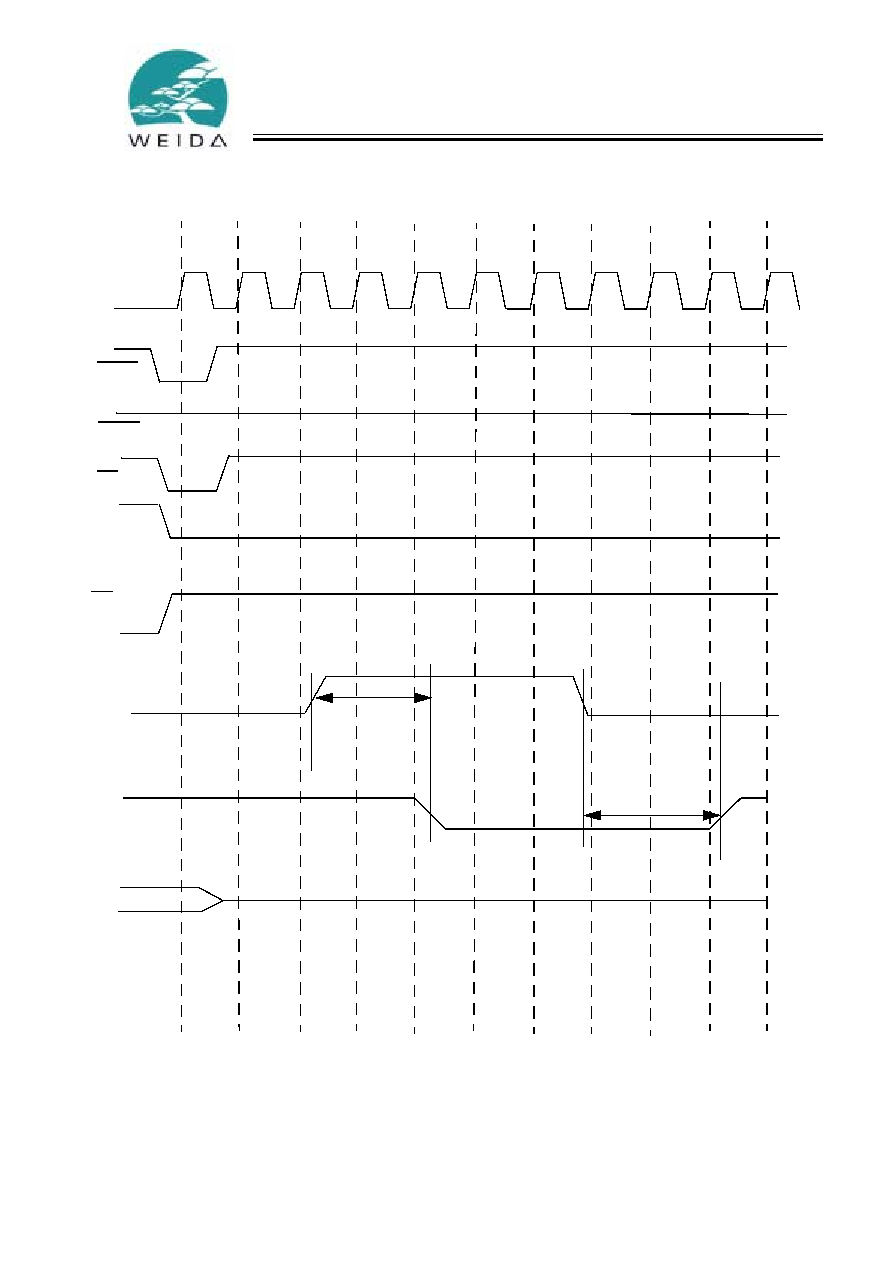
Notes:
17. Device must be deselected when entering ZZ mode. See Cycle Description Table for all possible signal conditions to deselect the device.
18. I/Os are in three-state when exiting ZZ sleep mode.
Timing Diagrams
(continued)
ADSP
CLK
ADSC
CE
1
CE
3
LOW
HIGH
ZZ
t
ZZS
t
ZZREC
I
CC
I
CC
(active)
Three-state
I/Os
ZZ Mode Timing
[17, 18]
CE
2
I
CCZZ
HIGH
WCSS0418V1F
Document #: 38-05245 Rev. **
Page 16 of 18
Ordering Information
Speed
(MHz)
Ordering Code
Package
Name
Package Type
Operating
Range
117
WCSS0418V1F-117
A101
100-Lead Thin Quad Flat Pack
Commercial
100
WCSS0418V1F-100AC
A101
100-Lead Thin Quad Flat Pack
WCSS0418V1F-100BGC
BG119
119-Ball BGA
WCSS0418V1F-100AI
A101
100-Lead Thin Quad Flat Pack
Industrial
WCSS0418V1F-100BGI
BG119
119-Ball BGA
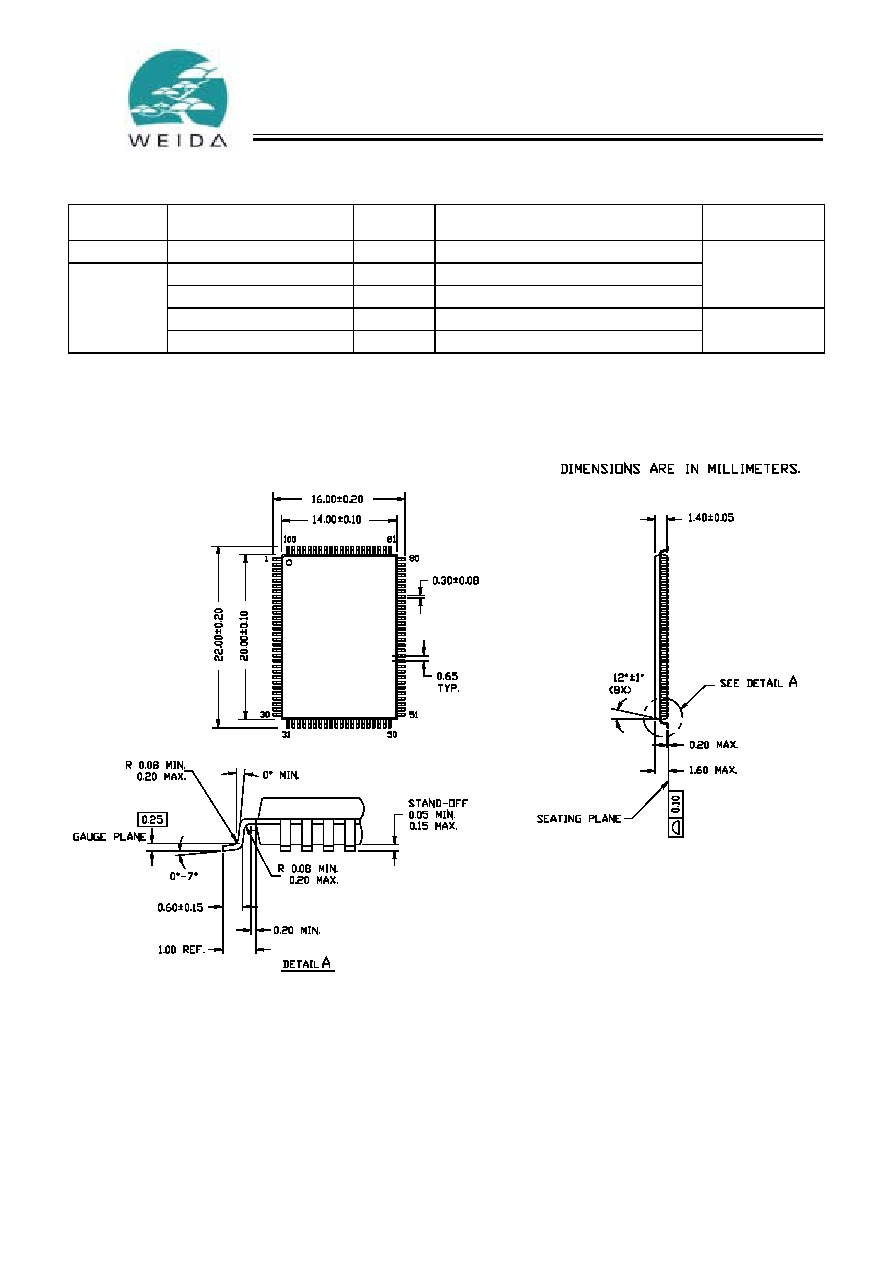
Package Diagrams
100-Pin Thin Plastic Quad Flatpack (14 x 20 x 1.4 mm) A101
51-85050-A

WCSS0418V1F
Document #: 38-05245 Rev. **
Page 17 of 18
Package Diagrams
(continued)
119-Lead FBGA (14 x 22 x 2.4 mm) BG119
51-85115

WCSS0418V1F
Document #: 38-05245 Rev. **
Page 18 of 18
Document Title: WCSS0418V1F 25Document #: 38-05245 Rev. **6K x 18 Synchronous 3.3V Cache RAM
Document Number: 38-05245
REV.
ECN NO.
Issue
Date
Orig. of
Change
Description of Change
**
109890
09/22/01
SZV
Change from Spec number: 38-05146 to 38-05245