 | –≠–ª–µ–∫—Ç—Ä–æ–Ω–Ω—ã–π –∫–æ–º–ø–æ–Ω–µ–Ω—Ç: 2N7002 | –°–∫–∞—á–∞—Ç—å:  PDF PDF  ZIP ZIP |
WEITRON
http://www.weitron.com.tw
2N7002
Rating
Symbol
Value
Unit
V
DS
V
GS
I
D
I
DM
P
D
R
JA
60
±20
250
1300
350
357
Operating Junction and Storage
Temperature Range
T
J
, Tstg
-55 to 150
C
V
V
mA
mA
mW
C/W
Drain-Source Voltage
Gate-Source Voltage
Continuous Drain Current (TA=25 C)
Pulsed Drain Current
(1)
Power Dissipation (TA=25 C)
Maximax Junction-to-Ambient
Maximum Ratings
(TA=25 C Unless Otherwise Specified)
Device Marking
2N7002=7002
Note 1:
Pulse Width Limited by Maximum Junction Temperature
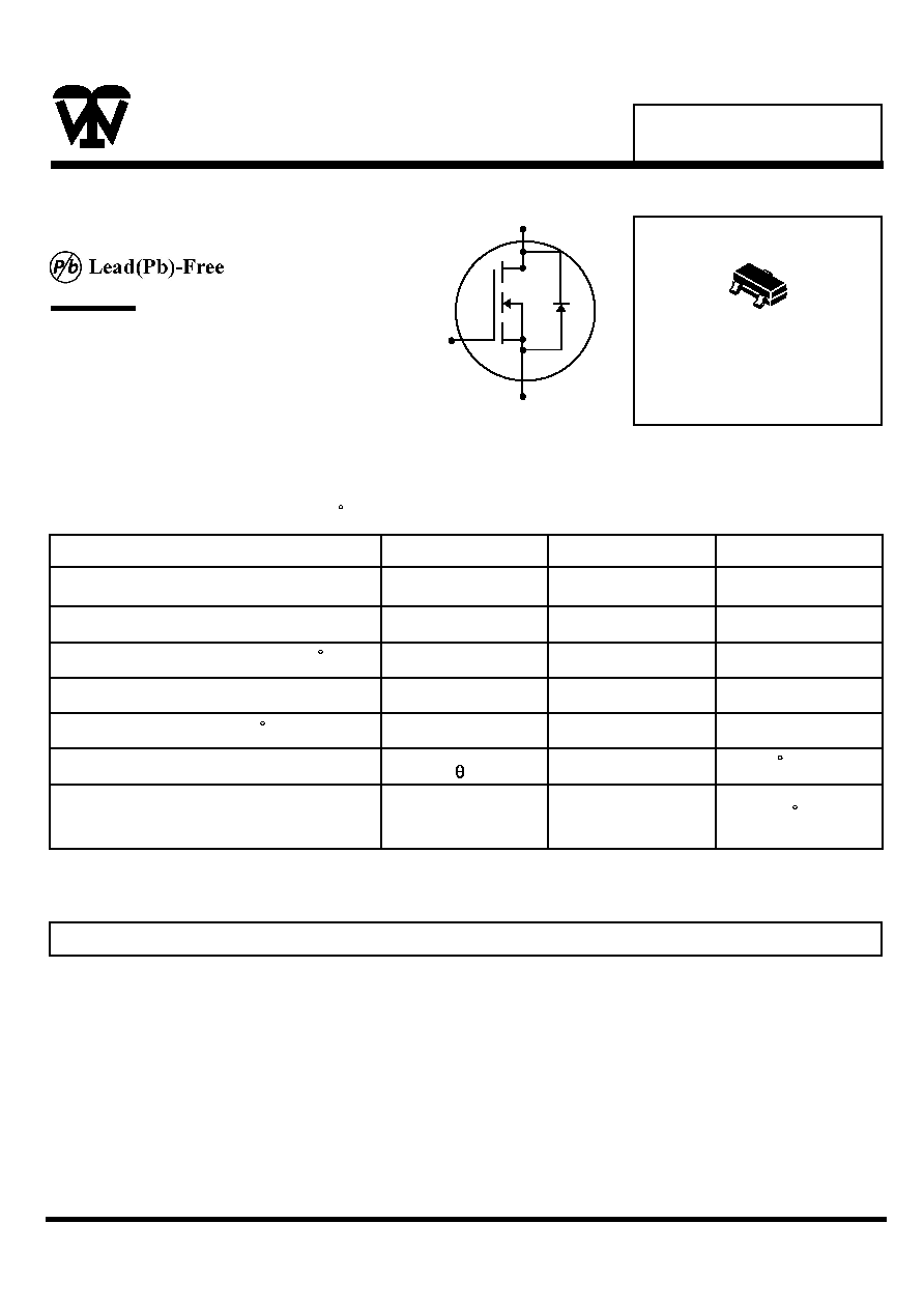
Small Signal MOSFET
N-Channel
1
2
3
GATE
SOURCE
DRAIN
SOT-23
1
2
3
Features:
*Low On-Resistance : 3
*Low Input Capacitance: 25PF
*Low Out put Capacitance : 6PF
*Low Threshole :1 .5V(TYE)
*Fast Switching Speed : 7.5ns
WEITRON
WEITRON
http://www.weitron.com.tw
2N7002
Note: 1. For Design Aid Only not Subject to Production Testing.
2. Pulse Test : PW 300µs, Duty Cycle 2%
3. Switching Time is Essentially Independent of Operating Temperature .
Total Gate Charge
V
DS
=30V, V
GS
=10V, I
D
=250mA
Gate-Source Charge
V
DS
=30V, V
GS
=10V, I
D
=250mA
Gate-Drain Charge
V
DS
=30V, V
GS
=10V, I
D
=250mA
Input Capacitance
V
DS
=25V, V
GS
=0V, f=1MHZ
Output Capacitance
V
DS
=25V, V
GS
=0V, f=1MHZ
Reverse Transfer Capacitance
V
DS
=25V, V
GS
=0V, f=1MHZ
Drain-Source Breakdown Voltage
V
GS
=0V, I
D
=10 uA
Gate-Threshold Voltage
V
DS
=V , I
D
=250 uA
Gate-body Leakage
V
DS
=0V, V
GS
=15V
On-State Drain Current
(2)
V
GS
=10V, V
DS
=7.5V
V
GS
=4.5V, V
DS
=10V
Drain-Source On-Resistance
(2)
V
GS
=10V, I
D
=250mA
V
GS
=4.5V, I
D
=200mA
Forward Transconductance
(2)
V
DS
=15V, I
D
=200mA
Diode Forward Voltage
I
S
=200mA, V
GS
=0V
Static
Dynamic
(1)
Switching
(1) (3)
Characteristic
Symbol
Unit
Min
Typ
Max
V
(BR)DSS
V
GS (th)
I
D (
on
)
r
DS (
on
)
I
GSS
I
DSS
g
fs
V
SD
g
gs
gd
C
iss
C
oss
C
rss
t
d
(
on
)
t
r
t
f
t
d(off)
60
70
V
1
1.5
2.5
V
V
-
-
-
1
500
-
-
100
nA
uA
mA
mS
800
500
1300
700
1.5
2.0
3
4
300
0.85
1.2
0.6
0.06
0.06
25
6
1.2
1.0
nC
PF
7.5
6.0
7.5
3.0
nS
nS
20
20
Electrical Characteristics
(TA=25 C Unless otherwise noted)
Zero Gate Voltage Drain Current
V
DS
=60V, V
GS
=0V
V
DS
=60V, V
GS
=0V, T
j
=125 C
-
-
-
-
-
-
-
-
-
-
-
-
-
-
-
-
-
-
-
-
-
-
-
Turn-On Time
V
DD
=30V, R
L
=200 ,I
D
=100mA
V
GEN
=10V, R
G
=10
Turn-Off Time
V
DD
=30V, R
L
=200 , I
D
=100mA
V
GEN
=10V, R
G
=10
Q
Q
Q
GS
<_
<_
WEITRON
http://www.weitron.com.tw
2N7002
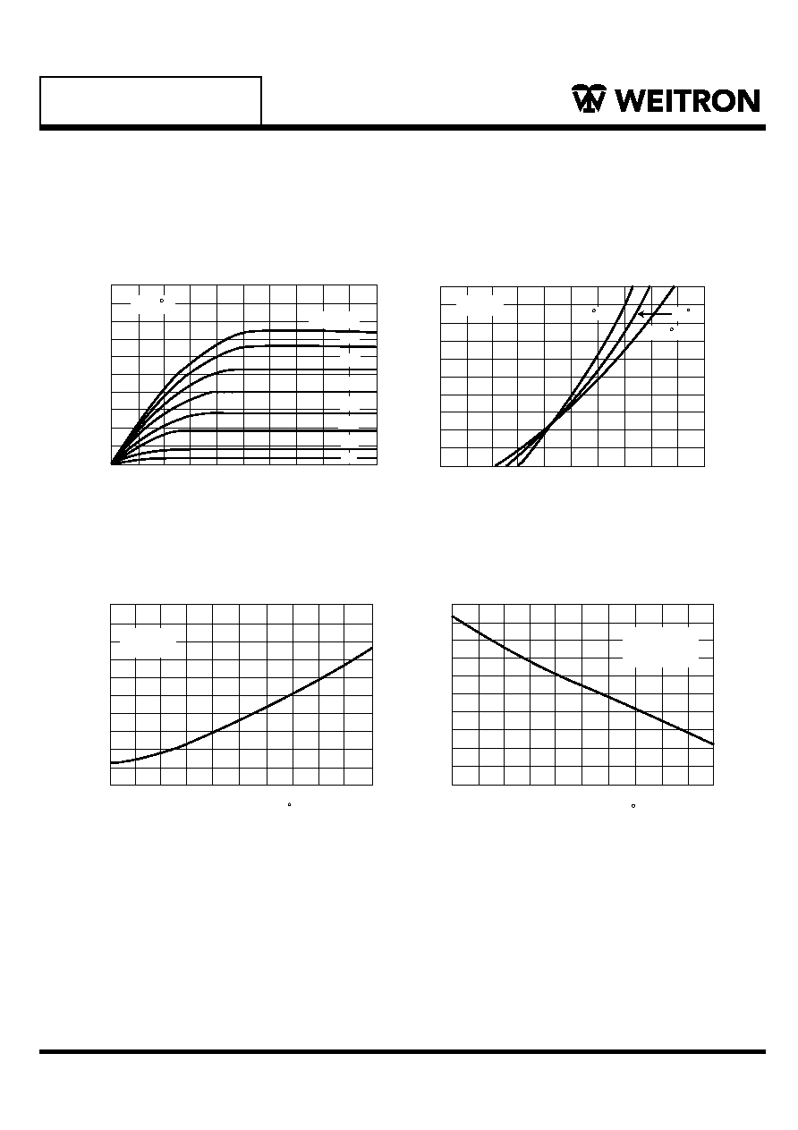
VGS, GATE SOURCE VOLTAGE (VOLTS)
FIG.2 Transfer Characteristics
0
1.0
2.0
3.0
4.0
5.0
6.0
7.0
8.0
9.0
10
1.0
0.8
0.6
0.4
0.2
0
I D
,
D
R
A
I
N
C
U
R
R
E
N
T
(
A
M
P
S
)
VDS=10V
-55 C
125 C
25 C
FIG.1 Ohmic Region
VDS, DRAIN SOURSE VOLTAGE (VOLTS)
2.0
1.8
1.6
1.4
1.2
1.0
0.8
0.6
0.4
0.2
0
TA=25 C
VGS=10V
9V
8V
7V
6V
5V
4V
3V
0
1.0
2.0
3.0
4.0
5.0
6.0
7.0
8.0
9.0
10
I D
,
D
R
A
I
N
C
U
R
R
E
N
T
(
A
M
P
S
)
FIG.4 Temperature Versus Gate
Threshold Voltage
-60
-20
+20
+80
+100
+140
1.2
1.05
1.1
1.10
1.0
0.95
0.9
0.85
0.8
0.8
0.75
0.7
V G
S (
t
h
)
,
T
H
R
E
S
H
O
L
D
V
O
L
T
A
G
E
(
N
O
R
M
A
L
I
Z
E
D
)
VDS = VGS
ID = 1.0mA
T,TEMPERATURE ( C)
FIG.3 Temperature Versus Static
Drain-Sourse On-Resistance
T,TEMPERATURE ( C)
2.4
2.2
2.0
1.8
1.6
1.4
1.2
1.0
0.8
0.6
0.4
r
D
S
(
O
N
)
,
S
T
A
T
I
C
D
R
A
I
N
-
S
O
U
R
S
E
O
N
-
R
E
S
I
S
T
A
N
C
E
(
N
O
R
M
A
L
I
Z
E
D
)
VGS = 10V
ID=200mA
-60
-20
+20
+80
+100
+140
WEITRON
http://www.weitron.com.tw
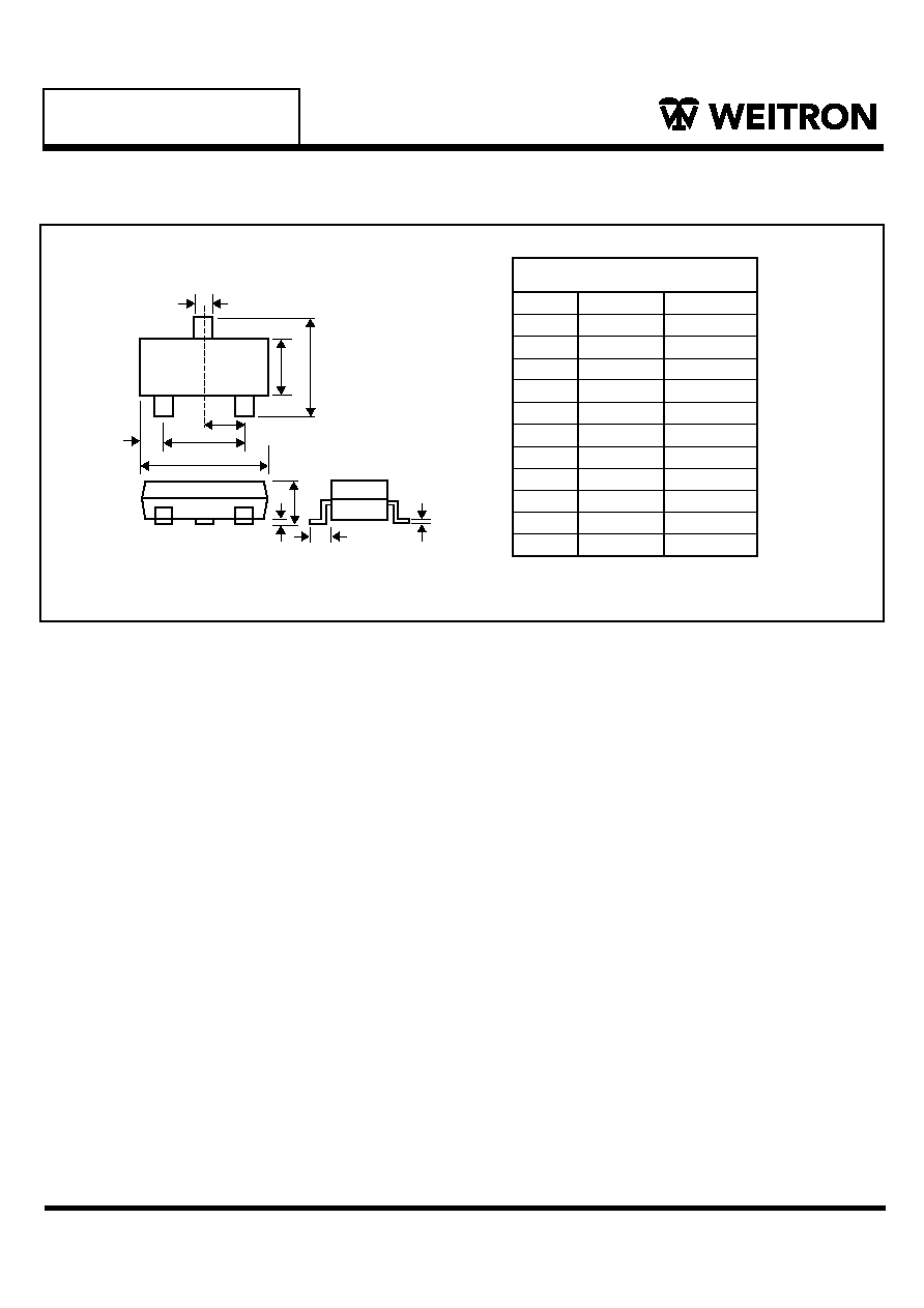
Dim
A
B
C
D
E
G
H
J
K
L
M
Min
0.35
1.19
2.10
0.85
0.46
1.70
2.70
0.01
0.89
0.30
0.076
Max
0.51
1.40
3.00
1.05
1.00
2.10
3.10
0.13
1.10
0.61
0.25
A
B
D
E
G
M
L
H
J
TOP VIEW
K
C
SOT-23
SOT-23 Outline Dimension
2N7002