 | –≠–ª–µ–∫—Ç—Ä–æ–Ω–Ω—ã–π –∫–æ–º–ø–æ–Ω–µ–Ω—Ç: BAS19H | –°–∫–∞—á–∞—Ç—å:  PDF PDF  ZIP ZIP |
Surface Mount Switching Diode
Features:
BAS19H/BAS20H
WEITRON
SWITCHING DIODE
200mAMPERS
120-250VOLTS
http://www.weitron.com.tw
BAS21H
*Fast Switching Speed
*Surface Mount Package Ideally
*High Conductance
*For General Purpose Switching Applications
Mechanical Data:
*Case: SOD-323 Molded Plastic
*Terminals: Solderable Per MIL-STD-202, Method 208
*Polarity: See Eqivalent Circuit Diagram
*Weight: 0.004grams(approx)
Suited for
Automatic Insertion
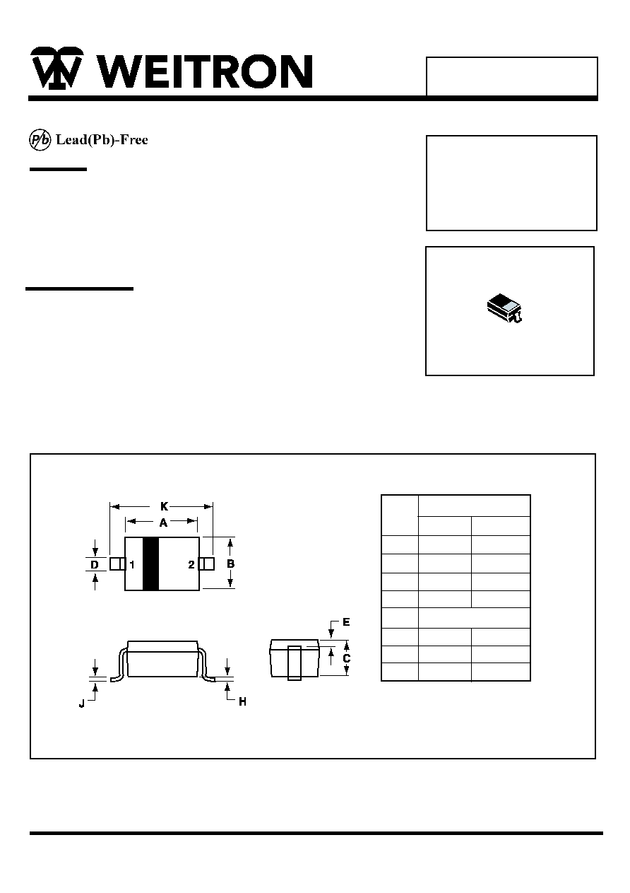
SOD-323
1
2
Unit:mm
Dim Min Max
A
B
C
D
E
H
J
K
1.60 1.80
1.15 1.35
0.80 1.00
0.25 0.40
0.15 REF
0.00 0.10
0.089 0.377
2.30 2.70
PIN 1.CATHODE
2.ANODE
MILLMETERS
SOD-323 Outline Demensions

WEITRON
WE IT R ON
Maximum Ratings
(TA=25 C Unless otherwise noted)
Electrical Characteristics
(TA=25 C Unless otherwise noted)
Characteristic
Symbol
Forward Voltage
Total Capacitance
(VR=1.0V, f=1.0MHz)
Reverse Leakage
@Rated DC Blocking Voltage
IR
Cj
VF
Max
Unit
Volts
PF
nAdc
http://www.weitron.com.tw
BAS19H/BAS20H
BAS21H
IF
IF
=100mA
=200mA
1.0
1.25
-
-
-
5.0
100
50
Min
Reverse Recovery Time
IF R
= I =30mA
I rr =0.1*IR ,RL=100
W
trr
nS
NOTE:
1. Valid provided that terminals are kept at ambient temperature.
BAS19H
BAS20H
BAS21H
Non-Repetitive
Non-Repetitive
Peak Reverse Voltage
Working Peak Reverse Voltage
DC Blocking Voltage
Forward Continuous Current
(1)
(1)
(1)
Average Rectified Output Current
Peak Forward Surge Current
@t=1.0us
@t=1.0s
Power Dissipation
Thermal Resistance Junction to
Ambient Air
Operating and Storage
Temperature Range
V
RRM
V
R
V
RWM
V
R(RMS)
IFM
Io
I FSM
Pd
R JA
T j ,T
STG
120
100
71
106
140
V
200
150
250
200
400
200
2.5
0.5
200
625
-65 to +150
Volts
Volts
mA
mA
A
mW
C/W
C
Characteristic
Symbol
Unit
RMS Reverse Voltage

WEITRON
http://www.weitron.com.tw
BAS19H/BAS20H
10
1.0
100
1000
0.1
0.01
0
1
2
I
,
I
N
S
T
A
N
T
A
N
E
O
U
S
F
O
R
W
A
R
D
C
U
R
R
E
N
T
(
m
A
)
F
V , INST ANT ANEOUS FOR WARD VOL TAGE (V)
Fi g. 1 Forward Characteristics
F
T = 25 C
j
∞
1
10
100
0.1
0.01
0
100
200
I
,
L
E
A
K
A
G
E
C
U
R
R
E
N
T
(
A
)
R
T , JUNCTION TEMPERA TURE ( C )
Fig. 2 Leakage Current vs Junction Temperature
j
∞
u
Device Marking
Item
Marking
Eqivalent Circuit diagram
2
1
BAS19
BAS20
BAS21
JP , A8
JR , T2
JS , T3
BAS21H