Surface Mount Switching Multi-Chip
Diode Array
Mechanical Data:
* Case : SOT-363
* Fast Switching Speed
* Ultra-Small Surface Mount Package
* For General Purpose Switching Applications
* High Conductance Power Dissipation
* Case Material : Molded Plastic. UL Flammability
Classification Ration 94V-0
* Moisture Sensitivity : Level 1 per J-STD-020C
* Terminals : Solderable per MIL-STD-202, Method 208
* Polarity : See Diagram
* Weight : 0.006 grams(appro)
Features:
WEITRON
BAS16TDW
MMBD4148TDW
MULTI-CHIP DIODES
150m AMPERES
75 VOLTS
http://www.weitron.com.tw
SOT-363
1 2
3
6 5
4
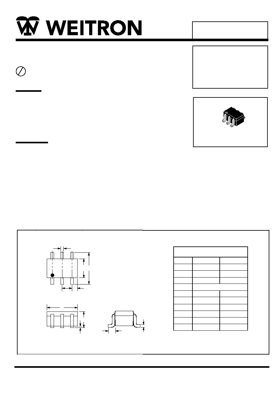
SOT-363 Outline Dimensions
Unit:mm
1
2
3
A
K
J
M
L
6
5
4
B
D
H
E
C
Dim
A
B
C
D
E
H
J
K
L
M
Min
0.10
1.15
2.00
0.30
1.80
-
0.80
0.25
0.10
0.65 REF
Max
0.30
1.35
2.20
0.40
2.20
0.10
1.10
0.40
0.25
SOT-363
1/3
09-Feb-06
Lead(Pb)-Free
P b

WEITRON
http://www.weitron.com.tw
2/3
09-Feb-06
Characteristic
Symbol
Value
Unit
100
V
Peak Repetitive Reverse Voltage
Working Peak Reverse Voltage
DC Blocking Voltage
V
RRM
V
RWM
V
R
75
V
RMS Reverse Voltage
V
R(RMS)
53
V
Forward Continuous Current (Note 1)
I
FM
300
mA
Average Rectified Output Current (Note 1)
I
O
150
mA
Non-Repetitive Peak Forward Surge Current@ t = 1.0µs
@ t = 1.0s
I
FSM
2.0
1.0
A
Power Dissipation (Note 1)
P
D
200
mW
Thermal Resistant Junction to Ambient Air (Note 1)
R
JA
625
∞C/W
Operating Temperature Range
Storage Temperature Range
T
j
T
STG
+150
-55 to +150
∞C
∞C
@ T
A
= 25∞C unless otherwise specified
Characteristic
Symbol
Min
Max
Unit
Reverse Breakdown Voltage (Note 2)
I
R
= 100µA
75
-
V
Forward Voltage (Note 2)
I
F
= 1.0mA
I
F
= 10mA
I
F
= 50mA
I
F
= 150mA
-
-
-
-
0.715
0.855
1.0
1.25
V
-
1.0
50
30
25
µA
µA
µA
nA
Total Capacitance
V
R
= 0V, f = 1.0MHz
-
2.0
pF
-
4.0
ns
Maximum Ratings
@ T
A
= 25∞C unless otherwise specified
Electrical Characteristics
Non-Repetitive Peak Reverse Voltage
Notes:1. Device mounted on FR-4 PCB, 1 inch x 0.85 inch x 0.062 inch
V
RM
Notes:2. Short duration test pulse used to minimize self-heating effect.
Reverse Current (Note 2)
V
R
= 75V
V
R
= 75V, Tj = 150∞C
V
R
= 25V, Tj = 150∞C
V
R
= 20V
Reverse Recovery Time
I
F
= I
R
=10mA, Irr=0.1 x I
R
, R
L
=100
V
(BR)R
V
F
I
R
C
T
Trr
BAS16TDW
MMBD4148TDW

WEITRON
http://www.weitron.com.tw
3/3
09-Feb-06
Typical Characteristics
Fig.1 Typical Forward Characteristics
V
F
,INSTANTANEOUS FORWARD VOLTAGE (V)
I
F
,INSTANTANEOUS FORWARD CURRENT (mA)
Fig.2 Typical Reverse Characteristics
I
R
,INSTANTANEOUS REVERSE CURRENT (nA)
V
R
, REVERSE VOLTAGE(V)
Fig.3 Typical Capacitancevs .Reverse Voltage
V
R
,REVERSEVOLTAGE(V)
C
T
,TOTAL CAPACITANCE (pF)
Fig.4 Power Derating Curve, Total Package
P
d
,POWER DISSIPATION (mW)
T
A
, AMBIENT TEMPERATURE (∞C)
0.1
1
0.01
0.001
0
1.5
1.0
0.5
T = -40∫C
A
T = 150∫C
A
T = 75∫C
A
T = 25∫C
A
T = 0∫C
A
0.1
1
10
100
1000
10000
0
20
40
60
80
100
T = -40∫C
A
T = 25∫C
A
T = 75∫C
A
T = 125∫C
A
T = 150∫C
A
T = 0∫C
A
0
50
100
150
200
250
25
0
50
75
100
125
150
300
0.0
0.2
0.4
0.6
0.8
1.8
1.6
1.4
1.2
1.0
2.0
0
10
20
40
30
f = 1.0MHz
KA2
BAS16TDW
MMBD4148TDW
Device Marking
Item
Marking
Eqivalent Circuit diagram
6
1
5
2
4
3
BAS16TDW
MMBD4148TDW