*For Surface Mount Application
*Glass Passivated Chip
*Low Reverse Leakage Current
*Low Forward Voltage Drop And High Current Capability
*Plastic Meterial Has UL Flammability Classification 94V-0
REVERSE VOLTAGE
50 TO 1000 VOLTS
FORWARD CURRENT
0.5 AMPERE
http://www.weitron.com.tw
US05AM thru
Surface Mount Ultra Fast Recovery
Features:
WEITRON
Rectifiers
US05MM
Mechanical Data:
* Polarity: Indicated by Cathode Band
* Case: Molded Plastic, MINI-SMA(Similar to SOD-123F)
* Terminals: Solder Plated, Solderable per ML-STD-750 Medthod 2026
* Wight: 0.040 grams
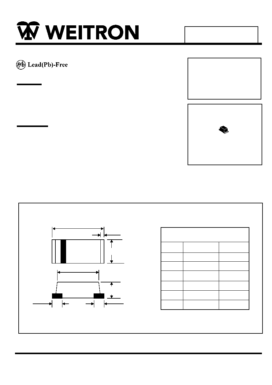
MINI-SMA Outline Dimension
unit:mm
A
C
B
E
H
J
H
3.70
4.10
1.40
1.80
-
0.30
(TYP)
E
2.80
3.20
H
-
0.90
(TYP)
J
1.40
1.60
A
B
C
MINI-SMA
Dim
Min
Max
MINI-SMA
(SOD-123F)
Maximum Ratings and Electrical Characteristics
Characteristics
Symbol
Unit
Maximum Recurrent Peak Reverse Voltage
Maximum RMS Voltage
Maximum DC Blocking Voltage
Maximum Average Forward
Rectified Current @T =50 C
Peak Forward Surge Current,
8.3 ms Single Half Sine-Wave
Superimposed on Rated Load (JEDEC Method)
Maximum Instantaneous At 0.5A DC
Maximum DC Reverse Current @T =25 C
At Rated DC Blocking Voltage @T =100 C
Maximum Reverse Recovery Time
Typical Junction Capacitance (Note 1)
Typical Thermal Resistance (Note 2)
Operating Temperature Range
Storage Temperature Range
V
V
V
A
A
V
uA
C
C
Rating 25 C Ambient Temperature Unless Otherwise Specified.
Single Phase Half Wave, 60Hz , Resistive or Inductive Load.
For Capacitive Load, Derate Current by 20%.
V
V
VDC
I
I
V
I
C
JA
T
T
50
35
50
100
70
100
200
140
200
400
280
400
600
420
600
-55 to+150
-55 to+150
F
C/W
1.Measured at 1.0MHz applied reverse voltage of 4.0V DC.
2.Thermal Resistance Junction to Ambient.
5.0
150
20(TYP)
42(TYP)
http://www.weitron.com.tw
WEITRON
J
J
US05AM thru
P
R
T
NOTES:
800
560
800
1000
700
1000
0.5
30
1.3
50
75
1.7
1.0
US05MM
US
05AM
US
05BM
US
05DM
US
05GM
US
05JM
US
05KM
US
05MM
A
A
A
Device Marking
Item
Marking
US05AM
US05BM
US05DM
US05GM
US05JM
US05KM
US05MM
U1
U2
U3
U4
Item
Marking
U5
U6
U7
RR
R
F(AV)
FSM
RRM
RMS
F
STG
ns
US05AM thru
WEITRON
http://www.weitron.com.tw
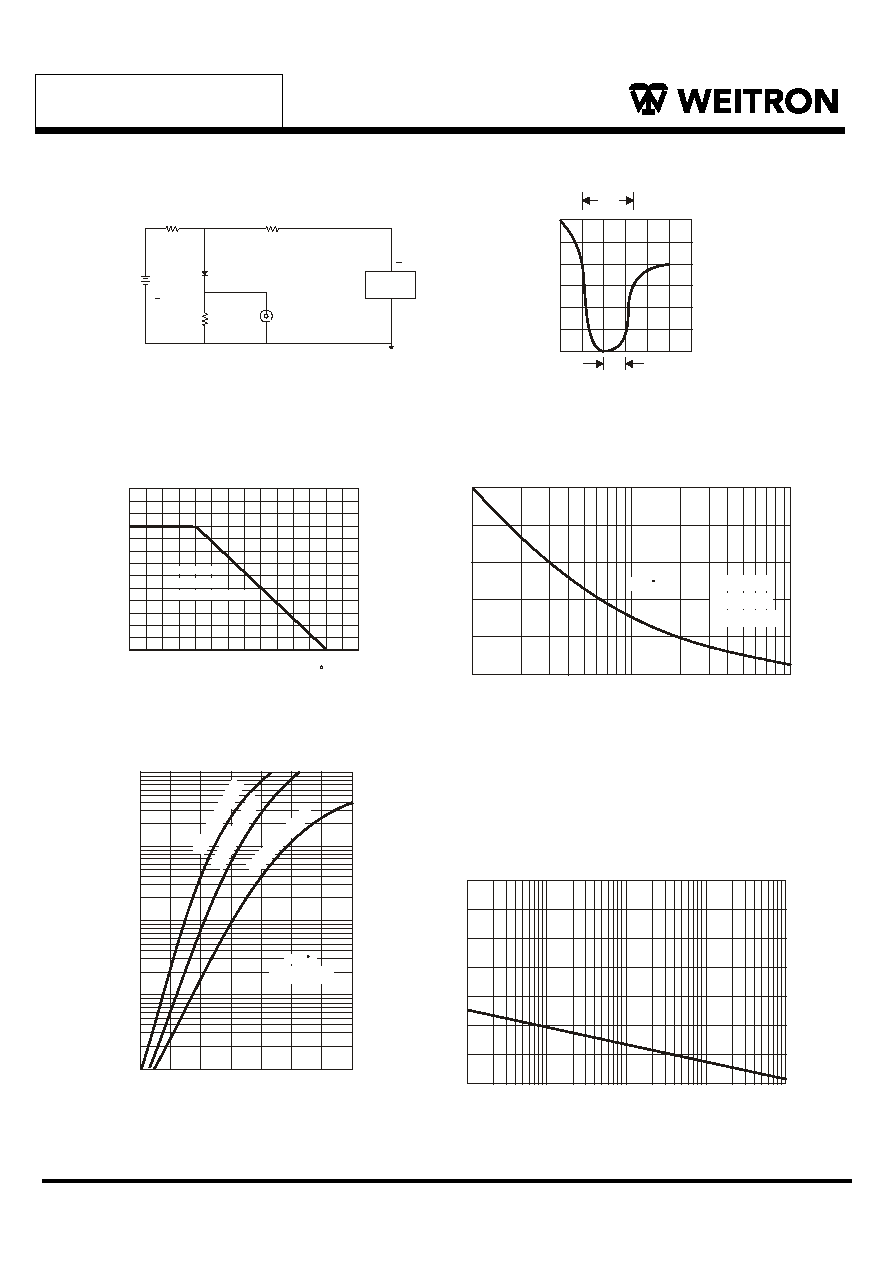
RATING AND CHARACTERISTIC CURVES
FIG.1- Test Circuit Diagram and Reverse
Recovery Time Characteristics
US05MM
FIG.4-Typical Forward
Characteristics
.4
.6
.8
1.0 1.2 1.4
.001
.01
.1
1.0
10
I
N
S
T
A
N
T
A
N
E
O
U
S
F
O
R
W
A
R
D
C
U
R
R
E
N
T
,
(
A
)
FORWARD VOLTAGE,(V)
Pulse Width 300us
1% Duty Cycle
Tj=25 C
1.6 1.8
US
05
AM
-U
S0
5D
M
US
05
G
M
-U
S0
5J
M
US
05
KM
-U
S0
5M
M
FIG.2-Tyical Forward Current Derating Curve
A
V
E
R
A
G
E
F
O
R
W
A
R
D
C
U
R
R
E
N
T
,
(
A
)
0.1
0.2
0.3
0.4
0.5
0.6
Single Phase
Half Wave 60Hz
Resistive Or Inductive Load
AMBIENT TEMPERATURE ( C)
0
25
50 75 100 125 150 175
0
(+)
(+)
25Vdc
(approx.)
( )
( )
PULSE
GENERATOR
(NOTE 2)
OSCILLISCOPE
(NOTE 1)
1
NON-
INDUCTIVE
W
NOTES: 1. Rise Time= 7ns max., Input Impedance= 1 megohm.22pF.
2. Rise Time= 10ns max., Source Impedance= 50 ohms.
+0.5A
0
-0.25A
-1.0A
|
|
|
|
|
|
|
|
1cm
SET TIME BASE FOR
50 / 10ns / cm
trr
D.U.T.
10
NONINDUCTIVE
50
NONINDUCTIVE
W
W
FIG.3-Maximum Non-repetitive Forward
Surge Current
6
0
12
18
24
30
NUMBER OF CYCLES AT 60Hz
1
10
5
50
100
Tj=25 C
8.3ms Single Half
Sine Wave
JEDEC method
P
E
A
K
F
O
R
W
A
R
D
S
U
R
G
E
C
U
R
R
E
N
T
,
(
A
)
FIG.5-Typical Junction Capacitance
REVERSE VOLTAGE,(V)
J
U
N
C
T
I
O
N
C
A
P
A
C
I
T
A
N
C
E
,
(
p
F
)
175
120
100
80
60
40
20
0
.01 .05 .1 .5 1 5 10 50 100