 | –≠–ª–µ–∫—Ç—Ä–æ–Ω–Ω—ã–π –∫–æ–º–ø–æ–Ω–µ–Ω—Ç: WTL2622 | –°–∫–∞—á–∞—Ç—å:  PDF PDF  ZIP ZIP |
Document Outline
- Switching1.doc
- WTN9973-4.pdf
- WTN9973-5.pdf
- WTN9973-6.pdf
- Switchinga.pdf

WEITRON
http:www.weitron.com.tw
DRAIN CURRENT
2.5 AMPERES
DRAIN SOURCE VOLTAGE
20 VOLTAGE
Features:
*Super High Dense Cell Design For Low R
DS(ON)
R
DS(ON)
< 80m@V
GS
=4.5V
*Rugged and Reliable
*Capable of 2.5V Gate Drive
*Simple Drive Requirement
*SOT-26 Package
Maximum Ratings
(T
A
=25∞C Unless Otherwise Specified)
Rating
Symbol
Value
Unit
Drain-Source Voltage
V
DS
20
V
Gate-Source Voltage
V
GS
±10
Continuous Drain Current
1
, V
GS
@4.5V, T
A
=25∞C
2.5
I
D
8
Drain-Source Diode Forward Current
1
I
DM
I
S
1.25
A
Total Power Dissipation
1
(T
A
=25∞C)
P
D
1
W
Maximum Junction-ambient
1
R
JA
125
∞C/W
Operating Junction and Storage Temperature Range
T
J
,T
stg
-55~+150
∞C
Device Marking
WTL2622=STS2622
WTL2622
Dual N-Channel Enhancement
Mode MOSFET
2 SOURCE
1 GATE
6 DRAIN
5 SOURCE
3 GATE
4 DRAIN
SOT-26
19-Sep-05
1/6
Lead(Pb)-Free
P b
-Pulsed
2
1
2
3
4
5
6
WTL2622
WEITRON
http:www.weitron.com.tw
2/6
19-Sep-05
Electrical Characteristics
(T
A
= 25 Unless otherwise noted)
Characteristic
Symbol Min
Typ
3
Max
Unit
OFF Characteristics
ON Characteristics
2
Drain-Source Breakdown Voltage
V
GS
=0,I
D
=250A
BV
DSS
20
-
-
0.8
1.5
Gate-Source Threshold Voltage
V
DS
=V
GS
,I
D
=250A
V
GS(Th)
0.5
V
V
Gate-Source Leakage current
V
GS
=±10V, V
DS
=0V
I
GSS
I
DSS
I
D(ON)
-
-
±100
nA
-
-
1
-
Drain-Source Leakage Current
V
DS
=16V,V
GS
=0V
On-State Drain Current
V
DS
=5V,V
GS
=4.5V
6
-
A
A
Drain-Source On-Resistance
V
GS
=4.5V,I
D
=2.5A
V
GS
=2.5V,I
D
=2.0A
R
DS(on)
-
65
80
-
90
110
m
Forward Transconductance
V
DS
=5V,I
D
=2.5A
gfs
-
7
Dynamic Characteristics
3
Input Capacitance
V
GS
=0V,V
DS
=10V,f=1.0MHz
V
GS
=0V,V
DS
=10V,f=1.0MHz
V
GS
=0V,V
DS
=10V,f=1.0MHz
C
iss
-
220
-
Output Capacitance
C
oss
-
67
-
Reverse Transfer Capacitance
C
rss
-
50
-
pF
-
S
WTL2622
Note: 1. Surface mounted on 1 in2 copper pad of FR4 board, t 10sec.
2. Pulse Test : Pulse width 300µs, duty cycle 2%.
3. Guaranteed by design, not subject to production testing.
3/6
19-Sep-05
WEITRON
http:www.weitron.com.tw
Switching Characteristics
3
Turn-on Delay Time
2
V
DS
=10V, V
GS
=4.5V, I
D
=1A, R
GEN
=6
V
DS
=10V, V
GS
=4.5V, I
D
=1A, R
GEN
=6
V
DS
=10V, V
GS
=4.5V, I
D
=1A, R
GEN
=6
V
DS
=10V, V
GS
=4.5V, I
D
=1A, R
GEN
=6
V
DS
=10V,V
GS
=4.5V,I
D
=2.5A
V
DS
=10V,V
GS
=4.5V,I
D
=2.5A
V
DS
=10V,V
GS
=4.5V,I
D
=2.5A
t
d(on)
t
d(off)
-
10.2
-
Rise Time
t
r
t
f
-
8.3
-
Turn-off Delay Time
-
13.5
-
Fall Time
-
12.7
-
ns
Total Gate Charge
2
Q
g
Q
gs
Q
gd
-
4
-
Gate-Source Charge
-
1.5
-
Gate-Source Change
-
0.7
-
nC
Source-Drain Diode Characteristics
2
Forward On Voltage
V
GS
=0V,I
S
=1.25A
V
SD
-
0.84
1.2
V
Electrical Characteristics
(T
A
= 25 Unless otherwise noted)
Characteristic
Symbol Min
Typ
3
Max
Unit
WEITRON
http://www.weitron.com.tw
WTL2622
4/6
19-Sep-05
V
DS
, Drain-to Source Voltage (V)
V
GS
, Gate-to-Source Voltage (V)
V
DS
, Drain-to-Source Voltage (V)
I
D
,
D
r
a
i
n
C
u
r
r
e
n
t
(
A
)
C,
C
apacitanc
e (pF)
I
D
,
D
r
ain C
ur
r
en
t (A)
Ciss
Coss
500
400
300
200
100
0
20
16
12
8
4
0
0
0.5
1
1.5
2
2.5
3
V
GS
=4V
V
GS
=2V
2.2
1.8
1.4
1.0
0.6
0.2
0
-50
0
50
100 125
Tj (∞C)
-25
25
75
V
GS
=4.5V
I
D
=2.5A
Crss
25 C
15
12
9
6
3
0
0.0
0.6
1.2
1.8
2.4
3.0
3.6
Tj=125 C
-55 C
V
GS
=3V
V
GS
=4.5V
V
GS
=10V
R
DS(ON)
,
On-R
esistanc
e
N
or
maliz
ed
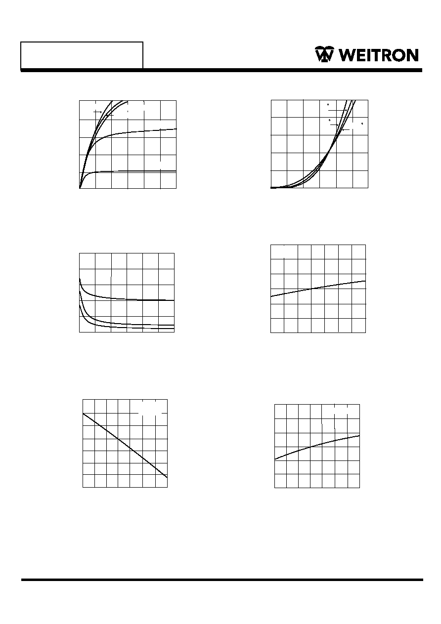
Fig.1 Output Characteristics
Fig.2 Transfer Characteristics
Fig.4 On-Resistance Variation with
Temperature
Fig.3 Capacitance with Drain to Source
Voltage
0 5 10 15 20 25 30
Fig.6 Breakdown Voltage Variation
with Temperature
Fig.5 Gate Threshold Voltage Variation
with Temperature
V
t
h
,
N
o
r
m
a
l
i
z
e
d
G
a
t
e
-
S
o
u
r
c
e
T
h
r
e
s
h
o
l
d
V
o
l
t
a
g
e
B
V
D
S
S
,
N
o
r
m
a
l
i
z
e
d
D
r
a
i
n
-
S
o
u
r
c
e
B
r
e
a
k
d
o
w
n
V
o
l
t
a
g
e
Tj, Junction Temperature (∞C)
Tj, Junction Temperature (∞C)
-50 -25
0
25 50
75 100 125
1.3
1.2
1.1
1.0
0.9
0.8
0.7
I
D
=250uA
1.3
1.2
1.1
1.0
0.9
0.8
0.7
0.6
-50 -25
0
25 50
75 100 125
V
DS
=V
GS
I
D
=250uA
WEITRON
http://www.weitron.com.tw
WTL2622
5/6
19-Sep-05
g
F
S
,
T
r
a
n
s
c
o
n
d
u
c
t
a
n
c
e
(
S
)
V
G
S
,
G
a
t
e
t
o
S
o
u
r
c
e
V
o
l
t
a
g
e
(
V
)
I
s
,
S
o
u
r
c
e
-
d
r
a
i
n
c
u
r
r
e
n
t
(
A
)
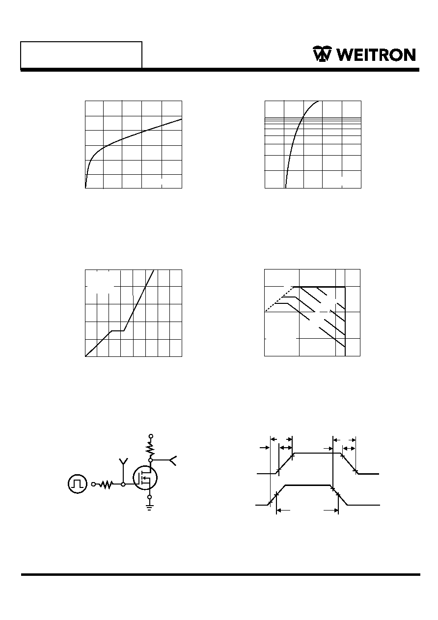
Fig.7 Transconductance Variation
with Drain Current
I
DS
, Drain-Source Current (A)
Fig.9 Gate Charge
Qg, Total Gate Charge (nC)
Fig.10 Maximum Safe Operating Area
V
DS
, Drain-Source Voltage (V)
Fig.8 Body Diode Forward Voltage
Variation with Source Current
V
SD
, Body Diode Forward Voltage (V)
I
D
,
D
r
a
i
n
C
u
r
r
e
n
t
(
A
)
20
10
0
1
0.4
0.8
1.2
1.6
2.0
2.4
4
5
3
2
1
0
0
0.7 1.4 2.1 2.8 3.5 4.2 4.9 5.6
V
DS
=4.5V
I
D
=2.5A
T
J
=25∞C
50
10
1
0.1
0.03
0.1
1
10 20
50
R
DS
(ON
) L
im
it
10m
s
100
ms
1s
DC
V
GS
=4.5V
Single Pulse
Tc=25∞C
10
8
6
4
12
0
0
3
6
9
12
15
2
V
DS
=5V
Fig.11 Switching Test Circuit
Fig.12 Switching Waveforms
t
V
V
t
t
d(on)
OUT
IN
on
r
10%
t
d(off)
90%
10%
10%
50%
50%
90%
t
off
t
f
90%
PULSE WIDTH
INVERTED
V
DD
R
D
V
V
R
S
V
G
GS
IN
GEN
OUT
L