 | –≠–ª–µ–∫—Ç—Ä–æ–Ω–Ω—ã–π –∫–æ–º–ø–æ–Ω–µ–Ω—Ç: WT274C | –°–∫–∞—á–∞—Ç—å:  PDF PDF  ZIP ZIP |

Weltrend Semiconductor, Inc.
2F, No. 24, Industry E. 9
th
RD., Science-Based Industrial Park, Hsin-Chu, Taiwan
TEL:886-3-5780241 FAX:886-3-5794278.5770419
Email:support@weltrend.com.tw
WT272C/WT274C
Dual/Quad Low Power CMOS OP Amplifiers
Data Sheet
REV. 1.1
December 31, 1999
The information in this document is subject to change without notice.
©
Weltrend Semiconductor, Inc. All Rights Reserved.
WT272C/WT274C
Data Sheet Rev. 1.1
Weltrend Semiconductor, Inc.
Page 2
DESCRIPTION
The WT272C/WT274C is a dual/quad low power CMOS operational amplifiers IC. It provides high
performance operation at low supply voltages. The basic amplifier can operate at supply voltage as low as
1.2V with very low power consumption and makes it perfect for battery-powered application. The input
common-mode voltage extends to the negative rail. The output swings to both rails with light load. The input
bias current is inherently low and the input impedance is extremely high. The devices are ideal upgrades for
industrial standards OP amp.
FEATURES
∑
Low Power Replacement for Standard OP Amps
∑
Wide supply operating range (1.2V to 7V)
∑
Input common-mode voltage range includes negative rail
∑
Output swing to rail
∑
Low input bias current (typical 1pA)
∑
High input impedance
∑
Single supply operation
∑
Internal compensated
∑
Output short circuit protection
APPLICATIONS
ORDERING INFORMATION
∑
Portable Instruments
Part Number
Package
Part Number
Package
∑
Battery-Powered Systems
WT272C-N080 8 pin PDIP
WT274C-N140 14 pin PDIP
∑
Transducer Interfacing
WT272C-S080 8 pin SO
WT274C-S140 14 pin SO
∑
Active Filter
∑
High Impedance Buffer
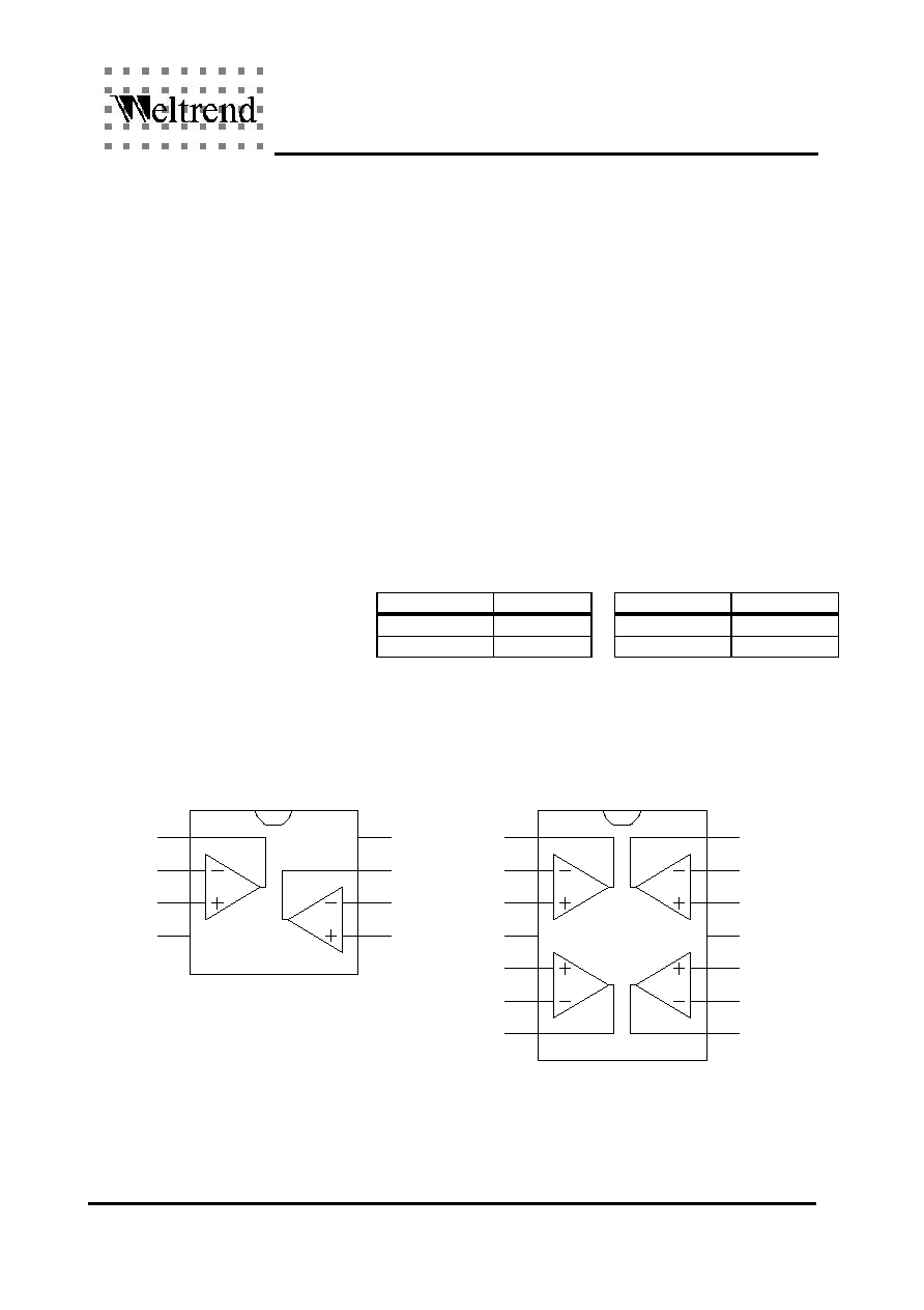
PIN CONFIGURATION
D
D
D
C
C
C
-IN
A
OUT
A
V+
V-
-IN
+IN
OUT
-IN
B
B
B
B
-IN
B
OUT
+IN
14
13
12
11
10
9
8
7
6
5
4
3
2
1
WT274C
B
+IN
V+
A
+IN
OUT
OUT
-IN
-IN
+IN
+IN
V-
OUT
D
C
B
A
8
7
6
5
B
1
2
3
4
WT272C
A
A
A
A
WT272C/WT274C
Data Sheet Rev. 1.1
Weltrend Semiconductor, Inc.
Page 3
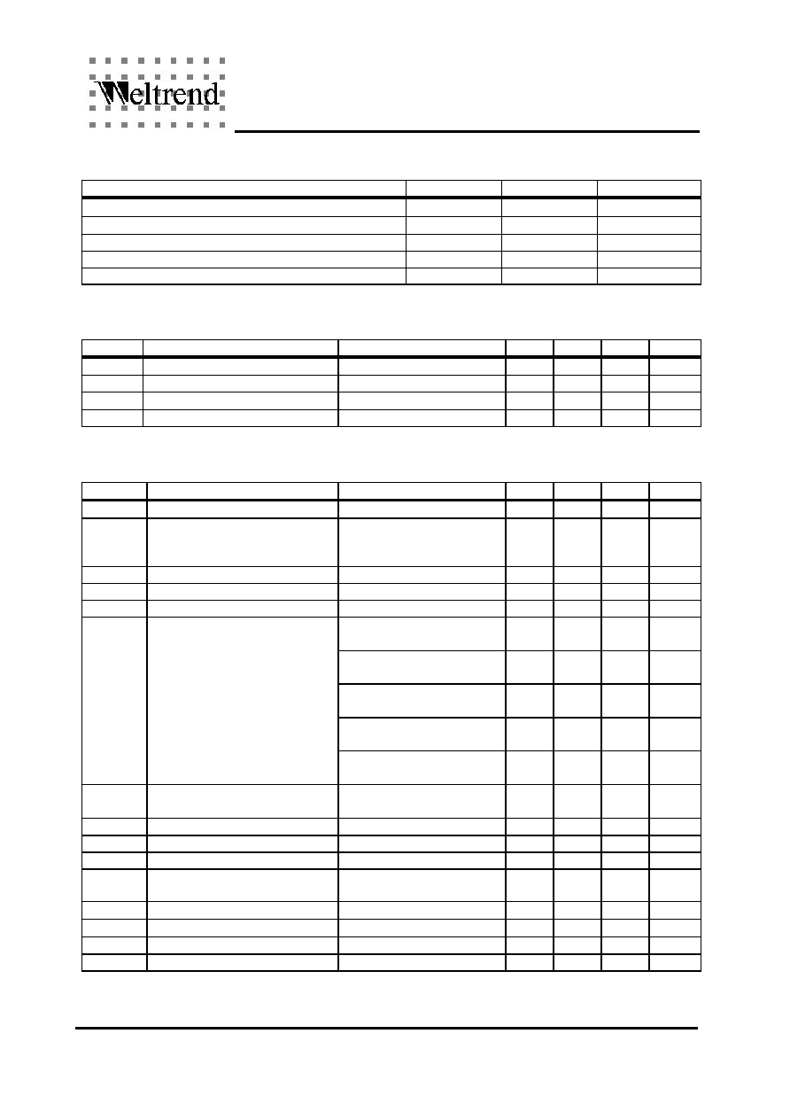
ABSOLUTE MAXIMUM RATINGS
Parameter
Min.
Max.
Units
DC supply voltage (V
+
-
V
-
)
0
8.5
V
Input and output voltage
V
-
- 0.3
V
+
+ 0.3
V
Storage temperature
-65
150
O
C
Ambient temperature with power applied
-20
100
O
C
Duration of output short circuit
Unlimited
*Note: Stresses above those listed may cause permanent damage to the devices
RECOMMENDED OPERATING CONDITION
Symbol
Parameter
Condition
Min.
Typ.
Max.
Units
V
SUPPLY
Supply Voltage
1.2
7
V
I
SOURCE
Output Source Current
5
mA
I
SINK
Output Sink Current
9
µ
A
Ta
Ambient Temperature
0
85
O
C
ELECTRICAL CHARACTERISTICS
(V
+
= 5V, V
-
= 0V, Ta = +25
O
C unless otherwise specified)
Symbol
Parameter
Condition
Min.
Typ.
Max.
Units
V
OS
Input Offset Voltage
2
5
mV
Í
V
OS
/
Í
T Average Temperature
Coefficient of Input Offset
Voltage
0.7
µ
V/
O
C
I
OS
Input Offset Current
1
pA
I
BIAS
Input Bias Current
Ta=25
O
C
1
pA
V
ICOM
Input Common Mode Voltage
0
V+ -1.3
V
Vin =10mV
R
L
=1M
connected to V
-
4.9
4.99
V
Vin =10mV
R
L
=100K
connected to V
-
4.95
V
Vin =10mV
R
L
=10K
connected to V
-
4.75
V
Vin = -10mV
R
L
=1M
, connected to V+
0.5
0.7
V
V
OUT
Output Voltage Swing
Vin = -10mV
R
L
=100K
connected to V+
0.65
V
A
VOL
Large Signal Voltage Gain
V
O
= 1V to 4V, Vi=1.4V
R
L
=1M
20
100
V/mV
GBW
Unit Gain Bandwidth
R
L
=1M
, C
L
=50pF
0.1
MHz
CMRR
Common Mode Rejection Ratio V
O
= 1V, Vi=0 to 3.5V
60
80
dB
PSRR
Power Supply Rejection Ratio
V
O
= 1V
60
90
dB
SR
Slew Rate
A
VOL
=1, C
L
=100pF
V
IN
=5V
P-P
0.03
V/
µ
s
I
SUPPLY
Supply Current (per amplifier)
5
9
µ
A
m
Phase Margin at Unit Gain
R
L
=1M
, C
L
=50pF
55
Degree
e
n
Input Equivalent Noise Voltage
f=1KHz, Rs=100
50
nV/
Hz
V
O1
/V
O2
Channel Separation
A
VOL
=100
120
dB

WT272C/WT274C
Data Sheet Rev. 1.1
Weltrend Semiconductor, Inc.
Page 4
TYPICAL APPLICATION CIRCUIT
Voltage Follower
Instrument Amplifier
VOUT
V
100K
1M
1M
1M
INPUT
V+
1M
100K
100K
100K
50K
500K