
WT6016
Digital Monitor Controller
Ver. 1.51 Jul-31-1998
Weltrend Semiconductor, Inc.
1
GENERAL DESCRIPTION
The WT6016 is a member of WT60XX microcontroller family. It is specially designed for digital
controlled multi-sync monitor. It contains 8-bit CPU, 16K bytes ROM, 288 bytes RAM, 14 PWMs,
parallel I/O, SYNC processor, timer, one DDC interface (slave mode I
2
C interface with DDC1), one
master/slave I
2
C interface, two 4-bit A/D convertors and watch-dog timer.
FEATURES
* 8-bit 6502 compatible CPU, 4MHz operating frequency
* 16384 bytes ROM, 288 bytes SRAM
* 8MHz crystal oscillator
* 14 channels 8-bit/62.5kHz PWM outputs (8 open drain outputs & 6 CMOS outputs)
* Sync signal processor with H+V separation, frequency calculation, H/V polarity detection/control
* Three free-running sync signal outputs for burn-in test (64kHz/62.5Hz, 48kHz/75Hz, 31kHz/60Hz)
* Self-test pattern generator generates cross hatch picture
* DDC interface supports VESA DDC1/DDC2B standard
* Master/slave I
2
C interface
* Watch-dog timer (0.524 second)
* Maximum 25 programmable I/O pins
* One 8-bit programmable timer
* Two 4-bit A/D converter
* One external interrupt request
* Built-in low V
DD
voltage reset
* +5V power supply
PIN ASSIGNMENT
*
I2C is a trademark of Philips Corporation.
*
DDC is a trademark of Video Electronics Standard Association (VESA).
41
42
40
39
38
37
36
35
34
33
32
31
30
29
28
27
26
25
24
23
22
21
20
19
18
17
16
15
14
13
12
11
10
9
8
7
6
5
4
3
2
1
DA0
DA1
DA2
DA3
DA4
DA5
DA6
DA7
GND
HSYNC
OSCI
OSCO
PA0/DA8
PA1/DA9
PA2/DA10
PA3/DA11
PA4/DA12
PA5/DA13
PA6/VSO
PA7/HSO
PB0/HLFO
PB1/HLFI
PB2
PB3/PAT
PB4/SCL2
PB5/SDA2
PB6/IRQ
PC0/AD0
PC1/AD1
PC2
PC3
PC4
PC5
PC6
PC7
SCL1/PD0
SDA1/PD1
VDD
VSYNC
RESET
42-Pin SDIP
40-Pin PDIP
WT6016
Digital Monitor Controller
Ver. 1.51 Jul-31-1998
Weltrend Semiconductor, Inc.
2
PIN DESCRIPTION
Pin No.
40 42
Pin Name
I/O
Descriptions
1
1
DA2
O
D/A converter 2. Open-drain output. External applied voltage can up to 10V.
2
2
DA1
O
D/A converter 1. Open-drain output. External applied voltage can up to 10V.
3
3
DA0
O
D/A converter 0. Open-drain output. External applied voltage can up to 10V.
4
4
/RESET
I
Reset. Active low. Schmitt trigger input with internal pull high.
5
5
VDD
Power supply (+5V).
6
7
GND
Ground (0V).
7
8
OSCO
O
Oscillator Output. Connects a 8MHz crystal.
8
9
OSCI
I
Oscillator Input. Connects a 8MHz crystal.
9
10
PB5/SDA2
I/O
I/O Port B5 or I
2
C data pin. This pin can be an I/O port or I
2
C serial data pin.
10
11
PB4/SCL2
I/O
I/O Port B4 or I
2
C clock pin. This pin can be I/O port or I
2
C clock pin.
11
12
PB3/PAT
I/O
I/O Port B3 or self-test pattern output. When as an I/O port, it is same as PB2.
When it is configured to test pattern output, a vedio signal is output.
12
13
PB2
I/O
I/O Port B2. When it is an input pin, it has an internal pull-up resistor. When it is
an output pin, the source/sink current is 5mA
13
14
PB1/HLFI
I/O
I/O Port B1 or half frequency input.
14
15
PB0/HLFO
I/O
I/O Port B0 or half frequency output.
15
16
PB6/IRQ
I/O
I/O Port B6 or Interrupt Request . When as interrupt request input, it has an
internal pull high resistor. When as an I/O port, it is same as PB3.
16
17
PC7
I/O
I/O Port C7. When it is an input pin, it has an internal pull-up resistor. When it is
an output pin, the sink current is 10mA and the source current is 5mA.
17
18
PC6
I/O
I/O Port C6. Same as PC7.
18
19
PC5
I/O
I/O Port C5. Same as PC7.
19
20
PC4
I/O
I/O Port C4. Same as PC7.
20
21
PC3
I/O
I/O Port C3. Same as PC7.
21
22
PC2
I/O
I/O Port C2. Same as PC7.
22
23
PC1/AD1
I/O
I/O Port C1 or A/D converter input 0.
23
24
PC0/AD0
I/O
I/O Port C0 or A/D converter input 1.
24
25
SDA1/PD1
I/O
DDC serial data or I/O Port D1. When it is a DDC interface pin, It is an open-
drain output. When as an I/O port, it is same as Port B.
25
26
SCL1/PD0
I/O
DDC serial clock or I/O Port D0. When it is a DDC interface pin, It is an open-
drain output. When as an I/O port, it is same as Port B.
26
27
PA0/DA8
I/O
I/O Port A0 or D/A converter 8. This pin can be the output of D/A converter 8
(source/sink = 5mA) or an I/O pin (source = -100uA, sink = 5mA).
27
28
PA1/DA9
I/O
I/O Port A1 or D/A converter 9. Same as PA0/DA8.
28
29
PA2/DA10
I/O
I/O Port A2 or D/A converter 10. Same as PA0/DA8.
29
30
PA3/DA11
I/O
I/O Port A3 or D/A converter 11. Same as PA0/DA8.
30
31
PA4/DA12
I/O
I/O Port A4 or D/A converter 12. Same as PA0/DA8.
31
32
PA5/DA13
I/O
I/O Port A5 or D/A converter 13. Same as PA0/DA8.
32
33
PA6/VSO
I/O
I/O Port A6 / VSYNC OUT. This pin can be the output of VSYNC or an I/O pin.
When as an I/O pin, it is same as PA0.
33
34
PA7/HSO
I/O
I/O Port A7 / HSYNC OUT. This pin can be the output of HSYNC or an I/O pin.
When as an I/O pin, it is same as PA0.
34
35
DA7
O
D/A converter 7. Open-drain output. External applied voltage can up to 10V.
35
36
DA6
O
D/A converter 6. Open-drain output. External applied voltage can up to 10V.
36
38
DA5
O
D/A converter 5. Open-drain output. External applied voltage can up to 10V.
37
39
DA4
O
D/A converter 4. Open-drain output. External applied voltage can up to 10V.
38
40
DA3
O
D/A converter 3. Open-drain output. External applied voltage can up to 10V.
39
41
HSYNC
I
HSYNC input. Schmitt trigger input.
40
42
VSYNC
I
VSYNC input. Schmitt trigger input.

WT6016
Digital Monitor Controller
Ver. 1.51 Jul-31-1998
Weltrend Semiconductor, Inc.
3
FUNCTIONAL DESCRIPTION
CPU
The CPU core is 6502 compatible, operating frequency is 4MHz. Address bus is 16-bit and data bus is
8-bit. the non-maskable interrupt (/NMI) of 6502 is changed to maskable interrupt and is defined as
the INT0. The interrupt request (/IRQ) of 6502 is defined as the INT1.
Default stack pointer is 01FFH.
Please refer the 6502 reference menu for more detail.
ROM
16384 bytes maskable ROM is provided for program codes.
Address is located from C000H to FFFFH.
The following addresses are reserved for special purpose :
FFFAH (low byte) and FFFBH (high byte) : INT0 interrupt vector.
FFFCH (low byte) and FFFDH (high byte) : program reset vector.
FFFEH (low byte) and FFFFH (high byte) : INT1 interrupt vector.
RAM
Built-in 288 bytes SRAM, address is located from 0080H to 019FH. Because the initial stack pointer
is 01FFH, so program must set proper stack pointer when program starts. A recommended value is
019FH.
0000H
:
0020H
REGISTERS
0021H
:
007FH
Reserved
0080H
:
019FH
RAM
01A0H
:
BFFFH
Reserved
C000H
:
:
:
FFFFH
ROM
Low VDD Voltage Reset
A VDD voltage detector is built inside the chip. When VDD is below 4.0 volts, the whole chip will be
reset just like power-on-reset.
Note that the 4.0 volts varies with temperature and process. Please refer the electrical characteristics.
WT6016
Digital Monitor Controller
Ver. 1.51 Jul-31-1998
Weltrend Semiconductor, Inc.
4
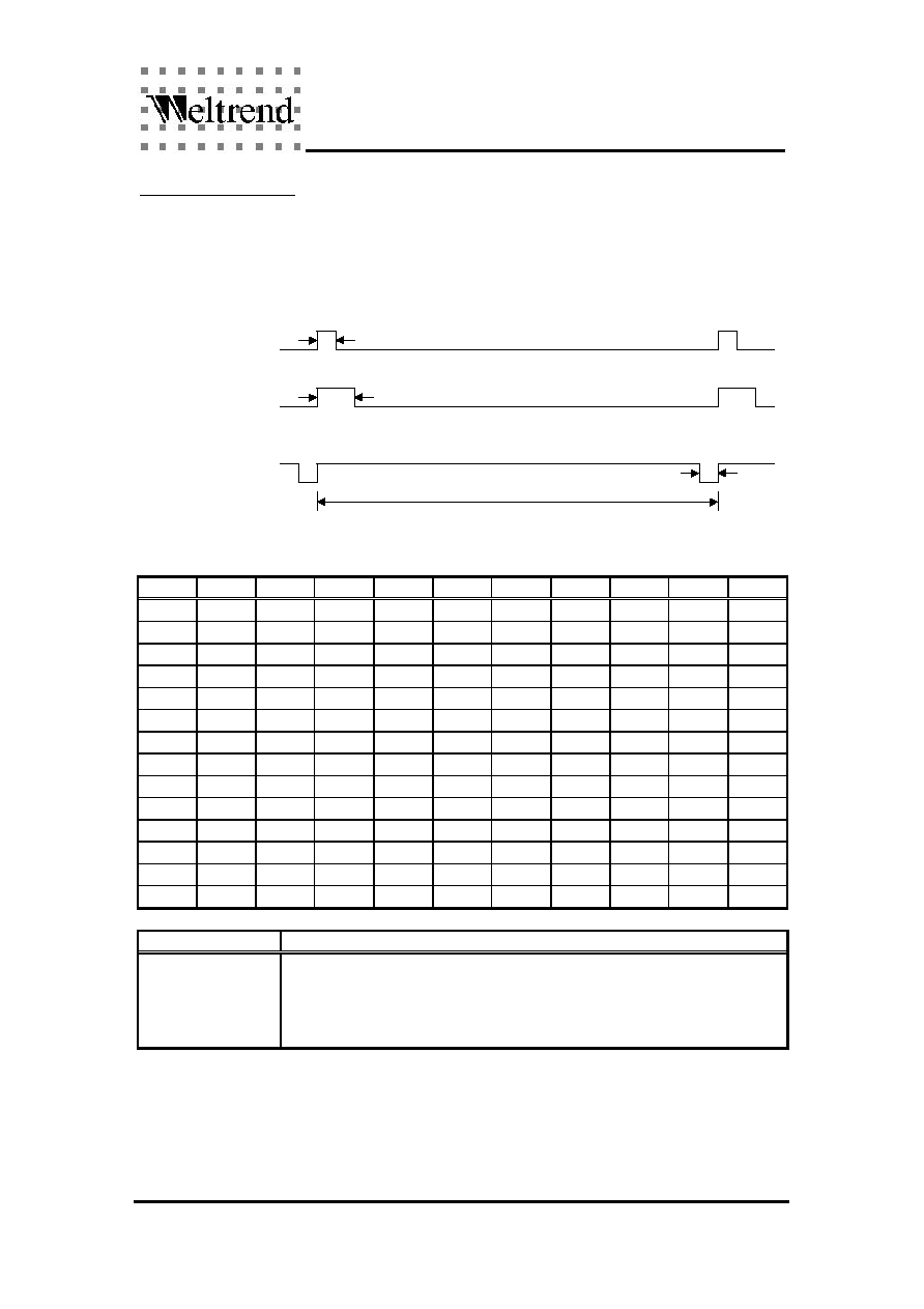
PWM D/A Converter
The WT6018 provides 14 PWM D/A converters. DA0 to DA7 are open-drain outputs and external
applied voltage on these pins can be up to 10 volts. DA8 to DA13 are 5 volts push-pull CMOS outputs
and are shared with I/O Port PA0 to PA5. All D/A converters are 62.5kHz frequency with 8-bit
resolution. Each D/A converter is controlled by the corresponding register (REG#00H to REG#0DH),
the duty cycle can be programmed from 1/256 (data = 01H) to 255/256 (data = FFH).
Duty cycle = 1/256
62.5ns
Duty cycle = 2/256
125ns
62.5ns
Duty cycle = 255/256
1/62.5kHz=16us
To program the PWM D/A converters, write the corresponding registers ( REG#00H to REG#0DH).
Address
R/W
Initial
Bit7
Bit6
Bit5
Bit4
Bit3
Bit2
Bit1
Bit0
0000H
R/W
80H
DA0
7
DA0
6
DA0
5
DA0
4
DA0
3
DA0
2
DA0
1
DA0
0
0001H
R/W
80H
DA1
7
DA1
6
DA1
5
DA1
4
DA1
3
DA1
2
DA1
1
DA1
0
0002H
R/W
80H
DA2
7
DA2
6
DA2
5
DA2
4
DA2
3
DA2
2
DA2
1
DA2
0
0003H
R/W
80H
DA3
7
DA3
6
DA3
5
DA3
4
DA3
3
DA3
2
DA3
1
DA3
0
0004H
R/W
80H
DA4
7
DA4
6
DA4
5
DA4
4
DA4
3
DA4
2
DA4
1
DA4
0
0005H
R/W
80H
DA5
7
DA5
6
DA5
5
DA5
4
DA5
3
DA5
2
DA5
1
DA5
0
0006H
R/W
80H
DA6
7
DA6
6
DA6
5
DA6
4
DA6
3
DA6
2
DA6
1
DA6
0
0007H
R/W
80H
DA7
7
DA7
6
DA7
5
DA7
4
DA7
3
DA7
2
DA7
1
DA7
0
0008H
R/W
80H
DA8
7
DA8
6
DA8
5
DA8
4
DA8
3
DA8
2
DA8
1
DA8
0
0009H
R/W
80H
DA9
7
DA9
6
DA9
5
DA9
4
DA9
3
DA9
2
DA9
1
DA9
0
000AH
R/W
80H
DA10
7
DA10
6
DA10
5
DA10
4
DA10
3
DA10
2
DA10
1
DA10
0
000BH
R/W
80H
DA11
7
DA11
6
DA11
5
DA11
4
DA11
3
DA11
2
DA11
1
DA11
0
000CH
R/W
80H
DA12
7
DA12
6
DA12
5
DA12
4
DA12
3
DA12
2
DA12
1
DA12
0
000DH
R/W
80H
DA13
7
DA13
6
DA13
5
DA13
4
DA13
3
DA13
2
DA13
1
DA13
0
Bit Name
Bit value
DAx7-DAx0
01H : 1/256 duty cycle
02H : 2/256 duty cycle
03H : 3/256 duty cycle
:
FFH : 255/256 duty cycle
** Do not write 00H to the PWM registers. This will cause unstable
output on the corresponding pin.

WT6016
Digital Monitor Controller
Ver. 1.51 Jul-31-1998
Weltrend Semiconductor, Inc.
5
I/O Ports
Port_A :
Pin PA0/DA8 - general purpose I/O shared with DA8 output.
Pin PA1/DA9 - general purpose I/O shared with DA9 output.
Pin PA2/DA10 - general purpose I/O shared with DA10 output.
Pin PA3/DA11 - general purpose I/O shared with DA11 output.
Pin PA4/DA12 - general purpose I/O shared with DA12 output.
Pin PA5/DA13 - general purpose I/O shared with DA13 output.
Pin PA6/VSO - general purpose I/O shared with VSYNC output.
Pin PA7/HSO - general purpose I/O shared with HSYNC output.
Port_A is controlled by REG#10H & REG#11H. In REG#10H, each corresponding bit enables
HSYNC output, VSYNC output or D/A converter output when it is "1". If the corresponding bit is "0",
the output level is decided by REG#11H. In REG#11H, if the I/O corresponding bit (PAn) is "0", the
output is low level (I
OL
=5mA). If PAn bit is "1", the output is high level (I
OH
= -100uA) and can be
used as an input.
Address
R/W
Initial
Bit7
Bit6
Bit5
Bit4
Bit3
Bit2
Bit1
Bit0
0010H
W
00H
EHO
EVO
EDA13 EDA12 EDA11 EDA10
EDA9
EDA8
0011H
W
FFH
PA7W
PA6W
PA5W
PA4W
PA3W
PA2W
PA1W
PA0W
0011H
R
--
PA7R
PA6R
PA5R
PA4R
PA3R
PA2R
PA1R
PA0R
Bit Name
Bit value = "1"
Bit value = "0"
EHO
Enable PA7 as HSYNC output.
PA7 as general purpose I/O.
EVO
Enable PA6 as VSYNC output.
PA6 as general purpose I/O.
EDA13
Enable PA5 as DA13 output.
PA5 as general purpose I/O.
EDA12
Enable PA4 as DA12 output.
PA4 as general purpose I/O.
EDA11
Enable PA3 as DA11 output.
PA3 as general purpose I/O.
EDA10
Enable PA2 as DA10 output.
PA2 as general purpose I/O.
EDA9
Enable PA1 as DA9 output.
PA1 as general purpose I/O.
EDA8
Enable PA0 as DA8 output.
PA0 as general purpose I/O.
PA7W - PA0W
Outputs high level (I
OH
= -100uA).
Outputs low level (I
OL
= 5mA).
PA7R- PA0R
Pin is high level.
Pin is low level.
* If the program wants to force VSYNC output (VSO pin) in low state, write "0" to PA6 bit first, then
write "0" to EVO bit. This is used to prevent high frequency output on VSO pin when the VSYNC
frequency is increased to read EDID data in DDC1 mode.
EDAx
DAx
PAnW
PAnR
Pin PAn
5mA
5mA
100uA