
Weltrend Semiconductor, Inc.
2F, No. 24, Industry E. 9
th
RD., Science-Based Industrial Park, Hsin-Chu, Taiwan
TEL:886-3-5780241 FAX:886-3-5794278.5770419
Email:support@weltrend.com.tw
WT6248
Digital Monitor Controller with USB Function
(ROM Type)
Preliminary Data Sheet
REV. 1.01
Sep. 20, 2001
The information in this document is subject to change without notice.
�
Weltrend Semiconductor, Inc. All Rights Reserved.
WT6248
v1.01
USB Monitor Controller
Weltrend Semiconductor, Inc.
Page 2
GENERAL DESCRIPTION
The WT6248 is a microcontroller for digital controlled monitor with Universal Serial Bus (USB) interface. It
contains an 8-bit CPU, 48K bytes ROM, 1056 bytes RAM, 14 PWMs, parallel I/Os, SYNC signal
processor, timer, DDC1/2B interface, master/slave I
2
C interface, low speed USB device module, 6-bit A/D
converter and watch-dog timer.
FEATURES
�
8-bit 6502 compatible CPU with 6MHz operating frequency
�
48K bytes ROM, 1024 bytes SRAM+32 bytes bit-addressable SRAM
�
12MHz crystal oscillator
�
14 channels 8-bit PWM outputs
�
Sync signal processor with H+V separation, H/V frequency counter, H/V polarity detection/control and
clamp pulse output
�
Six free-running sync signal outputs (Horizontal frequency up to 106KHz 85Hz@1600x1200)
�
Self-test pattern
�
DDC1/2B module for EDID1.3, EDID2.0 and Enhance EDID
�
Fast mode master/slave I
2
C interface (up to 400KHz)
�
Embedded USB function with endpoint 0 and endpoint 1
�
Built-in 3.3V regulator for USB transceiver
�
Watch-dog timer
�
Maximum 28 programmable I/O pins
�
One 8-bit programmable timer
�
6-bit A/D converter with 4 selectable inputs
�
One external interrupt request input
�
Low V
DD
reset
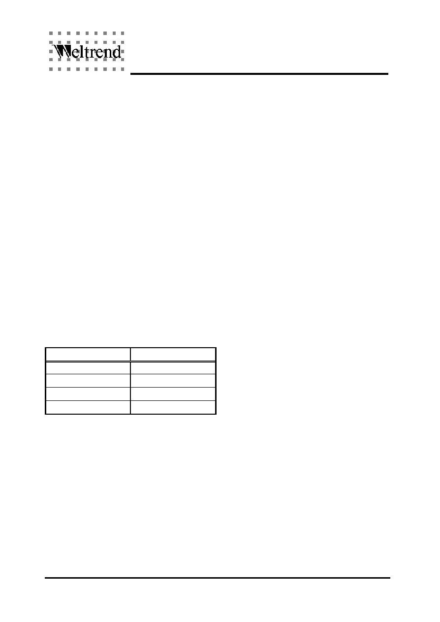
ORDERING INFORMATION
Package Type
Part Number
42-pin PDIP
WT6248-N42
42-pin Shrink PDIP
WT6248-K42
44-pin SOP
WT6248-S44
44-pin PLCC
WT6248-L44

WT6248
v1.01
USB Monitor Controller
Weltrend Semiconductor, Inc.
Page 3
PIN CONFIGURATION
39
38
37
36
35
34
33
32
31
30
29
28
27
26
25
24
23
22
21
20
19
18
1
6
5
4
3
2
44
43
42
41
40
7
17
16
15
14
13
12
11
10
9
8
D+
D-
GND
HIN
IRQ
OSCI
OSCO
PA0/SDA1
PA1/SCL1
PA2/PWM8
PA3/PWM9
PA4/PWM10
PA5/PWM11
PA6/PWM12
PA7/PWM13/CLAMP
PB0/HFO
PB1/HFI
PB2
PB3/PAT
PB4/SCL2
PB5/SDA2
PC0/AD0
PC1/AD1
PC2/AD2
PC3/AD3
PC4
PC5
PC6
PC7/SOGIN
PD0/VOUT
PD1/HOUT
PD2/PWM7
PD3/PWM6
PD4/PWM5
PD5/PWM4
PWM0
PWM1
PWM2
PWM3
RESET/3V3
VDD
VIN
44
43
42
41
40
39
38
37
36
35
34
33
32
31
30
29
28
27
26
25
24
23
22
21
1
20
19
18
17
16
15
14
13
12
11
10
9
8
7
6
5
4
3
2
D+
D-
GND
HIN
IRQ
OSCI
OSCO
PA0/SDA1
PA1/SCL1
PA2/PWM8
PA3/PWM9
PA4/PWM10
PA5/PWM11
PA6/PWM12
PA7/PWM13/CLAMP
PB0/HFO
PB1/HFI
PB2
PB3/PAT
PB4/SCL2
PB5/SDA2
PC0/AD0
PC1/AD1
PC2/AD2
PC3/AD3
PC4
PC5
PC6
PC7/SOGIN
PD0/VOUT
PD1/HOUT
PD2/PWM7
PD3/PWM6
PD4/PWM5
PD5/PWM4
PWM0
PWM1
PWM2
PWM3
RESET/3V3
VDD
VIN
WT6248-L44
WT6248-S44
WT6248-K42
WT6248-N42
44-pin PLCC
44-pin SOP
42-pin PDIP
42-pin SPDIP
WT6248
v1.01
USB Monitor Controller
Weltrend Semiconductor, Inc.
Page 4
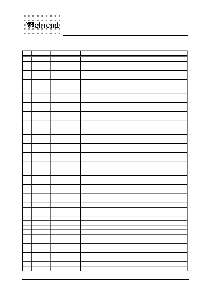
PIN DESCRIPTION
L44 S44 42
Pin Name I/O
Description
1
1
1 D+
I/O USB D+ signal.
2
2
2 PWM2
O PWM2 output (10V open-drain).
3
3
3 PWM1
O PWM1 output (5V open-drain).
4
4
4 PWM0
O PWM0 output (5V open-drain).
5
5
5 /RESET/3V3
I Reset input or +3.3V regulator output for USB transceiver power
6
-
- NC
No Connection.
7
6
6 VDD
+5V power supply.
-
7
- NC
No Connection.
8
8
7 GND
Ground.
9
9
8 OSCO
I/O 12MHz oscillator output.
10
10
9 OSCI
I 12MHz oscillator input.
11
11 10 PB5/ SDA2
I/O Port B5 or I
2
C interface data line.
12
12 11 PB4/ SCL2
I/O Port B4 or I
2
C interface clock line.
13
13 12 PB3/PAT
I/O Port B3 or test pattern output
14
14 13 PB2
I/O Port B2.
15
15 14 PB1/HFI
I/O Port B1 or half frequency divider input.
16
16 15 PB0/HFO
I/O Port B0 or half frequency divider output.
17
17 16 /IRQ
I Interrupt request input. A low level on this can generate interrupt.
18
18 17 PC7/SOGIN I/O Port C7 or Sync on Green input.
19
19 18 PC6
I/O Port C6.
20
20 19 PC5
I/O Port C5.
21
21 20 PC4
I/O Port C4.
22
22 21 PC3/AD3
I/O Port C3 or ADC input 3.
23
23 22 PC2/AD2
I/O Port C2 or ADC input 2.
24
24 23 PC1/AD1
I/O Port C1 or ADC input 1.
25
25 24 PC0/AD0
I/O Port C0 or ADC input 0.
26
26 25 PA0/SDA1
I/O Port A0 or DDC interface SDA pin.
27
27 26 PA1/SCL1
I/O Port A1 or DDC interface SCL pin.
28
28 27 PA2/PWM8 I/O Port A2 or PWM8 output.
29
29 28 PA3/PWM9 I/O Port A3 or PWM9 output.
30
30 29 PA4/PWM10 I/O Port A4 or PWM10 output.
31
31 30 PA5/PWM11 I/O Port A5 or PWM11 output.
32
32 31 PA6/PWM12 I/O Port A6 or PWM12 output.
33
33 32 PA7/PWM13/
CLAMP
I/O Port A7 or PWM13 output or clamp pulse output.
34
34 33 PD0/VOUT
I/O Port D0 or Vsync output.
35
35 34 PD1/HOUT
I/O Port D1 or Hsync output.
36
36 35 PD2/PWM7 I/O Port D2 or PWM7 output.
37
37 36 PD3/PWM6 I/O Port D3 or PWM6 output.
-
38
- NC
No Connection.
38
39 37 PD4/PWM5 I/O Port D4 or PWM5 output.
39
40 38 PD5/PWM4 I/O Port D5 or PWM4 output.
40
41 39 PWM3
I/O PWM3 output (10V open-drain).
41
42 40 HIN
I Hsync Input.
42
43 41 VIN
I Vsync input.
43
-
- NC
No Connection.
44
44 42 D-
I/O USB D- signal.