
Weltrend Semiconductor, Inc.
�24
2
2F, No. 24, Industry E. 9
th
RD., Science-Based Industrial Park, Hsin-Chu, Taiwan
TEL:886-3-5780241 FAX:886-3-5794278.5770419
Email:support@weltrend.com.tw
`
WT7515
GENERAL DESCRIPTION
The WT7515 provides protection circuits, power good output (PGO), fault protection latch (FPOB),
and a protection detector function (PSONB) control. It can minimize external components of switching
power supply systems in personal computer.
The Over / Under Voltage Detector (OVD / UVD) monitors 3.3V, 5V, 12V input voltage level. The Over
Current Detector (OCD) monitor IS33, IS5, IS12 input current sense. When OVD or UVD or OCD detect
the fault voltage level, the FPOB is latched HIGH and PGO go low. The latch can be reset by PSONB go
HIGH. There is 2.4 ms delay time for PSONB turn off FPOB.
When OVD and UVD and OCD detect the right voltage level, the power good output (PGO) will be
issue.
FEATURES
∑ The Over / Under Voltage Detector (OVD / UVD) monitors 3.3V, 5V, 12V input voltage level.
∑ The Over Current Detector (OCD) monitors IS33, IS5, IS12 input current sense.
∑ Both of the power good output (PGO) and fault protection latch (FPOB) are Open Drain Output.
∑ 75 / 300 ms time delay for UVD.
∑ 300 ms time delay for PGO.
∑ 38 ms for PSONB input signal De≠bounce.
∑ 73 us for internal signal De≠glitches.
∑ 2.4 ms time delay for PSONB turn-off FPOB.
PIN ASSIGNMENT AND PACKAGE TYPE
Pin assignment
PGI
GND
FPOB
PSONB
IS12
RI
NC
PGO
VCC
V5
V33
V12
IS33
IS5
14
13
12
11
10
9
8
1
2
3
4
5
6
7
WT7515≠140WT
PGI
GND
FPOB
PSONB
IS12
RI
IS5
PGO
VCC
V5
V33
VCC2
V12
IS33
14
13
12
11
10
9
8
1
2
3
4
5
6
7
WT7515≠141WT
PGI
GND
FPOB
PSONB
IS12
RI
VCC2
PGO
VCC
V5
V33
V12
IS33
IS5
14
13
12
11
10
9
8
1
2
3
4
5
6
7
WT7515≠142WT
WT7515
Weltrend Semiconductor, Inc.
Page 2
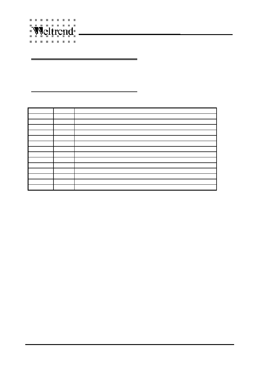
PIN DESCRIPTION
Pin Name
TYPE
Description
PGI
I
Power good input signal pin
GND
P
Ground
FPOB
O
Fault protection output pin, open drain output
PSONB
I
On/Off switch input
IS12
I
12V over current protection sense input
RI
I
Current sense adjust input
VCC2
I
Current sense power supply
IS5
I
5V over current protection sense input
IS33
I
3.3V over current protection sense input
V12
I
12V over/under voltage input pin
V33
I
3.3V over/under voltage input pin
V5
I
5V over/under voltage input pin
VCC
I
Power supply
PGO
O
Power good output signal pin, open drain output
Package type
ORDERING INFORMATION
14≠Pin Plastic DIP WT7515≠N140WT
14≠Pin Plastic SO
WT7515≠S140WT
14≠Pin Plastic DIP WT7515≠N141WT
14≠Pin Plastic SO
WT7515≠S141WT
14≠Pin Plastic DIP WT7515≠N142WT
14≠Pin Plastic SO
WT7515≠S142WT