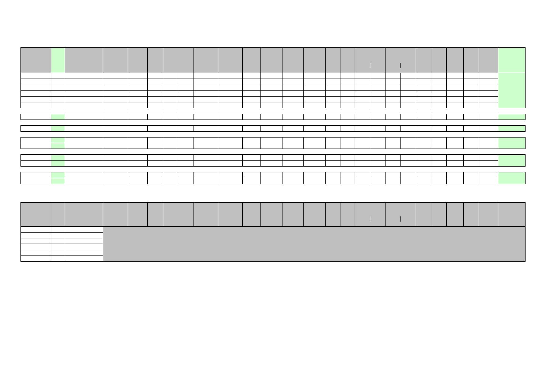
GATE CONTROLLED DEVICE - Gate Turn Off Thyristors - Capsule Type
V
DRM
V
GK
= -
2V
V
RRM
V
RGM
I
T(AV)
T
SINK
= 55
o
C
I
T(RMS)
T
SINK
= 25
o
C
I
TSM(1)
10ms
I
TSM(2)
2ms
I
2
t
V
TM
I
T
= I
TGQM
I
GT
@
25
o
C
V
GT
@
25
o
C
(Typ)
t
on
(min)
t
off
(min)
Rth j-hs
Wt
Mounting
Force
(V)
(V)
(V)
(A)
(
�
�
F)
(A)
(A)
(kA)
(kA)
(kA
2
s)
(V)
(A)
(V)
(
�
�
s)
(A)
(
�
�
s)
(A/
�
�
s)
(
�
�
s)
(
�
�
s)
(K/W)
(g)
(kN)
Notes 1&2
Note 2
Note 2
Note 3
Note 3
Note 4
Note 4
Note 4
Note 5
Note 7
Note 8
WG5025Rx
*
S0500KC250
1200-2500
100-2000
18
500
1
330
640
4
7.2
80 x 10
3
2.5
1.0
0.8
0.4
10
10
20
20.0
90.0
0.065
120
45-90
WG6018Rx
*
S0600KC180
600-1800
100-1400
18
600
1.5
430
870
5
9
130 x 10
3
2.1
1.0
0.8
0.4
12
10
20
20.0
70.0
0.063
120
45-90
WG9014Rx
*
S0900KC140
600-1400
100-1100
18
900
3
445
890
5.5
9.8
150 x 10
3
2.3
1.0
0.8
0.4
15
12
20
20.0
75.0
0.063
120
45-90
WG5025FRx
*
H0500KC250
1200-2500
100-2000
18
500
1
280
540
3
5.4
45 x 10
3
3.2
1.5
0.8
0.8
30
5
40
10.0
60.0
0.065
120
45-90
WG6018FRx
*
H0600KC180
600-1800
100-1400
18
600
1.5
360
700
4
7.2
80 x 10
3
2.6
1.5
0.8
0.8
30
5
40
20.0
45.0
0.063
120
45-90
WG9014FRx
*
H0900KC140
600-1400
100-1100
18
900
3
370
730
4.5
8.1
100 x 10
3
3.0
1.5
0.8
0.8
40
6
40
10.0
50.0
0.063
120
45-90
WG10025SN
Y
G1000LC250
2500
1800
18
1000
2
500
970
5
8.9
125 x 10
3
2.5
1.0
1.0
2.0
20
16
25
2.0
16.0
0.080
170
10-12
101A288
WG10045SN
Y
G1000NC450
4500
1800
18
1000
2
380
750
8
14
80 x 10
3
4.0
1.0
1.2
2.0
20
16
25
2.0
16.0
0.080
480
15-25
Fig. 3
WG20025SN
Y
G2000LC250
2500
1800
18
2000
4
1020
2040
16
24
1.28 x 10
6
2.8
2.5
1.0
5.0
30
24
30
5.0
24.0
0.027
800
17-24
WG20045SN
Y
G2000NC450
4500
1800
18
2000
4
870
1730
13
22
0.85 x 10
6
3.5
2.5
1.0
8.0
30
25
30
8.0
25.0
0.027
800
17-24
WG30025SN
Y
G3000ZC250
2500
1800
18
3000
5
1640
3270
30
40
4.50 x 10
6
2.5
4.0
1.2
7.5
30
28
40
7.5
28.0
0.015
1500
36-44
WG30045SN
Y
G3000ZC450
4500
1800
18
3000
6
1180
2360
24
32
2.88 x 10
6
4.0
3.0
1.0
9.0
30
28
40
9.0
28.0
0.015
1300
36-44
WG30060SN
Y
G3000ZC600
6000
1800
18
3000
3
1100
2300
24
32
2.88 x 10
6
3.5
1.0
1.2
7.5
25
28
70
7.5
28.0
0.015
1500
36-44
WG40045SN
Y
G4000EC450
4500
1800
18
4000
6
1270
2540
25
32
3.1 x 10
6
4.4
4.0
1.2
7.5
50
28
40
7.5
28.0
0.015
1500
36-44
The information contained herein is confidential and is protected by Copyright. The information may not be used or disclosed except with the written permission of and in the manner permitted by the proprietors Westcode Semiconductors Limited. In the interest of product improvement, Westcode reserves the right to change specifications at any time without prior notice.
V
DRM
V
GK
= -
2V
V
RRM
V
GK
I
T(AV)
T
SINK
= 55
o
C
I
T(RMS)
T
CASE
= 25
o
C
I
TSM(1)
10ms
I
TSM(2)
2ms
I
2
t
V
TM
I
T
= I
TGQM
I
GT
@
25
o
C
V
GT
@
25
o
C
(Typ)
t
on
(min)
t
off
(min)
Rth j-hs
Wt
Mounting
Force
(V)
(V)
(V)
(A)
(
�
�
F)
(A)
(A)
(kA)
(kA)
(A
2
s)
(V)
(A)
(V)
(
�
�
s)
(A)
(
�
�
s)
(A/
�
�
s)
(
�
�
s)
(
�
�
s)
(K/W)
(g)
(kN)
Note 1
Note 1
Note 2
Note 3
Note 3
Note 4
Note 4
Note 4
Note 5
Note 7
Note 8
WG5045S
N/A
N/A
WG8045S
N/A
N/A
WG8060S
N/A
N/A
WG7025S
N/A
N/A
WG10025S
N/A
N/A
WG40045S
N/A
N/A
The information contained herein is confidential and is protected by Copyright. The information may not be used or disclosed except with the written permission of and in the manner permitted by the proprietors Westcode Semiconductors Limited. In the interest of product improvement, Westcode reserves the right to change specifications at any time without prior notice.
Notes:
1
V
GK
-2V.
2
Not applicable to this table.
3
Double side cooled, single phase; 50Hz, 180
o
sinewave.
4
T
j(initial)
= 125
o
C, single phase, 180
o
sinewave, re-applied voltage V
D
= V
R
10V.
5
I
T
= 3000A repetitive, I
GM
= 30A, di
GM
/dt = 20A/
�
s, for higher di/dt please consult Westcode Sales Office.
6
With RCD snumber, R = 5 ohms and C is the value as for I
TGQM
7
Does not include snubber discharge time; refers only to minimum time for whole device to be in conduction with anode current di/dt > 10A/
�
s
8
Minimum time to re-fire the device. The gate drive circuit may require a longer period of low impedance option to ensure full extraction of the tail current
Note 6
t
gq
@ di
GQ
/dt
I
T
= I
TGQM
Old Part Number
New Part Number
PDF Data
Sheet
Available
Data Sheet
Available
Outline No.
I
TGQM
@ C
s
Note 6
Note 6
* These products, and their derivatives now undergoing obsolescence - please contact Factory for alternatives.
Part Number
OBSOLETE
New Part Number
(Not applicable)
I
TGQM
@ C
s
t
gt
@ I
GM
I
T
= I
TGQM
Outline No.
t
gt
@ I
GM
I
T
= I
TGQM
Note 6
t
gq
@ di
GQ
/dt
I
T
= I
TGQM
Not for new designs. Please refer to Factory for assistance.
101A296
Fig. 4
Fig. 5
Fig. 6