Document Outline
- Main Menu
- ISD Product Line
- ChipCorder
- ChipCorder Data Sheets
ISD/Winbond ∑ 2727 North First Street, San Jose, CA 95134 ∑ TEL: 408/943-6666 ∑ FAX: 408/544-1787 ∑ http://www.isd.com
August 2000
Figure: ISD4004 Series Block Diagram
GENERAL DESCRIPTION
The ISD4004 ChipCorder
Æ
Products provide high-
quality, 3-volt, single-chip record/playback solu-
tions for 8- to 16-minute messaging applications
which are ideal for cellular phones and other por-
table products. The CMOS-based devices include
an on-chip oscillator, antialiasing filter, smoothing
filter, AutoMuteTM feature, audio amplifier, and
high density, multilevel Flash storage array. The
ISD4004 series is designed to be used in a micro-
processor- or microcontroller-based system. Ad-
dress and control are accomplished through a
Serial Peripheral Interface (SPI) or Microwire Serial
Interface to minimize pin count.
Recordings are stored in on-chip nonvolatile
memory cells, providing zero-power message
storage. This unique, single-chip solution is made
possible through ISD's patented multilevel storage
technology. Voice and audio signals are stored
directly into memory in their natural form, providing
high-quality, solid-state voice reproduction.
ISD4004 Series
Single-Chip Voice Record/Playback Devices
8-, 10-, 12-, and 16-Minute Durations
ISD4004 Series
ii
Voice Solutions in Silicon
TM
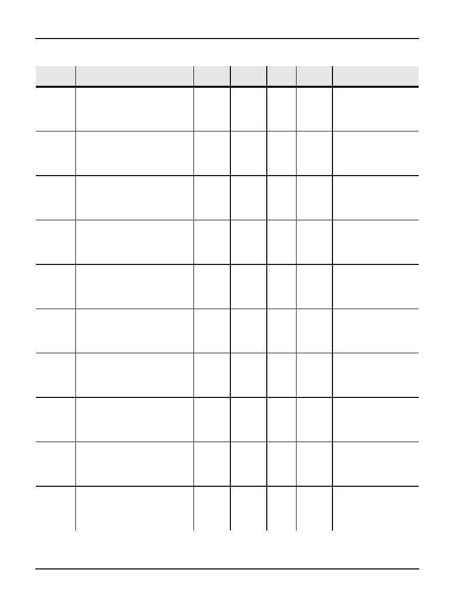
Table: ISD4004 Series Summary
Part
Number
Duration
(minutes)
Input Sample
Rate (KHz)
Typical Filter Pass
Band (KHz)
ISD4004-08M
8.0
8.0
3.4
ISD4004-10M
10.0
6.4
2.7
ISD4004-12M
12.0
5.3
2.3
ISD4004-16M
16.0
4.0
1.7
FEATURES
∑
Single-chip voice record/playback solution
∑
Single +3 volt supply
∑
Low-power consumption
≠ Operating current:
I
CC
Play = 15 mA (typical)
I
CC
Rec = 25 mA (typical)
≠ Standby current: 1 µA (typical)
∑
Single-chip durations of 8, 10, 12, and
16 minutes
∑
High-quality, natural voice/audio reproduction
∑
AutoMute feature provides background noise
attenuation during periods of silence
∑
No algorithm development required
∑
Microcontroller SPI or MicrowireTM Serial
Interface
∑
Fully addressable to handle multiple
messages
∑
Nonvolatile message storage
∑
Power consumption controlled by SPI
or Microwire control register
∑
100-year message retention (typical)
∑
100K record cycles (typical)
∑
On-chip clock source
∑
Available in die form, PDIP, SOIC, and TSOP
∑
Extended temperature (≠20∞C to +70∞C) and
industrial temperature (≠40∞C to +85∞C)
versions available

Table of Contents
ISD
iii
DETAILED DESCRIPTION . . . . . . . . . . . . . . . . . . . . . . . . . . . . . . . . . . . . . . . . . . . . . . . . . . . . . . . . . . . . . . . 1
Speech/Sound Quality . . . . . . . . . . . . . . . . . . . . . . . . . . . . . . . . . . . . . . . . . . . . . . . . . . . . . . . . . . . . 1
Duration . . . . . . . . . . . . . . . . . . . . . . . . . . . . . . . . . . . . . . . . . . . . . . . . . . . . . . . . . . . . . . . . . . . . . . . 1
Flash Storage . . . . . . . . . . . . . . . . . . . . . . . . . . . . . . . . . . . . . . . . . . . . . . . . . . . . . . . . . . . . . . . . . . . 1
Microcontroller Interface . . . . . . . . . . . . . . . . . . . . . . . . . . . . . . . . . . . . . . . . . . . . . . . . . . . . . . . . . . 1
Programming . . . . . . . . . . . . . . . . . . . . . . . . . . . . . . . . . . . . . . . . . . . . . . . . . . . . . . . . . . . . . . . . . . . 1
PIN DESCRIPTIONS . . . . . . . . . . . . . . . . . . . . . . . . . . . . . . . . . . . . . . . . . . . . . . . . . . . . . . . . . . . . . . . . . . . 1
Voltage Inputs (V
CCA
, V
CCD
) . . . . . . . . . . . . . . . . . . . . . . . . . . . . . . . . . . . . . . . . . . . . . . . . . . . . . . . 1
Ground Inputs (V
SSA
, V
SSD
) . . . . . . . . . . . . . . . . . . . . . . . . . . . . . . . . . . . . . . . . . . . . . . . . . . . . . . . . . 1
Non-Inverting Analog Input (ANA IN+) . . . . . . . . . . . . . . . . . . . . . . . . . . . . . . . . . . . . . . . . . . . . . . . . 3
Inverting Analog Input (ANA IN≠) . . . . . . . . . . . . . . . . . . . . . . . . . . . . . . . . . . . . . . . . . . . . . . . . . . . . 3
Audio Output (AUD OUT) . . . . . . . . . . . . . . . . . . . . . . . . . . . . . . . . . . . . . . . . . . . . . . . . . . . . . . . . . . 3
Slave Select (SS) . . . . . . . . . . . . . . . . . . . . . . . . . . . . . . . . . . . . . . . . . . . . . . . . . . . . . . . . . . . . . . . . . 3
Master Out Slave In (MOSI) . . . . . . . . . . . . . . . . . . . . . . . . . . . . . . . . . . . . . . . . . . . . . . . . . . . . . . . . . 3
Master In Slave Out (MISO) . . . . . . . . . . . . . . . . . . . . . . . . . . . . . . . . . . . . . . . . . . . . . . . . . . . . . . . . . 3
Serial Clock (SCLK) . . . . . . . . . . . . . . . . . . . . . . . . . . . . . . . . . . . . . . . . . . . . . . . . . . . . . . . . . . . . . . . 3
Interrupt (INT) . . . . . . . . . . . . . . . . . . . . . . . . . . . . . . . . . . . . . . . . . . . . . . . . . . . . . . . . . . . . . . . . . . . 3
Row Address Clock (RAC) . . . . . . . . . . . . . . . . . . . . . . . . . . . . . . . . . . . . . . . . . . . . . . . . . . . . . . . . . 4
External Clock Input (XCLK) . . . . . . . . . . . . . . . . . . . . . . . . . . . . . . . . . . . . . . . . . . . . . . . . . . . . . . . . 4
AutoMuteTM Feature (AM CAP) . . . . . . . . . . . . . . . . . . . . . . . . . . . . . . . . . . . . . . . . . . . . . . . . . . . . . . 4
SERIAL PERIPHERAL INTERFACE (SPI) DESCRIPTION . . . . . . . . . . . . . . . . . . . . . . . . . . . . . . . . . . . . . . . . . . . . 5
Message Cueing . . . . . . . . . . . . . . . . . . . . . . . . . . . . . . . . . . . . . . . . . . . . . . . . . . . . . . . . . . . . . . . . 5
Power-Up Sequence . . . . . . . . . . . . . . . . . . . . . . . . . . . . . . . . . . . . . . . . . . . . . . . . . . . . . . . . . . . . . 6
SPI Port . . . . . . . . . . . . . . . . . . . . . . . . . . . . . . . . . . . . . . . . . . . . . . . . . . . . . . . . . . . . . . . . . . . . . . . . 7
SPI Control Register . . . . . . . . . . . . . . . . . . . . . . . . . . . . . . . . . . . . . . . . . . . . . . . . . . . . . . . . . . . . . . 7
TIMING DIAGRAMS . . . . . . . . . . . . . . . . . . . . . . . . . . . . . . . . . . . . . . . . . . . . . . . . . . . . . . . . . . . . . . . . . . 14
DEVICE PHYSICAL DIMENSIONS . . . . . . . . . . . . . . . . . . . . . . . . . . . . . . . . . . . . . . . . . . . . . . . . . . . . . . . . 18
ORDERING INFORMATION . . . . . . . . . . . . . . . . . . . . . . . . . . . . . . . . . . . . . . . . . . . . . . . . . . . . . . . . . . . . 23

ISD4004 Series
iv
Voice Solutions in SiliconTM
FIGURES, CHARTS, AND TABLES IN THE ISD4004 SERIES DATA SHEET
Figure 1:
ISD4004 Series TSOP and PDIP/SOIC Pinouts . . . . . . . . . . . . . . . . . . . . . . . . . . . . . . . . 2
Figure 2:
ISD4004 Series ANA IN Modes . . . . . . . . . . . . . . . . . . . . . . . . . . . . . . . . . . . . . . . . . . . 2
Figure 3:
SPI Port . . . . . . . . . . . . . . . . . . . . . . . . . . . . . . . . . . . . . . . . . . . . . . . . . . . . . . . . . . . . . 7
Figure 4:
SPI Interface Simplified Block Diagram . . . . . . . . . . . . . . . . . . . . . . . . . . . . . . . . . . . . 8
Figure 5:
Timing Diagram . . . . . . . . . . . . . . . . . . . . . . . . . . . . . . . . . . . . . . . . . . . . . . . . . . . . . 14
Figure 6:
8-Bit Command Format . . . . . . . . . . . . . . . . . . . . . . . . . . . . . . . . . . . . . . . . . . . . . . 14
Figure 7:
24-Bit Command Format . . . . . . . . . . . . . . . . . . . . . . . . . . . . . . . . . . . . . . . . . . . . . 15
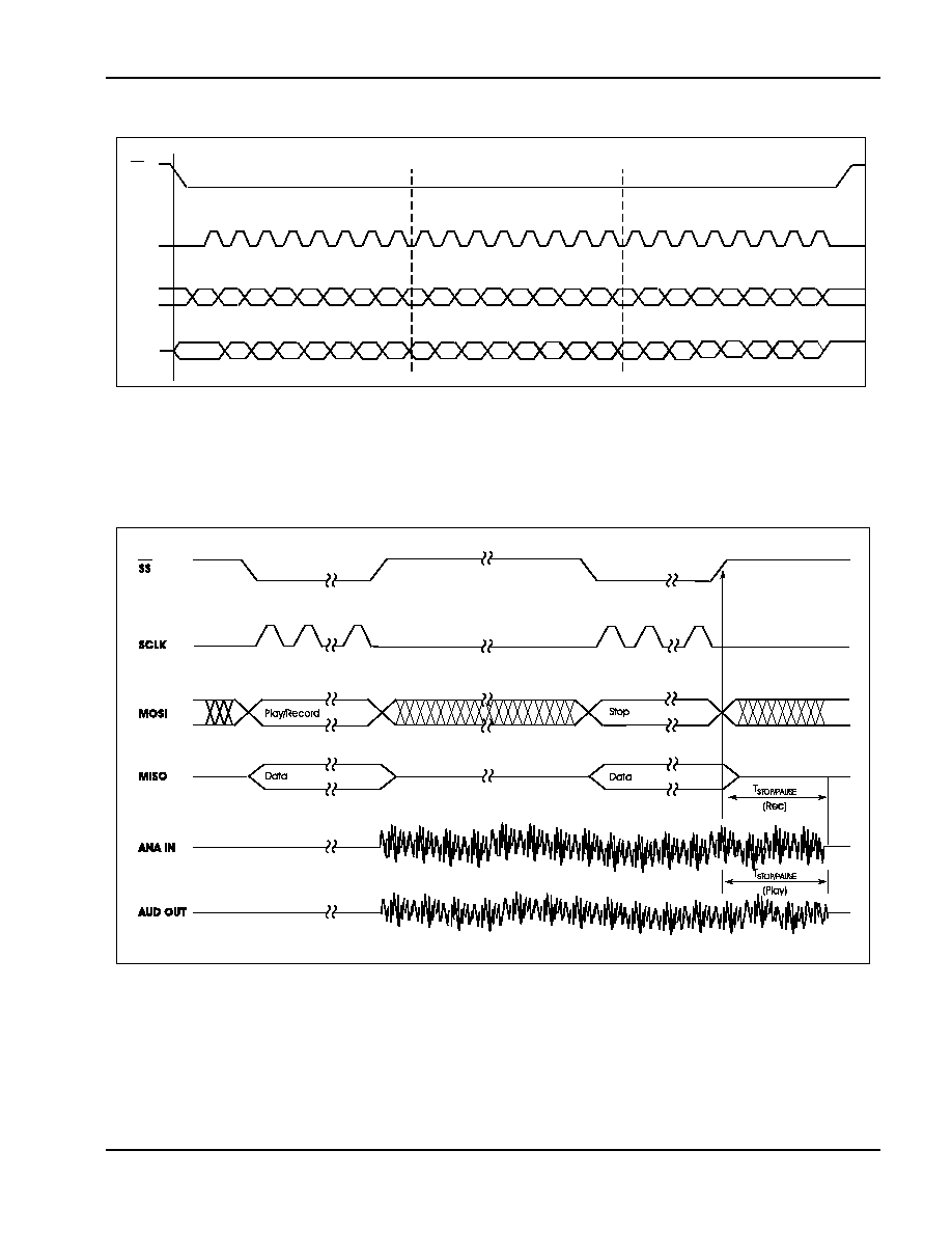
Figure 8:
Playback/Record and Stop Cycle . . . . . . . . . . . . . . . . . . . . . . . . . . . . . . . . . . . . . . . 15
Figure 9:
Application Example Using SPI . . . . . . . . . . . . . . . . . . . . . . . . . . . . . . . . . . . . . . . . . . 16
Figure 10:
Application Example Using Microwire . . . . . . . . . . . . . . . . . . . . . . . . . . . . . . . . . . . . 17
Figure 11:
Application Example Using SPI Port on Microcontroller . . . . . . . . . . . . . . . . . . . . . . . 17
Figure 12:
28-Lead 8x13.4 mm Plastic Thin Small Outline Package (TSOP) Type I (E) . . . . . . . . 18
Figure 13:
28-Lead 0.600-Inch Plastic Dual Inline Package (PDIP) (P) . . . . . . . . . . . . . . . . . . . . 19
Figure 14:
28-Lead 0.300-Inch Plastic Small Outline Integrated Circuit (SOIC) (S) . . . . . . . . . . . 20
Figure 15:
ISD4004 Series Bonding Physical Layout (Unpackaged Die) . . . . . . . . . . . . . . . . . . . 21
Table 1:
External Clock Input Clocking Table . . . . . . . . . . . . . . . . . . . . . . . . . . . . . . . . . . . . . . 4
Table 2:
Opcode Summary . . . . . . . . . . . . . . . . . . . . . . . . . . . . . . . . . . . . . . . . . . . . . . . . . . . 6
Table 3:
SPI Control Register . . . . . . . . . . . . . . . . . . . . . . . . . . . . . . . . . . . . . . . . . . . . . . . . . . . 7
Table 4:
Absolute Maximum Ratings (Packaged Parts) . . . . . . . . . . . . . . . . . . . . . . . . . . . . . . . 8
Table 5:
Operating Conditions (Packaged Parts) . . . . . . . . . . . . . . . . . . . . . . . . . . . . . . . . . . . 8
Table 6:
DC Parameters (Packaged Parts) . . . . . . . . . . . . . . . . . . . . . . . . . . . . . . . . . . . . . . . . 9
Table 7:
AC Parameters (Packaged Parts) . . . . . . . . . . . . . . . . . . . . . . . . . . . . . . . . . . . . . . . . 9
Table 8:
Absolute Maximum Ratings (Die) . . . . . . . . . . . . . . . . . . . . . . . . . . . . . . . . . . . . . . . . 11
Table 9:
Operating Conditions (Die) . . . . . . . . . . . . . . . . . . . . . . . . . . . . . . . . . . . . . . . . . . . . 11
Table 10:
DC Parameters (Die) . . . . . . . . . . . . . . . . . . . . . . . . . . . . . . . . . . . . . . . . . . . . . . . . . 11
Table 11:
AC Parameters (Die) . . . . . . . . . . . . . . . . . . . . . . . . . . . . . . . . . . . . . . . . . . . . . . . . . 12
Table 12:
SPI AC Parameters . . . . . . . . . . . . . . . . . . . . . . . . . . . . . . . . . . . . . . . . . . . . . . . . . . . 13
Table 13:
Plastic Thin Small Outline Package (TSOP) Type I (E) Dimensions . . . . . . . . . . . . . . . . 18
Table 14:
Plastic Dual Inline Package (PDIP) (P) Dimensions . . . . . . . . . . . . . . . . . . . . . . . . . . . 19
Table 15:
Plastic Small Outline Integrated Circuit (SOIC) (S) Dimensions . . . . . . . . . . . . . . . . . . 20
Table 16:
ISD4004 Series Device Pin/Pad Designations, with Respect to Die Center (µm) . . . . 22

ISD4004 Series
1
ISD
DETAILED DESCRIPTION
SPEECH/SOUND QUALITY
The ISD4004 ChipCorder series includes devices
offered at 4.0, 5.3, 6.4, and 8.0 KHz sampling fre-
quencies, allowing the user a choice of speech
quality options. Increasing the duration within a
product series decreases the sampling frequency
and bandwidth, which affects sound quality.
Please refer to the ISD4004 Series Product Summary
table on the second page to compare filter pass
band and product durations.
The speech samples are stored directly into on-chip
nonvolatile memory without the digitization and
compression associated with other solutions. Di-
rect analog storage provides a natural sounding
reproduction of voice, music, tones, and sound
effects not available with most solid-state solu-
tions.
DURATION
To meet end system requirements, the ISD4004 se-
ries products are single-chip solutions at 8, 10, 12,
16 minutes.
FLASH STORAGE
One of the benefits of ISD's ChipCorder technology
is the use of on-chip nonvolatile memory, which pro-
vides zero-power message storage. The message
is retained for up to 100 years (typically) without
power. In addition, the device can be re-record-
ed (typically) over 100,000 times.
MICROCONTROLLER INTERFACE
A four-wire (SCLK, MOSI, MISO, SS) SPI interface is
provided for ISD4004 control and addressing
functions. The ISD4004 is configured to operate as
a peripheral slave device, with a microcontroller-
based SPI bus interface. Read/Write access to all
the internal registers occurs through this SPI inter-
face. An interrupt signal (INT) and internal read-
only Status Register are provided for handshake
purposes.
PROGRAMMING
The ISD4004 series is also ideal for playback-only
applications, where single or multiple message
Playback is controlled through the SPI port. Once
the desired message configuration is created, du-
plicates can easily be generated via an ISD pro-
grammer.
PIN DESCRIPTIONS
VOLTAGE INPUTS (V
CCA
, V
CCD
)
To minimize noise, the analog and digital circuits
in the ISD4004 devices use separate power busses.
These +3 V busses are brought out to separate
pins and should be tied together as close to the
supply as possible. In addition, these supplies
should be decoupled as close to the package as
possible.
GROUND INPUTS (V
SSA
, V
SSD
)
The ISD4004 series utilizes separate analog and
digital ground busses. The analog ground (V
SSA
)
pins should be tied together as close to the pack-
age as possible and connected through a low-
impedance path to power supply ground. The
digital ground (V
SSD
) pin should be connected
through a separate low-impedance path to pow-
er supply ground. These ground paths should be
large enough to ensure that the impedance be-
tween the V
SSA
pins and the V
SSD
pin is less than
3
W. The backside of the die is connected to V
SS
through the substrate resistance. In a chip-on-
board design, the die attach area must be con-
nected to V
SS
or left floating.

ISD4004 Series
2
Voice Solutions in Silicon
TM
Figure 2: ISD4004 Series ANA IN Modes
Figure 1: ISD4004 Series TSOP and PDIP/SOIC Pinouts
28-PIN TSOP
ISD4004
PDIP/SOIC
ISD4004

ISD4004 Series
3
ISD
NON-INVERTING ANALOG INPUT (ANA IN+)
This pin is the non-inverting analog input that trans-
fers the signal to the device for recording. The an-
alog input amplifier can be driven single ended or
differentially. In the single-ended input mode, a
32 mVp-p (peak-to-peak) maximum signal should
be capacitively connected to this pin for optimal
signal quality. This capacitor value, together with
the 3 K
W input impedance of ANA IN+, is selected
to give cutoff at the low frequency end of the
voice passband. In the differential-input mode,
the maximum input signal at ANA IN+ should be
16 mVp-p for optimal signal quality. The circuit
connections for the two modes are shown in Fig-
ure 2 on page 2.
INVERTING ANALOG INPUT (ANA IN≠)
This pin is the inverting analog input that transfers
the signal to the device for recording in the differ-
ential-input mode. In this differential-input mode,
a 16 mVp-p maximum input signal at ANA IN≠
should be capacitively coupled to this pin for op-
timal signal quality as shown in the ISD4004 Series
ANA IN Modes, Figure 2. This capacitor value
should be equal to the coupling capacitor used
on the ANA IN+ pin. The input impedance at ANA IN≠
is nominally 56 K
W. In the single-ended mode, ANA
IN≠ should be capacitively coupled to V
SSA
through a capacitor equal to that used on the
ANA IN+ input.
AUDIO OUTPUT (AUD OUT)
This pin provides the audio output to the user.
It is capable of driving a 5 K
W impedance. It is
recommended that this pin be AC coupled.
NOTE
The AUDOUT pin is always at 1.2 volts when
the device is powered up. When in play-
back, the output buffer connected to this
pin can drive a load as small as 5 KW.
When in record, a resistor connects AUD-
OUT to the internal 1.2 volt analog ground
supply. This resistor is approximately
850 KW, but will vary somewhat according
to the sample rate of the device. This rel-
atively high impedance allows this pin to
be connected to an audio bus without
loading it down.
SLAVE SELECT (SS)
This input, when LOW, will select the ISD4004
device.
MASTER OUT SLAVE IN (MOSI)
This is the serial input to the ISD4004 device. The
master microcontroller places data on the MOSI
line one half-cycle before the rising clock edge to
be clocked in by the ISD4004 device.
MASTER IN SLAVE OUT (MISO)
This is the serial output of the ISD4004 device. This
output goes into a high-impedance state if the
device is not selected.
SERIAL CLOCK (SCLK)
This is the clock input to the ISD4004. It is generat-
ed by the master device (microcontroller) and is
used to synchronize data transfers in and out of
the device through the MISO and MOSI lines. Data
is latched into the ISD4004 on the rising edge of
SCLK and shifted out of the device on the falling
edge of SCLK.
INTERRUPT (INT)
The ISD4004 interrupt pin goes LOW and stays LOW
when an Overflow (OVF) or End of Message (EOM)
marker is detected. This is an open drain output
pin. Each operation that ends in an EOM or Over-
flow will generate an interrupt including the mes-
sage cueing cycles. The interrupt will be cleared
the next time an SPI cycle is initiated. The interrupt
status can be read by an RINT instruction.
Overflow Flag (OVF)--The Overflow flag indi-
cates that the end of the ISD4004's analog mem-
ory has been reached during a record or
playback operation.
End of Message (EOM)--The End-of-Message
flag is set only during playback operation when an
EOM is found. There are eight EOM flag position
options per row.

ISD4004 Series
4
Voice Solutions in Silicon
TM
ROW ADDRESS CLOCK (RAC)
This is an open drain output pin that provides a sig-
nal with a 200 ms period at the 8 KHz sampling fre-
quency. (This represents a single row of memory
and there are 2400 rows of memory in the ISD4004
series devices.) This signal stays HIGH for 175 ms
and stays LOW for 25 ms when it reaches the end
of a row.
The RAC pin stays HIGH for 109.38
msec and stays
LOW for 15.63
msec in Message Cueing mode
(see page 5 for a more detailed description of
Message Cueing). Refer to the AC Parameters ta-
ble for RAC timing information on other sample
rate products.
When a record command is first initiated, the RAC
pin remains HIGH for an extra T
RACLO
period. This is
due to the need to load sample and hold circuits
internal to the device. This pin can be used for
message management techniques.
EXTERNAL CLOCK INPUT (XCLK)
The external clock input for the ISD4004 products
has an internal pull-down device. These products
are configured at the factory with an internal sam-
pling clock frequency centered to ±1 percent of
specification. The frequency is then maintained to
a variation over the entire commercial tempera-
ture and operating voltage ranges as defined by
the minimum/maximum limits in the applicable
AC Parameters table. The internal clock has a tol-
erance, over the extended temperature, industrial
temperature and voltage ranges as defined by the
minimum/maximum limits in the applicable AC
Parameters table. A regulated power supply is
recommended for industrial temperature range
parts. If greater precision is required, the device
can be clocked through the XCLK pin in Table 1.
These recommended clock rates should not be
varied because the antialiasing and smoothing filters
are fixed. Thus, aliasing problems can occur if the
sample rate differs from the one recommended.
The duty cycle on the input clock is not critical, as
the clock is immediately divided by two internally.
If the XCLK is not used, this input should be
connected to ground.
AUTOMUTETM FEATURE (AM CAP)
This pin is used in controlling the AutoMute feature.
The AutoMute feature attenuates the signal when
it drops below an internally set threshold. This helps
to eliminate noise (with 6 dB of attenuation) when
there is no signal (i.e., during periods of silence). A
1
mF capacitor to ground should be connected to
the AM CAP pin. This capacitor becomes a part of
an internal peak detector which senses the signal
amplitude (peak). This peak level is compared to
an internally set threshold to determine the Auto-
Mute trip point. For large signals the AutoMute at-
tenuation is set to 0 dB while 6 dB of attenuation
occurs for silence. The 1
mF capacitor also affects
the rate at which the AutoMute feature changes
with the signal amplitude (or the attack time). The
Automute feature can be disabled by connecting
the AM CAP pin to V
CCA
.
Table 1:
External Clock Input Clocking
Table
Part Number
Sample Rate Required Clock
ISD4004-08M
8.0 KHz
1024 KHz
ISD4004-10M
6.4 KHz
819.2 KHz
ISD4004-12M
5.3 KHz
682.7 KHz
ISD4004-16M
4.0 KHz
512 KHz

ISD4004 Series
5
ISD
SERIAL PERIPHERAL INTERFACE (SPI) DESCRIPTION
The ISD4004 series operates from an SPI serial inter-
face. The SPI interface operates with the following
protocol.
The data transfer protocol assumes that the mi-
crocontroller's SPI shift registers are clocked on the
falling edge of the SCLK. With the ISD4004, data is
clocked in on the MOSI pin on the rising clock
edge. Data is clocked out on the MISO pin on the
falling clock edge.
1. All serial data transfers begin with the falling
edge of SS pin.
2. SS is held LOW during all serial communica-
tions and held HIGH between instructions.
3. Data is clocked in on the rising clock edge
and data is clocked out on the falling clock
edge.
4. Play and Record operations are initiated by
enabling the device by asserting the SS pin
LOW, shifting in an opcode and an address
field to the ISD4004 device (refer to the Op-
code Summary on the page 6).
5. The opcodes and address fields are as fol-
lows: <8 control bits> and <16 address
bits>.
6. Each operation that ends in an EOM or
Overflow will generate an interrupt, includ-
ing the Message Cueing cycles. The Inter-
rupt will be cleared the next time an SPI
cycle is initiated.
7. As Interrupt data is shifted out of the
ISD4004 MISO pin, control and address
data is simultaneously being shifted into
the MOSI pin. Care should be taken such
that the data shifted in is compatible with
current system operation. It is possible to
read interrupt data and start a new opera-
tion within the same SPI cycle.
8. An operation begins with the RUN bit set
and ends with the RUN bit reset.
9. All operations begin with the rising edge
of SS.
MESSAGE CUEING
Message cueing allows the user to skip through
messages, without knowing the actual physical lo-
cation of the message. This operation is used dur-
ing playback. In this mode, the messages are
skipped 1600 times faster than in normal play-
back mode. It will stop when an EOM marker is
reached. Then, the internal address counter will
point to the next message.
ISD4004 Series
6
Voice Solutions in Silicon
TM
1. Message Cueing can be selected only at the
beginning of a play operation.
2. As the Interrupt data is shifted out of the ISD4004,
control and address data is being shifted in. Care
should be taken such that the data shifted in is
compatible with current system operation. It is
possible to read interrupt data and start a new
operation at the same time. See Figure 5 through
Figure 8 for Opcode format.
POWER-UP SEQUENCE
The ISD4004 will be ready for an operation after
T
PUD
(25 ms approximately for 8 KHz sample rate).
The user needs to wait T
PUD
before issuing an opera-
tional command. For example, to play from ad-
dress 00 the following programing cycle should be
used.
Playback Mode
1.
Send POWERUP command.
2.
Wait T
PUD
(power-up delay).
3.
Send SETPLAY command with address 00.
4.
Send PLAY command.
The device will start playback at address 00 and it
will generate an interrupt when an EOM is
reached. It will then stop playback.
Record Mode
1. Send POWERUP command.
2. Wait T
PUD
(power-up delay).
3. Send POWERUP command.
4. Send SETREC command with address 00.
5. Send REC command.
The device will start recording at address 00 and it
will generate an interrupt when an overflow is
reached (end of memory array). It will then stop re-
cording.
Table 2:Opcode Summary
Instruction
Opcode <8 bits>
Address <16 bits>
Operational Summary
POWERUP
00100XXX
Power-Up: Device will be ready for an operation after T
PUD
.
SETPLAY
11100XXX <A15≠A0>
Initiates Playback from address <A15≠A0>.
PLAY
11110XXX
Playback from the current address (until EOM or OVF).
SETREC
10100XXX <A15≠A0>
Initiates a Record operation from address <A15≠A0>.
REC
10110XXX
Records from current address until OVF is reached.
SETMC
11101XXX <A15≠A0>
Initiates Message Cueing (MC) from address <A15≠A0>.
MC
1
11111XXX
Performs a Message Cue. Proceeds to the end of the current
message (EOM) or enters OVF condition if no more messages are
present.
STOP
0X110XXX
Stops current operation.
STOPPWRDN
0X01XXXX
Stops current Operation and enters stand-by (power-down) mode.
RINT
2
0X110XXX
Read Interrupt status bits: Overflow and EOM.
ISD4004 Series
7
ISD
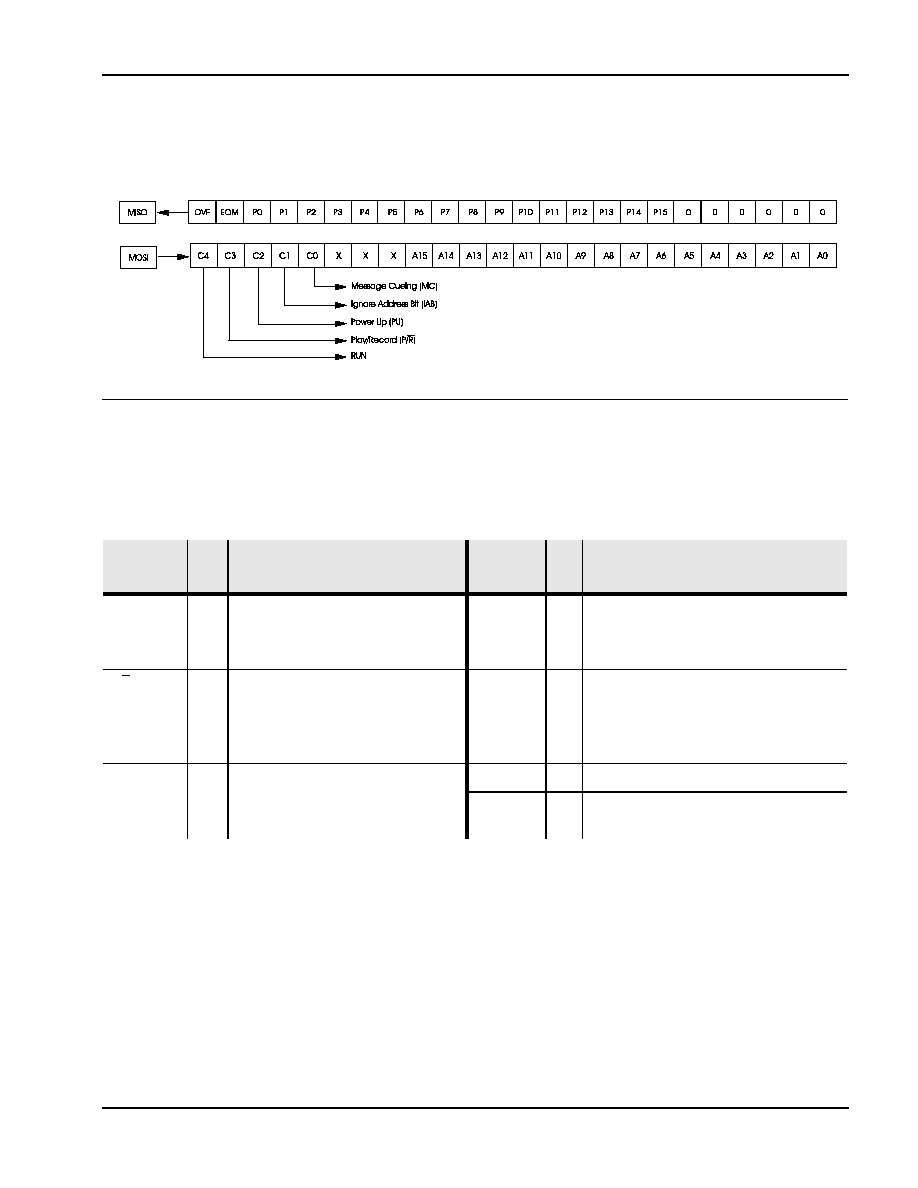
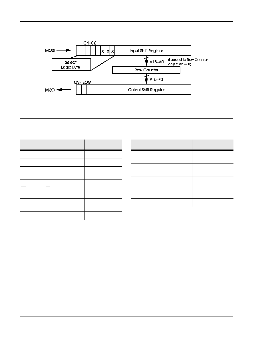
SPI PORT
The following diagram describes the SPI port and the control bits associated with it.
Figure 3: SPI Port
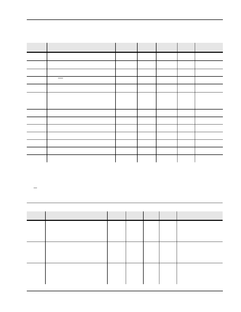
SPI CONTROL REGISTER
The SPI control register provides control of individual device functions such as Play, Record, Message
Cueing, Power-Up and Power-Down, Start and Stop operations, and Ignore Address pointers.
Table 3: SPI Control Register
Control
Register
Bit
Device Function
Control
Register
Bit
Device Function
RUN
Enable or Disable an operation
PU
Master power control
=
=
1
0
Start
Stop
=
=
1
0
Power-Up
Power-Down
P/R
Selects Play or Record operation
IAB
Ignore address control bit
=
=
1
0
Play
Record
=
=
1
0
Ignore input address register (A15≠A0)
Use the input address register contents
for an operation (A15≠A0)
MC
Enable or Disable Message Cueing
P15≠P0
Output of the row pointer register
=
=
1
0
Enable Message Cueing
Disable Message Cueing
A15≠A0
Input address register
ISD4004 Series
8
Voice Solutions in Silicon
TM
1. Stresses above those listed may cause permanent
damage to the device. Exposure to the absolute
maximum ratings may affect device reliability.
Functional operation is not implied at these
conditions.
1. Case temperature.
2. V
CC
= V
CCA
= V
CCD.
3. V
SS
= V
SSA
= V
SSD
.
Table 4:
Absolute Maximum Ratings
(Packaged Parts)
(1)
Condition
Value
Junction temperature
150∞C
Storage temperature range
≠65∞C to +150∞C
Voltage applied to any pin
(V
SS
≠ 0.3 V) to
(V
CC
+ 0.3 V)
Voltage applied to MOSI, SCLK,
INT, RAC and SS pins (input current
limited to ± 20mA
(V
SS
≠ 1.0 V) to
5.5V
Lead temperature
(soldering ≠ 10 seconds)
300∞C
V
CC
≠ V
SS
≠0.3 V to +7.0 V
Table 5:
Operating Conditions
(Packaged Parts)
Condition
Value
Commercial operating
temperature range
(1)
0∞C to +70∞C
Extended operating
temperature
(1)
≠20∞C to +70∞C
Industrial operating
temperature
(1)
≠40∞C to +85∞C
Supply voltage (V
CC
)
(2)
+2.7 V to +3.3 V
Ground voltage (V
SS
)
(3)
0 V
Figure 4: SPI Interface Simplified Block Diagram
ISD4004 Series
9
ISD
1. Typical values: T
A
= 25∞C and 3.0 V.
2. All min/max limits are guaranteed by ISD via electrical testing or characterization. Not all specifications are
100 percent tested.
3. V
CCA
and V
CCD
connected together.
4. SS = V
CCA
= V
CCD
, XCLK = MOSI = V
SSA
= V
SSD
and all other pins floating.
5. Measured with AutoMute feature disabled.
Table 6: DC Parameters (Packaged Parts)
Symbol
Parameters
Min
(2)
Typ
(1)
Max
(2)
Units
Conditions
V
IL
Input Low Voltage
V
CC
x 0.2
V
V
IH
Input High Voltage
V
CC
x 0.8
V
V
OL
Output Low Voltage
0.4
V
I
OL
= 10 µA
V
OL1
RAC, INT Output Low Voltage
0.4
V
I
OL
= 1 mA
V
OH
Output High Voltage
V
CC
≠ 0.4
V
I
OH
= ≠10 µA
I
CC
V
CC
Current (Operating)
-- Playback
-- Record
15
25
30
40
mA
mA
R
EXT
=
•
(3)
R
EXT
=
•
(3)
I
SB
V
CC
Current (Standby)
1
10
µA
(3) (4)
I
IL
Input Leakage Current
±1
µA
I
HZ
MISO Tristate Current
1
10
µA
R
EXT
Output Load Impedance
5
K
W
R
ANA IN+
ANA IN+ Input Resistance
2.2
3.0
3.8
K
W
R
ANA IN≠
ANA IN≠ Input Resistance
40
56
71
K
W
A
ARP
ANA IN+ or ANA IN≠ to AUD OUT Gain
25
dB
(5)
Table 7: AC Parameters (Packaged Parts)
Symbol
Characteristic
Min
(2)
Typ
(1)
Max
(2)
Units
Conditions
F
S
Sampling
Frequency
ISD4004-08M
ISD4004-10M
ISD4004-12M
ISD4004-16M
8.0
6.4
5.3
4.0
KHz
KHz
KHz
KHz
(5)
(5)
(5)
(5)
F
CF
Filter Pass Band
ISD4004-08M
ISD4004-10M
ISD4004-12M
ISD4004-16M
3.4
2.7
2.3
1.7
KHz
KHz
KHz
KHz
3-dB Roll-Off Point
(3) (7)
3-dB Roll-Off Point
(3) (7)
3-dB Roll-Off Point
(3) (7)
3-dB Roll-Off Point
(3) (7)
T
REC
Record Duration
ISD4004-08M
ISD4004-10M
ISD4004-12M
ISD4004-16M
8
10
12
16
min
min
min
min
(6)
(6)
(6)
(6)
ISD4004 Series
10
Voice Solutions in Silicon
TM
1. Typical values: T
A
= 25∞C and 3.0 V.
2. All min/max limits are guaranteed by ISD via electrical testing or characterization. Not all specifications are 100 percent
tested.
3. Low-frequency cut off depends upon the value of external capacitors (see Pin Descriptions).
4. Single-ended input mode. In the differential input mode, V
IN
maximum for ANA IN+ and ANA IN≠ is 16mVp-p.
5. Sampling Frequency can vary as much as ±2.25 percent over the commercial temperature, and voltage ranges,
and ≠6/+4 percent over the extended temperature, industrial temperature and voltage ranges. For greater
stability, an external clock can be utilized (see Pin Descriptions).
6. Playback and Record Duration can vary as much as ±2.25 percent over the commercial temperature and voltage
ranges, and ≠6/+4 percent over the extended temperature, industrial temperature and voltage ranges. For
greater stability, an external clock can be utilized (see Pin Descriptions).
7. Filter specification applies to the antialiasing filter and the smoothing filter. Therefore, from input to output, expect a
6dB drop by nature of passing through both filters.
8. The typical output voltage will be approximately 570mVp-p with V
IN
at 32mVp-p.
9. For optimal signal quality, this maximum limit is recommended.
10. When a record command is sent, T
RAC
= T
RAC
+ T
RACLO
on the first row addressed.
T
PLAY
Playback Duration
ISD4004-08M
ISD4004-10M
ISD4004-12M
ISD4004-16M
8
10
12
16
min
min
min
min
(6)
(6)
(6)
(6)
T
PUD
Power-Up Delay
ISD4004-08M
ISD4004-10M
ISD4004-12M
ISD4004-16M
25
31.25
37.5
50
msec
msec
msec
msec
T
STOP
or
T
PAUSE
Stop or Pause in
Record or Play
ISD4004-08M
ISD4004-10M
ISD4004-12M
ISD4004-16M
50
62.5
75
100
msec
msec
msec
msec
T
RAC
RAC Clock Period
ISD4004-08M
ISD4004-10M
ISD4004-12M
ISD4004-16M
200
250
300
400
msec
msec
msec
msec
(10)
(10)
(10)
(10)
T
RACLO
RAC Clock Low
Time
ISD4004-08M
ISD4004-10M
ISD4004-12M
ISD4004-16M
25
31.25
37.5
50
msec
msec
msec
msec
T
RACM
RAC Clock Period
in Message
Cueing Mode
ISD4004-08M
ISD4004-10M
ISD4004-12M
ISD4004-16M
125
156.3
187.5
250
µsec
µsec
µsec
µsec
T
RACML
RAC Clock Low
Time in Message
Cueing Mode
ISD4004-08M
ISD4004-10M
ISD4004-12M
ISD4004-16M
15.63
19.53
23.44
31.25
µsec
µsec
µsec
µsec
THD
Total Harmonic Distortion
1
2
%
@ 1 KHz
V
IN
ANA IN Input Voltage
32
mV
Peak-to-Peak
(4) (8) (9)
Table 7: AC Parameters (Packaged Parts)
Symbol
Characteristic
Min
(2)
Typ
(1)
Max
(2)
Units
Conditions
ISD4004 Series
11
ISD
1. Stresses above those listed may cause permanent
damage to the device. Exposure to the absolute
maximum ratings may affect device reliability.
Functional operation is not implied at these conditions.
1. V
CC
= V
CCA
= V
CCD
2. V
SS
= V
SSA
= V
SSD
.
Table 8:
Absolute Maximum Ratings (Die)
(1)
Condition
Value
Junction temperature
150∞C
Storage temperature range
≠65∞C to +150∞C
Voltage applied to any pad
(V
SS
≠ 0.3 V) to
(V
CC
+ 0.3 V)
Voltage applied to MOSI, SCLK, INT,
RAC and SS pins (input current
limited to ± 20mA
(V
SS
≠ 1.0 V) to
5.5 V
V
CC
≠ V
SS
≠0.3 V to +7.0 V
Table 9:
Operating Conditions (Die)
Condition
Value
Commercial operating
temperature range
0∞C to +50∞C
Supply voltage (V
CC
)
(1)
+2.7 V to +3.3 V
Ground voltage (V
SS
)
(2)
0 V
1. Typical values: T
A
= 25∞C and 3.0 V.
2. All min/max limits are guaranteed by ISD via electrical testing or characterization. Not all specifications are
100 percent tested.
3. V
CCA
and V
CCD
connected together.
4. SS = V
CCA
= V
CCD
, XCLK = MOSI = V
SSA
= V
SSD
and all other pins floating.
5. Measured with AutoMute feature disabled.
Table 10: DC Parameters (Die)
Symbol
Parameters
Min
(2)
Typ
(1)
Max
(2)
Units
Conditions
V
IL
Input Low Voltage
V
CC
x 0.2
V
V
IH
Input High Voltage
V
CC
x 0.8
V
V
OL
Output Low Voltage
0.4
V
I
OL
= 10 µA
V
OL1
RAC, INT Output Low Voltage
0.4
V
I
OL
= 1 mA
V
OH
Output High Voltage
V
CC
≠ 0.4
V
I
OH
= ≠10 µA
I
CC
V
CC
Current (Operating)
-- Playback
-- Record
15
25
30
40
mA
mA
R
EXT
=
•
(3)
R
EXT
=
•
(3)
I
SB
V
CC
Current (Standby)
1
10
µA
(3) (4)
I
IL
Input Leakage Current
±1
µA
I
HZ
MISO Tristate Current
1
10
µA
R
EXT
Output Load Impedance
5
K
W
R
ANA IN+
ANA IN+ Input Resistance
2.2
3.0
3.8
K
W
R
ANA IN≠
ANA IN≠ Input Resistance
40
56
71
K
W
A
ARP
ANA IN+ or ANA IN≠ to AUDOUT Gain
25
dB
(5)
ISD4004 Series
12
Voice Solutions in Silicon
TM
Table 11: AC Parameters (Die)
Symbol
Characteristic
Min
(2)
Typ
(1)
Max
(2)
Units
Conditions
F
S
Sampling
Frequency
ISD4004-08M
ISD4004-10M
ISD4004-12M
ISD4004-16M
8.0
6.4
5.3
4.0
KHz
KHz
KHz
KHz
(5)
(5)
(5)
(5)
F
CF
Filter Pass Band
ISD4004-08M
ISD4004-10M
ISD4004-12M
ISD4004-16M
3.4
2.7
2.3
1.7
KHz
KHz
KHz
KHz
3dB Roll-Off Point
(3) (6)
3dB Roll-Off Point
(3) (6)
3dB Roll-Off Point
(3) (6)
3dB Roll-Off Point
(3) (6)
T
REC
Record Duration
ISD4004-08M
ISD4004-10M
ISD4004-12M
ISD4004-16M
8
10
12
16
min
min
min
min
(5)
(5)
(5)
(5))
T
PLAY
Playback Duration
ISD4004-08M
ISD4004-10M
ISD4004-12M
ISD4004-16M
8
10
12
16
min
min
min
min
(5)
(5)
(5)
(5)
T
PUD
Power-Up Delay
ISD4004-08M
ISD4004-10M
ISD4004-12M
ISD4004-16M
25
31.25
37.5
50
msec
msec
msec
msec
T
STOP
or
T
PAUSE
Stop or Pause in
Record or Play
ISD4004-08M
ISD4004-10M
ISD4004-12M
ISD4004-16M
50
62.5
75
100
msec
msec
msec
msec
T
RAC
RAC Clock Period
ISD4004-08M
ISD4004-10M
ISD4004-12M
ISD4004-16M
200
250
300
400
msec
msec
msec
msec
(9)
(9)
(9)
(9)
T
RACLO
RAC Clock Low
Time
ISD4004-08M
ISD4004-10M
ISD4004-12M
ISD4004-16M
25
31.25
37.5
50
msec
msec
msec
msec
T
RACM
RAC Clock Period
in Message
Cueing Mode
ISD4004-08M
ISD4004-10M
ISD4004-12M
ISD4004-16M
125
156.3
187.5
250
msec
msec
msec
msec
T
RACML
RAC Clock Low
Time in Message
Cueing Mode
ISD4004-08M
ISD4004-10M
ISD4004-12M
ISD4004-16M
15.63
19.53
23.44
31.25
msec
msec
msec
msec

ISD4004 Series
13
ISD
1. Typical values: T
A
= 25∞C and 3.0 V.
2. All min/max limits are guaranteed by ISD via electrical testing or characterization. Not all specifications are 100
percent tested.
3. Low-frequency cut off depends upon the value of external capacitors (see Pin Descriptions).
4. Single-ended input mode. In the differential input mode, V
IN
maximum for ANA IN+ and ANA IN≠ is 16 mV peak-
to-peak.
5. Sampling Frequency and Duration can vary as much as ±2.25 percent over the commercial temperature and
voltage ranges. For greater stability, an external clock can be utilized (see Pin Descriptions).
6. Filter specification applies to the antialiasing filter and to the smoothing filter.
7. The typical output voltage will be approximately 570 mV peak-to-peak with V
IN
at 32 mV peak-to-peak.
8. For optimal signal quality, this maximum limit is recommended.
9. When a record command is sent, T
RAC
= T
RAC
+ T
RACLO
on the first row addressed.
1. Typical values: T
A
= 25∞C and 3.0 V. Timing measured at 50 percent of the V
CC
level.
2. Tristate test condition.
THD
Total Harmonic Distortion
1
2
%
@ 1 KHz
V
IN
ANA IN Input Voltage
32
mV
Peak-to-Peak
(4) (7) (8)
Table 12: SPI AC Parameters
1
Symbol
Characteristics
Min
Max
Units
Conditions
T
SSS
SS Setup Time
500
nsec
T
SSH
SS Hold Time
500
nsec
T
DIS
Data in Setup Time
200
nsec
T
DIH
Data in Hold Time
200
nsec
T
PD
Output Delay
500
nsec
T
DF
(2)
Output Delay to hiZ
500
nsec
T
SSmin
SS HIGH
1
msec
T
SCKhi
SCLK High Time
400
nsec
T
SCKlow
SCLK Low Time
400
nsec
F
0
CLK Frequency
1,000
KHz
Table 11: AC Parameters (Die)
Symbol
Characteristic
Min
(2)
Typ
(1)
Max
(2)
Units
Conditions

ISD4004 Series
14
Voice Solutions in Silicon
TM
TIMING DIAGRAMS
Figure 5: Timing Diagram
Figure 6: 8-Bit Command Format
ISD4004 Series
15
ISD
Figure 7: 24-Bit Command Format
Figure 8: Playback/Record and Stop Cycle
SS
MOSI
MISO
A6
A7
A8
A9
A10
A11
A12
A13
A14
A15
A0
A1
A2
A3
A4
A5
P4
P5
P6
P7
P8
P9
OVF
EOM
P0
P1
P2
P3
P10
SCLK
BYTE 1
BYTE 2
BYTE 3
P11
P12
P13
P14
P15
P16
X
X
X
X
X
C3
C4
C2
C1
C0
X
X
X

ISD4004 Series
16
Voice Solutions in Silicon
TM
Figure 9: Application Example Using SPI
(1)
1. This application example is for illustration purposes only. ISD makes no representation or warranty that such
application will be suitable for production.
2. Please make sure the bypass capacitor, C2 is as close as possible to the package.

ISD4004 Series
17
ISD
Figure 10: Application Example Using Microwire
(1)
1. This application example is for illustration purposes only. ISD makes no representation or warranty that such
application will be suitable for production.
2. Please make sure the bypass capacitor, C2 is as close as possible to the package.
Figure 11: Application Example Using SPI Port on Microcontroller
(1)
1. This application example is for illustration purposes only. ISD makes no representation or warranty that such
application will be suitable for production.
2. Please make sure the bypass capacitor, C2 is as close as possible to the package.

ISD4004 Series
18
Voice Solutions in Silicon
TM
DEVICE PHYSICAL DIMENSIONS
Figure 12: 28-Lead 8x13.4 mm Plastic Thin Small Outline Package (TSOP) Type I (E)
NOTE:
Lead coplanarity to be within 0.004 inches.
Table 13: Plastic Thin Small Outline Package (TSOP) Type I (E) Dimensions
INCHES
MILLIMETERS
Min
Nom
Max
Min
Nom
Max
A
0.520
0.528
0.535
13.20
13.40
13.60
B
0.461
0.465
0.469
11.70
11.80
11.90
C
0.311
0.315
0.319
7.90
8.00
8.10
D
0.002
0.006
0.05
0.15
E
0.007
0.009
0.011
0.17
0.22
0.27
F
0.0217
0.55
G
0.037
0.039
0.041
0.95
1.00
1.05
H
0∞
3∞
6∞
0∞
3∞
6∞
I
0.020
0.022
0.028
0.50
0.55
0.70
J
0.004
0.008
0.10
0.21

ISD4004 Series
19
ISD
Figure 13: 28-Lead 0.600-Inch Plastic Dual Inline Package (PDIP) (P)
Table 14: Plastic Dual Inline Package (PDIP) (P) Dimensions
INCHES
MILLIMETERS
Min
Nom
Max
Min
Nom
Max
A
1.445
1.450
1.455
36.70
36.83
36.96
B1
0.150
3.81
B2
0.065
0.070
0.075
1.65
1.78
1.91
C1
0.600
0.625
15.24
15.88
C2
0.530
0.540
0.550
13.46
13.72
13.97
D
0.19
4.83
D1
0.015
0.38
E
0.125
0.135
3.18
3.43
F
0.015
0.018
0.022
0.38
0.46
0.56
G
0.055
0.060
0.065
1.40
1.52
1.65
H
0.100
2.54
J
0.008
0.010
0.012
0.20
0.25
0.30
S
0.070
0.075
0.080
1.78
1.91
2.03
q
0∞
15∞
0∞
15∞

ISD4004 Series
20
Voice Solutions in Silicon
TM
Figure 14: 28-Lead 0.300-Inch Plastic Small Outline Integrated Circuit (SOIC) (S)
NOTE:
Lead coplanarity to be within 0.004 inches.
Table 15: Plastic Small Outline Integrated Circuit (SOIC) (S) Dimensions
INCHES
MILLIMETERS
Min
Nom
Max
Min
Nom
Max
A
0.701
0.706
0.711
17.81
17.93
18.06
B
0.097
0.101
0.104
2.46
2.56
2.64
C
0.292
0.296
0.299
7.42
7.52
7.59
D
0.005
0.009
0.0115
0.127
0.22
0.29
E
0.014
0.016
0.019
0.35
0.41
0.48
F
0.050
1.27
G
0.400
0.406
0.410
10.16
10.31
10.41
H
0.024
0.032
0.040
0.61
0.81
1.02
ISD4004 Series
21
ISD
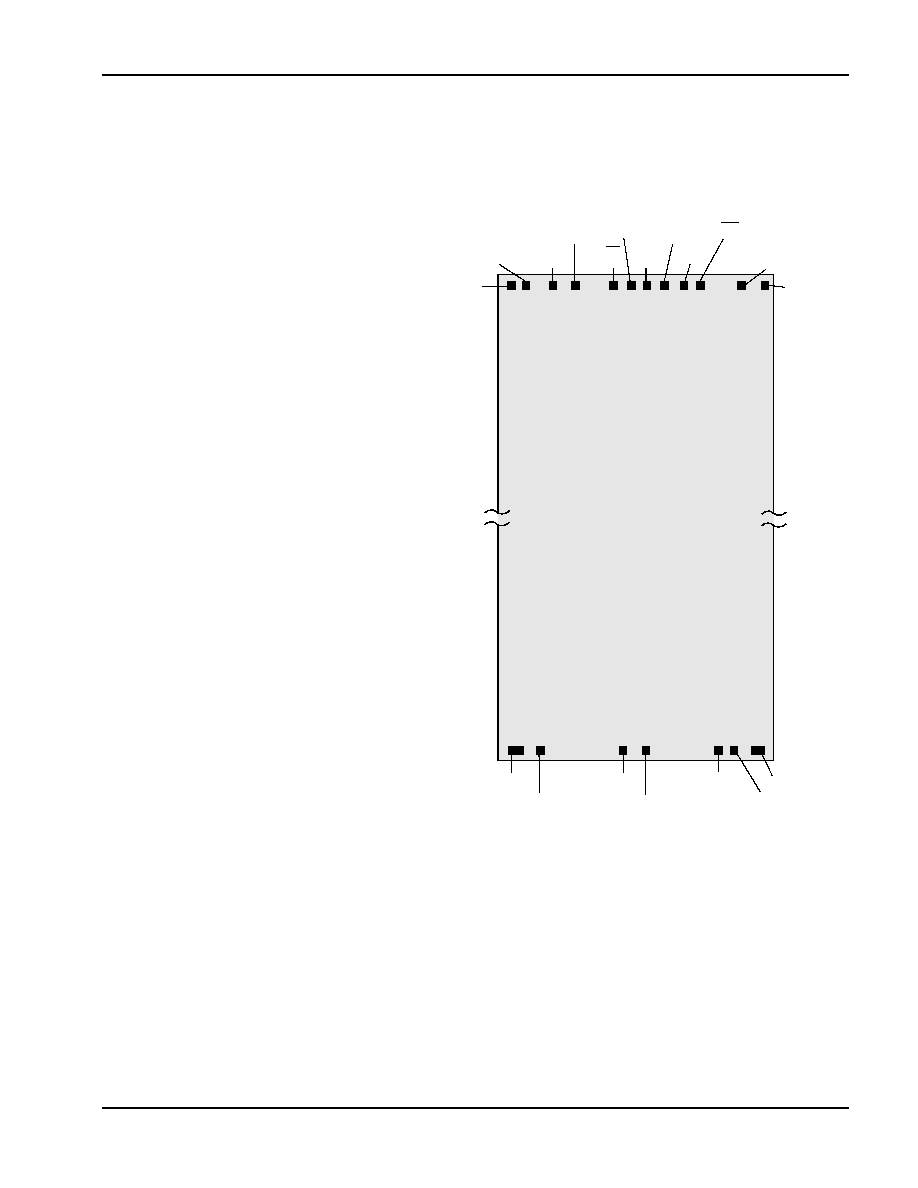
Figure 15: ISD4004 Series Bonding Physical Layout
1
(Unpackaged Die)
1. The backside of die is internally connected to V
SS
. It MUST NOT be connected to any other potential or damage
may occur.
2. Double bond recommended.
3. This figure reflects the current die thickness. Please contact ISD as this thickness may change in the future.
ISD4004 Series
I.
Die Dimensions
X: 4230 microns
Y: 9780 microns
II.
Die Thickness
(3)
11.5 ±0.5 mils
III. Pad Opening (min)
90 x 90 microns
3.5 x 3.5 mils
V
CCD1
V
SSA
AUD OUT
AM CAP
ANA IN≠
INT
V
SSA
XCLK
V
CCD2
SS
MOSI
MISO
V
SSD2
V
SSD1
ISD4004
RAC
SCLK
V
SSA
(2)
ANA IN+
V
CCA
(2)

ISD4004 Series
22
Voice Solutions in Silicon
TM
1. Double bond recommended.
Table 16: ISD4004 Series Device Pin/Pad Designations,
with Respect to Die Center (µm)
Pin
Pin Name
X Axis
Y Axis
V
SSA
V
SS
Analog Power Supply
≠1898.1
≠4622.4
V
SSA
V
SS
Analog Power Supply
≠1599.9
≠4622.4
AUD OUT
Audio Output
281.9
≠4622.4
AM CAP
AutoMute
577.3
≠4622.4
ANA IN ≠
Inverting Analog Input
1449.4
≠4622.4
ANA IN +
Noninverting Analog Input
1603.5
≠4622.4
V
CCA
(1)
V
CC
Analog Power Supply
1898.7
≠4622.4
V
SSA
V
SS
Analog Power Supply
1885.2
≠4622.4
RAC
Row Address Clock
1483.8
4623.7
INT
Interrupt
794.8
4623.7
XCLK
External Clock Input
564.8
4623.7
V
CCD2
V
CC
Digital Power Supply
387.9
4623.7
V
CCD1
V
CC
Digital Power Supply
169.5
4623.7
SCLK
Slave Clock
≠14.7
4623.7
SS
Slave Select
≠198.1
4623.7
MOSI
Master Out Slave In
≠1063.7
4623.7
MISO
Master In Slave Out
≠1325.6
4623.7
V
SSD1
V
SS
Digital Power Supply
≠1655.3
4623.7
V
SSD2
V
SS
Digital Power Supply
≠1836.9
4623.7

ISD4004 Series
23
ISD
ORDERING INFORMATION
When ordering ISD4004 series devices, please refer to the following valid part numbers.
For the latest product information, access ISD's worldwide website at http://www.isd.com.
Part Number
Part Number
Part Number
Part Number
ISD4004-08ME
ISD4004-10ME
ISD4004-12ME
ISD4004-16ME
ISD4004-08MED
ISD4004-10MED
ISD4004-12MED
ISD4004-16MED
ISD4004-08MEI
ISD4004-10MEI
ISD4004-12MEI
ISD4004-16MEI
ISD4004-08MP
ISD4004-10MP
ISD4004-12MP
ISD4004-16MP
ISD4004-08MS
ISD4004-10MS
ISD4004-12MS
ISD4004-16MS
ISD4004-08MSI
ISD4004-10MSI
ISD4004-12MSI
ISD4004-16MSI
ISD4004-08MX
ISD4004-10MX
ISD4004-12MX
ISD4004-16MX
Product Family
ISD4000 Family
Product Series
04
=
Fourth Series (8≠16 min)
Duration:
08M=8 minutes
10M=10 minutes
12M=12 minutes
16M=16 minutes
Special Temperature Field:
Blank=
Commercial Packaged (0∞C to +70∞C)
or
Commercial Die (0∞C to +50∞C)
D
=
Extended (≠20∞C to +70∞C)
I
=
Industrial (≠40∞C to +85∞C)
Package Type:
E
=
28-Lead 8x13.4mm Plastic Thin Small Outline
Package (TSOP) Type 1
P
=
28-Lead 0.600-Inch Plastic Dual Inline Package
(PDIP)
S
=
28-Lead 0.300-Inch Plastic Small Outline Package
(SOIC)
X
=
Die
ISD4004≠ _ _ _ _ _
Product Number Descriptor Key

Part No. 2200998D4004
2727 North First Street
San Jose, California 95134
Tel: 408/943-6666
Fax: 408/544-1787
IMPORTANT NOTICES
The warranty for each product of ISD (Information Storage
Devices, Inc.), is contained in a written warranty which governs
sale and use of such product. Such warranty is contained in the
printed terms and conditions under which such product is sold, or
in a separate written warranty supplied with the product. Please
refer to such written warranty with respect to its applicability to
certain applications of such product.
These products may be subject to restrictions on use. Please
contact ISD, for a list of the current additional restrictions on
these products. By purchasing these products, the purchaser of
these products agrees to comply with such use restrictions. Please
contact ISD for clarification of any restrictions described herein.
ISD, reserves the right, without further notice, to change the ISD
ChipCorder product specifications and/or information in this
document and to improve reliability, functions and design.
ISD assumes no responsibility or liability for any use of the ISD
ChipCorder products. ISD conveys no license or title, either
expressed or implied, under any patent, copyright, or mask work
right to the ISD ChipCorder products, and ISD makes no
warranties or representations that the ISD ChipCorder products are
free from patent, copyright, or mask work right infringement,
unless otherwise specified.
Application examples and alternative uses of any integrated
circuit contained in this publication are for illustration purposes
only and ISD makes no representation or warranty that such
applications shall be suitable for the use specified.
The 100-year retention and 100K record cycle projections are
based upon accelerated reliability tests, as published in the ISD
Reliability Report, and are neither warranted nor guaranteed by
ISD.
Information contained in this ISD ChipCorder data sheet
supersedes all data for the ISD ChipCorder products published
by ISD prior to September, 1998.
This data sheet and any future addendum to this data sheet is
(are) the complete and controlling ISD ChipCorder product
specifications. In the event any inconsistencies exist between the
information in this and other product documentation, or in the
event that other product documentation contains information in
addition to the information in this, the information contained
herein supersedes and governs such other information in its entirety.
Copyright© 1998, ISD (Information Storage Devices, Inc.) All rights
reserved. ISD is a registered trademark of ISD. ChipCorder is a
trademark of ISD. All other trademarks are properties of their
respective owners.