
NX25F011A
NX25F041A
NexFlash Technologies, Inc.
1
PRELIMINARY
NXSF014B-0699
06/11/99
1
2
3
4
5
6
7
8
9
10
11
12
FEATURES
∑ Flash Storage for Resource-Limited Systems
≠ Ideal for portable/mobile and microcontroller-based
applications that store voice, text, and data
∑
NexFlash
Serial Flash Memory
≠ Patented single transistor EEPROM technology
≠ High-density, low-voltage & power, cost-effective
≠ Small 264-byte sectors
≠ 10K/100K write cycles, ten years data retention
∑ Ultra-low Power for Battery-Operation
≠ Single 5V or 3V supply for read and erase/write
≠ 1
µA standby current, 5 mA active @ 3V (typical)
≠ Low frequency read command for very low power
≠ No pre-erase. Erase/Write time of 5 ms/sector
@ 5V ensures efficient battery use
NX25F011A
NX25F041A
1M-BIT AND 4M-BIT SERIAL FLASH MEMORIES
WITH 4-PIN SPI INTERFACE
PRELIMINARY
JUNE 1999
∑ 4-pin SPI Serial Interface
≠ Easily interfaces with popular microcontrollers
≠ Clock operation as fast as 16 MHz
∑ On-chip Serial SRAM
≠ Dual 264-byte Read/Write SRAM buffers
≠ Use in conjunction with or independent of Flash
≠ Off-loads RAM-limited microcontrollers
∑ Special Features for Media-Storage Applications
≠ Byte-level addressing
≠ Transfer and compare sector to SRAM commands
≠ Versatile hardware and software write-protection
≠ Alternate oscillator frequency for EMI sensitive
applications.
≠ In-system electronic part number identification
≠ Removable Serial Flash Module package option
DESCRIPTION
The NX25F011A and NX25F041A Serial Flash memories
provide a storage solution for systems limited in power, pins,
space, hardware, and firmware resources. They are ideal
for applications that store voice, text, and data in a portable
or mobile environment. Using
NexFlash's patented single
transistor EEPROM cell, the devices offer a high-density,
low-voltage, low-power, and cost-effective non-volatile
memory solution. The devices operate on a single 5V or 3V
(2.7V-3.6V) supply for Read and Erase/Write with typical
current consumption as low as 5 mA active and less than
1
µA standby. Sector erase/write speeds as fast as 5 ms
increase system performance, minimize power-on time,
and maximize battery life.
The NX25F011A and NX25F041A provide 1M-bit and
4M-bit of flash memory organized as 512 and 2048 sectors
of 264 bytes each. Each sector is individually addressable
through basic serial-clocked commands. The 4-pin SPI serial
interface works directly with popular microcontrollers.
Special features include: on-chip serial SRAM, byte-level
addressing, double-buffered sector writes, transfer/compare
sector to SRAM, hardware and software write protection,
alternate oscillator frequency, electronic part number, and
removable Serial Flash Module package option. Develop-
ment is supported with the PC-based Serial Flash
Development Kit.
This document contains PRELIMINARY INFORMATION. NexFlash reserves the right to make changes to its product at any time without notice in order to improve design and supply the best
possible product. We assume no responsibility for any errors which may appear in this publication.
Copyright 1998, NexFlash Technologies, Inc.

2
NexFlash Technologies, Inc.
PRELIMINARY
NXSF014B-0699
06/11/99
NX25F011A
NX25F041A
FUNCTIONAL OVERVIEW
An architectural block diagram of the NX25F011A and
NX25F041A is shown in Figure 2. Key elements of the
architecture include:
∑
SPI Interface and Command Set Logic
∑
Serial Flash Memory Array
∑
Serial SRAM and Program Buffer
∑
Write Protection Logic
∑
Configuration and Status Registers
∑
Device Information Sector
Figure 2. NX25F011A and NX25F041A Architectural Block Diagram
DEVICE INFORMATION SECTOR
(READ ONLY)
WRITE PR
O
TECT LOGIC
NexFlash
1 AND 4 MEGABIT
SERIAL FLASH MEMORY ARRAY
512 AND 2048 BYTE-ADDRESSABLE
SECTORS OF 264 BYTES EACH
R
O
W DECODE (512 AND 2048 SECT
ORS)
PROGRAM BUFFER
(264 BYTES)
2112
2112
8
8
8
SRAM
(264 BYTES)
COLUMN DECODE, SENSE AMP LATCH
AND DATA COMPARE LOGIC
HIGH-VOLTAGE
GENERATORS
SECTOR-ADDRESS
LATCH
DATA
9/10/11
WRITE CONTROL
LOGIC
HOLD OR
READ/BUSY
LOGIC
CONFIGURATION
REGISTER
STATUS
REGISTER
SPI
COMMAND
AND
CONTROL
LOGIC
BYTE-ADDRESS
LATCH/COUNTER
9
16
NX25F011A
NX25F041A
NexFlash Technologies, Inc.
3
PRELIMINARY
NXSF014B-0699
06/11/99
1
2
3
4
5
6
7
8
9
10
11
12
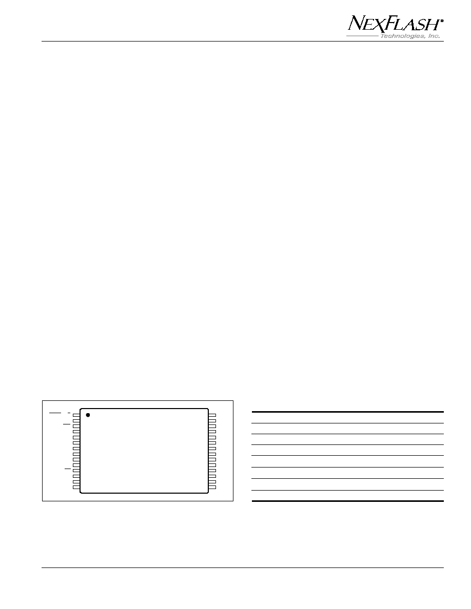
Table 1. Pin Descriptions
SI
Serial Data Input
SO
Serial Data Output
SCK
Serial Clock Input
CS
Chip Select Input
WP
Write Protect Input
Hold, R/B
Hold Input or Read Busy Output
Vcc
Power Supply
GND
Ground
Pin Descriptions
Package
The NX25F011A and NX25F041A are available in a 28-pin
TSOP (Type I) surface mount package. See Figure 3 and
Table 1 for pin assignments. All interface and supply pins
are on one side of the package. The "No Connect" (NC)
pins are not connected to the device, allowing the pads and
the area around them to be used for routing PCB system
traces. The devices are also available in a cost-effective
and space-efficient removable Serial Flash Module
package (see NX25Mxxx data sheet).
Serial Data Input (SI)
The SPI bus Serial Data Input (SI) provides a means for
data to be written to (shifted into) the device.
Serial Data Output (SO)
The SPI bus Serial Data Output (SO) provides a means for
data to be read from (shifted out of) the device during a read
operation. When the device is deselected (
CS=1 or
HOLD=0) the SO pin is in a high-impedance state.
Serial Clock (SCK)
All commands and data written to the Serial Input (SI) are
clocked relative to the rising edge of the Serial Clock
(SCK). By default all data read from the Serial Data Output
(SO) is clocked relative to the falling edge of SCK, allowing
compatibility with standard SPI systems. The user may
specify reading relative to the rising edge of SCK by chang-
ing the setting of the RCE bit in the Configuration Register
(see Figure 6). Clock rates of up to 16 MHz for 5V devices
and up to 8 MHz for 3V devices are supported.
Chip Select (
CS
CS
CS
CS
CS)
The NX25F011A and NX25F041A are selected for opera-
tion when the Chip Select input (
CS) is asserted low. Upon
power-up, an initial low-to-high transition of
CS is required
before any command sequence will be acknowledged. The
device can be deselected to a non-active state when
CS is
brought high. Once deselected, the SO pin will enter a
high-impedance state and power consumption will
decrease to standby levels unless programming is in
process, in which case standby will resume when program-
ming is complete.
Write Protect (
WP
WP
WP
WP
WP)
The Write Protect input (
WP) works in conjunction with the
write protect range set in the configuration register bits.
When
WP is asserted (active low) the entire Flash memory
array is write protected. When high, any Flash memory
sector can be written to unless its address is within the write
protect range that is set in the configuration register.
Hold or Ready/Busy (
HOLD
HOLD
HOLD
HOLD
HOLD or R/B
B
B
B
B)
This multi-function pin can serve either as a
Hold input (
HOLD) or as a Ready-Busy output (R/B).
Factory-programmed as a no connect, the pin can be
reconfigured as a Ready-Busy output or as a Hold input by
setting the configuration register. Warning: this pin is tied
low in the Serial Flash Module and must be left as a no
connect (NC).
Power Supply Pins (Vcc and GND)
The NX25F011A and NX25F041A support single power
supply Read and Erase/Write operations in 5V and 3V
versions. Typical active power is as low as 5 mA for the 3V
version with standby current less than 1
µA.
Figure 3. NX25F011A and NX25F041A
Pin Assignments, 28-Pin TSOP (Type I)
HOLD-R/B
NC
WP
NC
NC
VCC
GND
NC
NC
NC
CS
SCK
SI
SO
NC
NC
NC
NC
NC
NC
NC
NC
NC
NC
NC
NC
NC
NC
1
2
3
4
5
6
7
8
9
10
11
12
13
14
28
27
26
25
24
23
22
21
20
19
18
17
16
15

4
NexFlash Technologies, Inc.
PRELIMINARY
NXSF014B-0699
06/11/99
NX25F011A
NX25F041A
Serial Flash Memory Array
The Flash memory array of the NX25F011A and
NX25F041A are organized as 512 and 2048 sectors of
264-bytes (2,112 bits) each, as shown in Figure 4. Group-
ing sectors as pairs offers a convenient format for applica-
tions that store and transfer data in a DOS compatible
sector size of 512-bytes. The additional 16-bytes per
sector pair can be used for sector management such as
header, checksum, CRC, or other related application
requirements.
The Serial Flash memory of the NX25F011A and
NX25F041A is byte-addressable. That is, each sector is
individually addressable and each byte within a sector is
individually addressable. This allows a single byte, or
specified sequence of bytes, to be read without having to
clock an entire 264-byte sector out of the device. Data can
be read directly from a sector in the Flash memory array
by using a
Read from Sector command from the SPI bus.
Data can be written to a sector in the Flash memory array
using a
Write to Sector command or a Transfer SRAM to
Sector command.
After a sector has been written, the memory array will
become busy while it is programming the specified
non-volatile memory cells of that sector. This busy time will
not exceed t
WP
(~5 ms for 5V devices), during which time
the Flash array is unavailable for read or write access. The
device can be tested to determine the array's availability
by reading the Ready/Busy status, by reading the status
register, or by testing the Ready/Busy pin. Note that the
SRAM is always available, even when the memory array
is busy. See the Serial SRAM section for more details.
The NX25F011A and NX25F041A do not require pre-erase.
The device incorporates an auto-erase-before-write
feature that automatically erases the addressed sector at
the beginning of the write operation. This allows for fast
and consistent programming times and simplifies firm-
ware support by eliminating the need for a separate pre-
erase algorithm and the complex management of dispro-
portional erase and write block sizes commonly found in
other devices.
Byte 0
000H
Sector 0
000H
25F011
S[8:0]
25F041
S[10:0]
Sector Address:
Byte Address: B[8:0]
Sector 1
001H
Sector 2047
7FFH
Sector 511
1FFH
Sector 2046
7FEH
Sector 510
1FEH
Sector 2-2045
002H-7FDH
Sector 2-509
002H-1FDH
Byte1
001H
Byte1
001H
Byte 2-261
002H-105H
Byte 2-261
002H-105H
1M-bit or 4M-bit Serial Flash Memory Array
512 and 2048 Byte-Addressable Sectors
of 264-Bytes each
Byte 262
106H
Byte 262
106H
Byte 263
107H
Byte 0
000H
Byte 263
107H
Byte 0
000H
Byte 0
000H
Byte 1
001H
Byte 1
001H
Byte 2-261
002H-105H
Byte 2-261
002H-105H
Byte 262
106H
Byte 262
106H
Byte 263
107H
Byte 263
107H
Sector 1
001H
Sector 0
000H
Figure 4. NX25F011A and NX25F041A Serial Flash Memory Array

NX25F011A
NX25F041A
NexFlash Technologies, Inc.
5
PRELIMINARY
NXSF014B-0699
06/11/99
1
2
3
4
5
6
7
8
9
10
11
12
Serial SRAM and Program Buffer
One of the most powerful features of the NX25F011A and
NX25F041A is the integrated Serial SRAM and its associ-
ated Program Buffer. Together, the 264-byte Serial SRAM
and 264-byte Program Buffer provide up to 528-bytes of
usable SRAM storage. The SRAM can be used in
conjunction with the Flash memory or independently.
The main purpose of the Serial SRAM is to serve as the
primary buffer for data to be written into the Serial Flash
memory array. Using the
Write to Sector command, data
is first shifted into the SRAM from the SPI bus. When the
command sequence has been completed, the entire
264-bytes is transferred to the Program Buffer. The
Program Buffer supports the array during the
Erase/Write cycle (
t
WP
), freeing the SRAM to accept
new data. This double-buffering scheme increases
erase/write transfer rates and can eliminate the need for
external RAM buffers (Figure 5).
The SRAM is fully byte-addressable. Thus, the entire
264-bytes, a single byte, or a sequence of bytes can be
read from or written to the SRAM. This allows the SRAM to
be used as a temporary work area for read-modify-write
operations prior to a sector write.
The
Transfer Sector to SRAM command allows the con-
tents of a specified sector of Flash memory to be moved to
the SRAM. This can be useful when only a portion of a sector
needs to be altered. In this case the sector is first transferred
to the SRAM, where modifications are made using the
Write
to SRAM command. Once complete, a Transfer SRAM to
Sector command is used to update the sector.
SPI
COMMAND
AND
CONTROL
LOGIC
SCK
CS
SI
SO
STATUS
REGISTER
CONFIGURATION
REGISTER
PROGRAM BUFFER
COMPARE SECTOR
TO SRAM
READ FROM
DEVICE INFORMATION
SECTOR
READ FROM
PROGRAM BUFFER
Note:
1.
A single byte, several bytes, or all bytes of a Flash sector, the SRAM, or Program Buffer may be addressed.
2.
All double lines represent implied connections or actions.
SERIAL FLASH MEMORY ARRAY
512 AND 2048 BYTE-ADDRESSABLE
SECTORS OF 264-BYTES EACH
DEVICE INFORMATION SECTOR
TRANSFER SRAM TO SECTOR
(VIA PROGRAM BUFFER)
WRITE TO SECTOR
(VIA SRAM &
PROGRAM BUFFER)
TRANSFER SRAM TO
PROGRAM BUFFER
TRANSFER PROGRAM
BUFFER TO SRAM
SERIAL SRAM
READ FROM
OR WRITE TO
SRAM
TRANSFER
SECTOR TO
SRAM
READ FROM
SECTOR
Figure 5. Command Relationships of the SPI Interface, Serial Flash Memory Array, SRAM and Program Buffer