
1
2
3
4
5
6
7
8
9
10
11
12
NexFlash Technologies, Inc.
1
PRELIMINARY
NXSF009A-0599
05/05/99 ©
NX26F011A
NX26F041A
NX26F011A
NX26F041A
1M-BIT AND 4M-BIT SERIAL FLASH MEMORY
WITH 2-PIN NXS INTERFACE
FEATURES
∑ Tailored for Portable and Mobile Media-Storage
≠ Ideal for portable/mobile applications that transfer
and store data, audio, or images
≠ Removable Serial Flash Module package option
∑
NexFlash TM Non-volatile Memory Technology
≠ Patented Single-Transistor EEPROM Cell
≠ High-density, cost-effective, low-voltage/power
≠ 10K/100K endurance, ten years data retention
∑ Flash Memory for Battery-Operation
≠ Single 5V or 3V supply for Read, Erase/Write
≠ Icc 5 mA active with 1
µA standby power
≠ 5 ms Erase/Write times for efficient battery use
∑ 1M-bits or 4M-bits of
NexFlash Serial Memory
≠ 512 or 2,048 sectors of 264 bytes each
≠ Simple commands: Reset, Read, Write,
Ready/Busy
≠ No pre-erase required, auto-erases before write
∑ Two-pin NXS Serial Interface
≠ Saves Microcontroller-pins, simplifies PCB layout,
low switching noise compared to parallel Flash
≠ Supports clock operation as fast as 16 MHz
≠ Multi-device cascading, up to 16 devices
∑ Development Tools and Accessories
≠ SFK-NXS Serial Flash Development Kit
Description
The
NexFlashTM NX26F011A and NX26F041A Serial Flash
Memories are tailored for portable/mobile media-storage
applications that transfer and store data, audio and images.
Manufactured using
NexFlash's patented single transistor
EEPROM memory cell, the NX26F011A and NX26F041A
provide a high-density, low-voltage, low-power, and cost
effective solution for battery-operated nonvolatile data
storage requirements. The NX26F011A and NX26F041A
can operate with a single 5V or 3V supply for Read, Write,
and Erase. Power consumption is very low due to
µA
standby current and fast Erase/Write performance (as fast
as 5 ms per sector) that minimizes power-on time, resulting
in a highly efficient energy-per-transfer ratio. The NX26F011A
PRE-RELEASE
MAY 1999
and NX26F041A offer 1M-bits and 4M-bits of Flash memory
organized in sectors of 264 bytes each. Each sector is
individually addressable through basic commands or
control functions such as Reset, Read, Erase/Write, and
Ready/Busy. The NXS (
NexFlash Serial) 2-wire serial
interface is ideal for use with microcontrollers since it only
requires two pins. This leaves pins normally used for parallel
Flash free for other uses. The NXS interface supports clock
rates as fast as 16 MHz and allows for multi-device cascading
of up to 16 devices. It also simplifies PC-board layout and
generates less transient noise than parallel devices. Devel-
opment is supported with the NexFlash Serial Flash
Development Kit.
This document contains PRELIMINARY INFORMATION. NexFlash reserves the right to make changes to its product at any time without notice in order to improve design and supply the
best possible product. We assume no responsibility for any errors which may appear in this publication.
Copyright 1998, NexFlash Technologies, Inc.

NX26F011A
NX26F041A
2
NexFlash Technologies, Inc.
PRELIMINARY
NXSF009A-0599
05/05/99 ©
Pin Descriptions
Package Types
The NX26F011A and NX26F041A is available in a 24/28-pin
TSOP (Type II) package (Figure 1 and Table 1) or a
removable Serial Flash Module (see NX25Mxxx/NX26Mxxx
Serial Flash Module data sheet for further information).
Power Supply Pins (Vcc and GND)
The NX26F011A and NX26F041A support single power sup-
ply Read, Erase, and Write operations available in 5V and 3V
Vcc versions. Active power requirements are as low as 15 mA
for 3V versions with standby current in the 1
µA range.
NXS Serial Interface Pins (SCK and SIO)
The 2-wire NXS (NexFlash Serial) interface includes a
Clock Input pin (SCK) and a single bidirectional I/O pin for
data (SIO). All data to or from the SIO pin is clocked
relative to the rising edge of SCK. The 2-wire NXS serial
interface makes the NX26F011A and NX26F041A an ideal
solution for removable non-volatile storage. A simple edge
connector or cable/connector with four contacts (SCK,
SIO, Vcc, and GND) can support communications with
space efficiency and reliability. The NXS interface can
operate at clock rates up to 16 MHz for 5V versions.
Table 1. Pin Descriptions
A0, A1, A2, A3
Device Address
SCK
Serial Clock
SIO
Serial Data I/O
Vcc
Power Supply
GND
Ground
NC
No Connect
Figure 1. NX26F011A and NX26F041A Pin
Assignments
A0
NC
A2
NC
NC
VCC
GND
NC
NC
NC
A3
SCK
A1
SIO
NC
NC
NC
NC
NC
NC
NC
NC
NC
NC
NC
NC
NC
NC
1
2
3
4
5
6
7
8
9
10
11
12
13
14
28
27
26
25
24
23
22
21
20
19
18
17
16
15
Device Address Pins (A0, A1, A2, A3)
There is no active chip select on the NX26F011A and
NX26F041A. Instead, four static device address pins
(A0, A1, A2, and A3) are provided for decoding from one to
16 possible devices (Figure 2). This allows up to 4MB (using
an NX26F011A device) or 32MB (using an NX26F041A
device) to be addressed via a single 2-wire NXS interface.
The static address pins (A0-A3) must be tied high or low to
match the device address field (DA3-DA0) in the sector
Read and Erase/Write instruction sequences.
No Connect Pins (N/C)
The NX26F011A and NX26F041A uses only a few signal
pins. As a result, the TSOP package has numerous
no connects (NC) that have no electrical contact to the die.

1
2
3
4
5
6
7
8
9
10
11
12
NexFlash Technologies, Inc.
3
PRELIMINARY
NXSF009A-0599
05/05/99 ©
NX26F011A
NX26F041A
....
....
NX26F011A or
NX26F041A
U0
NX26F011A or
NX26F041A
U8
NX26F011A or
NX26F041A
U9
NX26F011A or
NX26F041A
U10
NX26F011A or
NX26F041A
U11
NX26F011A or
NX26F041A
U1
NX26F011A or
NX26F041A
U2
NX26F011A or
NX26F041A
U3
SCK
SIO
MICROCONTROLLER / MICROPROCESSOR
DSP or ASIC
0
A0
0
A1
0
A2
1
A3
1
A0
0
A1
0
A2
1
A3
0
A0
1
A1
0
A2
1
A3
1
A0
1
A1
0
A2
1
A3
1
A0
1
A1
0
A2
0
A3
0
A0
1
A1
0
A2
0
A3
1
A0
0
A1
0
A2
0
A3
0
A0
0
A1
0
A2
0
A3
Figure 2. NX26F011A or NX26F041A Used in a Multi-device Configuration with up to 16-Devices on the 2-wire NSX
FUNCTIONAL OVERVIEW
The
NexFlash NX26F011A and NX26F041A provide up to
1M-bits or 4M-bits of non-volatile memory organized as 512
or 2,048 small sectors of 264 bytes (4,288 bits) each (Figure
3). Each sector is individually addressable using basic
instruction sequences and control functions communicated
through the devices 2-wire NXS interface.
Read and Erase/Write Instruction Sequences
The NX26F011A and NX26F041A have two basic instruc-
tion sequences: Read and Erase/Write. Unlike some other
Flash technologies, the erase and write operations of the
NX26F011A and NX26F041A are performed together in
one single operation (as fast as 5 ms per sector). Thus,
pre-erase of the memory is not necessary.
Both Read and Erase/Write instructions are made up of a
series of serial bit fields that include command, sector
address, device address, and sector data. The Read
instruction sequence also allows the device to be polled for
Ready/Busy status.
Sector 0 (0000H)
2112 Bits (264 Bytes) Per Sector
Sector 1 (0001H)
Sector 2 (0002H)
Sectors 3-2045/4093
(0003-1FD/7FD)
Sector 510/2046 (1FE/1FE)
Sector 511/2047 (1FF/7FF)
Figure 3. NX26F011A and NX26F041A Array

NX26F011A
NX26F041A
4
NexFlash Technologies, Inc.
PRELIMINARY
NXSF009A-0599
05/05/99 ©
The instruction sequence format, flow charts, and clocking
diagrams for Read and Erase/Write operations are shown in
Figures 5 and 6, Figures 7 and 8, and Figures 9 and 10,
respectively. All data within an instruction sequence is
clocked on the rising edge. All instruction sequence fields are
ordered by most significant bit first (MSB). Data is erased and
written to the NX26F041A and NX26F011A memory array a
full sector (264 bytes) at a time. If all 264 bytes of a given
sector are not fully clocked into the device, the remaining
byte locations will be overwritten with indeterminate values.
To ensure the highest level of data integrity write operations
should be verified and rewritten, if needed, (see High Data
Integrity Applications).
Reset and Idle
Upon power-up and between Read and Erase/Write instruc-
tion sequences, the device's internal control logic will be
reset. This is accomplished by asserting the SCK pin low
(to V
IL
) for greater than
t
RESET
(~5 ms to 10 ms depending on
the voltage version being used). Once reset, the device
enters standby operation and will not wake-up until the next
rising edge of SCK. After an initial rising SCK occurs, the
device becomes ready for a new instruction sequence. Full
active power consumption starts after the correct device
address is decoded during a Read or Write instruction
sequence. To idle an instruction sequence between clocks,
SCK must be kept high (at V
IH
) for as long as needed. Note
that power will be in the active state when SCK is held high.
Device Initialization
After power-up it is recommended that the device information
sector be read to electronically identify the device. The
device information format contains a device ID that identifies
the manufacturer, part number (memory size), and operating
range. It also contains a list of any restricted sectors
(see Sector Tag/Sync bytes). For a further description of the
NX26F011A and NX26F041A device information format, see
the Serial Flash Device Information Sector Application Note
SFAN-02.
As shown in Figure 6, the address for the device information
sector address is at 5000H for both the NX26F011A and
NX26F041A. The device information sector is a "read-only"
sector. This assures that all device specific information,
such as the restricted sector list, is maintained and never
written over inadvertently.
Ready/Busy Status
After an Erase/Write instruction sequence has been
executed, the device will become Busy while it erases and
writes the addressed sector's memory. This period of time
will not exceed t
WP
(~5 to 30 ms based on the specified power
supply operating voltage). During this time the device can be
tested for a Ready/Busy condition via a 16-bit status value
obtained in the Read instruction sequence. The Busy status
condition (6666H) indicates that the device has not yet
completed its write operation and will not accept read or write
instructions. The Ready status condition (9999H) indicates
that the device is available for further read or write operations.
Note that a delay time of t
RP
(~30 µs to 100 µs depending on
the voltage version being used) is required after the first low
to high clock transition of the Ready/Busy status read.
Sector Tag/Sync Bytes
The first byte of each sector is pre-programmed during
manufacturing with a Tag/Sync value of "C9H". Although the
first byte of each sector can be changed, it is recommended
that Tag/Sync value be maintained and incorporated as part
of the application's sector formatting. The Tag/Sync values
serve two purposes. First, they provide a sync-detect that
can help verify if the instruction sequence was clocked into
the device properly. Secondly, they serve as a tag to identify
a fully functional (valid) sector. This is especially important
if "restricted sector" devices are used.
Restricted sector devices provide a more cost effective
alternative to NX26F011A or NX26F041A devices with 100%
valid sectors. Restricted sector devices have a limited
number of sectors (32 maximum. for the NX26F011A and
NX26F041A) that do not meet manufacturing programming
criteria over the specified operating range. When such a
sector is detected, the first byte is tagged with a pattern other
than "C9H". In addition to individual sector tagging, all
restricted sectors for a given device are listed in the "device
information format" (see Device Initialization).
High Data Integrity Applications
Data storage applications that use Flash memory or other
non-volatile media must take into consideration the possibil-
ity of noise or other adverse system conditions that may
affect data integrity. For those applications that require higher
levels of data integrity it is a recommended practice to use
Error Correcting Code (ECC) techniques. The NexFlash
Serial Flash Development Kit provides a software routine for
a 32-bit ECC that can detect up to two bit errors and correct
one. The ECC not only minimizes problems caused by
system noise but can also extend Flash memory endurance.
For those systems without the processing power to handle
ECC algorithms, a simple "verification after write" is recom-
mended. The NexFlash Serial Flash Development Kit
software includes a simple Write/Verify routine that will
compare data written to a given sector and rewrite the sector
if the compare is not correct.
1
2
3
4
5
6
7
8
9
10
11
12
NexFlash Technologies, Inc.
5
PRELIMINARY
NXSF009A-0599
05/05/99 ©
NX26F011A
NX26F041A
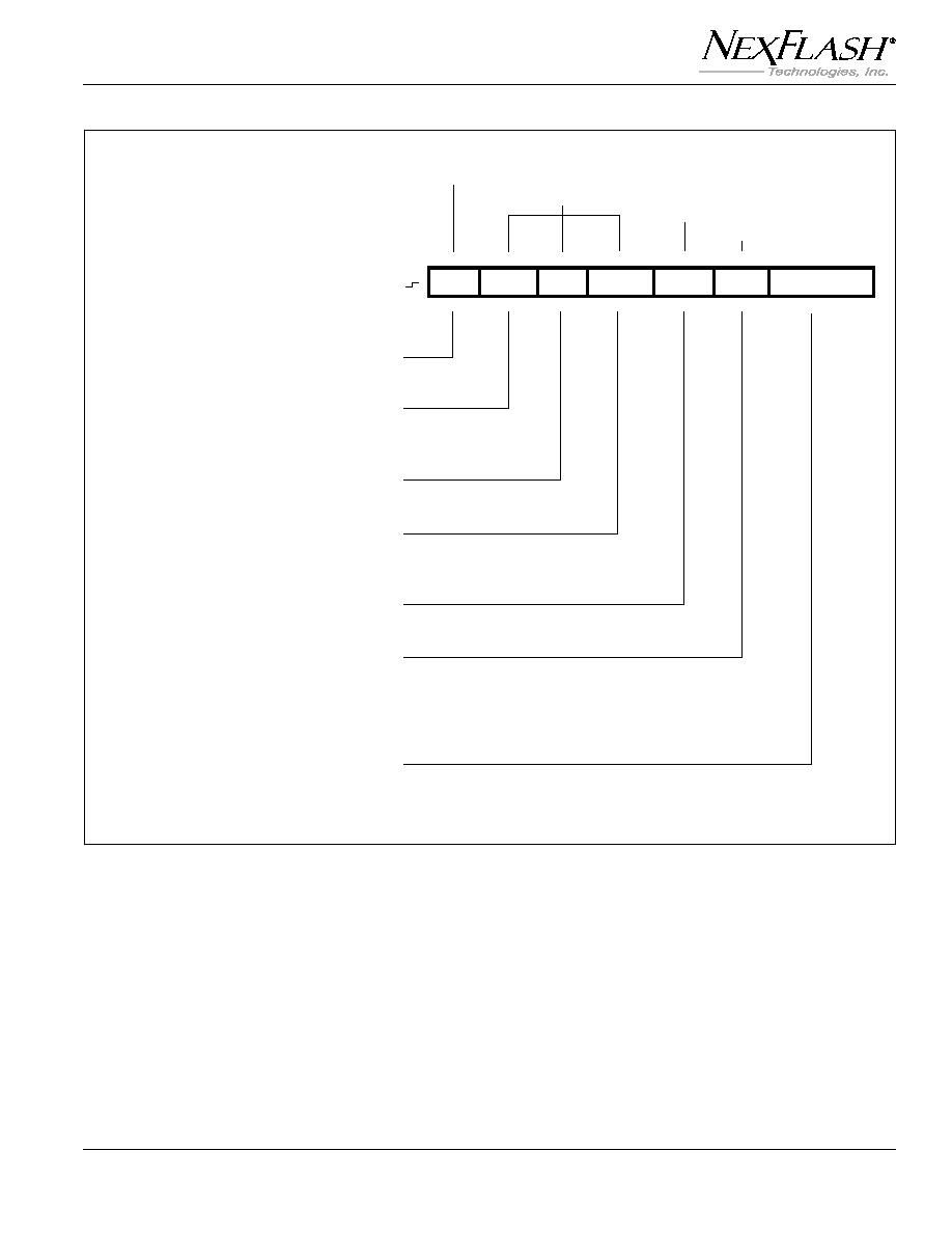
C3-C0 SA11-0 DA3-0 SA15-12 R31-R0 S15-S0 D0 - - - D2112
INITIAL CLOCK
To wake device from standby
(Data is "Don't Care")
COMMAND TYPE
1H = Read
MAIN SECTOR ADDRESS
000H-1FF for NX26F011A
000H-7FF for NX26F041A
DEVICE ADDRESS
A0-A3 pins = 0H-FH
AUXILARY SECTOR ADDRESS
0H = To address main sector address 0-FFF
5H = Device information sector
RESERVED
Use 00 00 00 00H
INPUT STATUS BYTES
9999H = Ready, 6666H = Busy
Note: Delay is required during
status byte read, see
t
RP
in
AC Characteristics
INPUT SECTOR DATA BITS
0-2112 (264 Bytes)
Command
Address
Reserved
Status
Data
Figure 5. Sector Read Instruction - Sequence and Bit Instruction