W24LH8
32K
◊
8 CMOS STATIC RAM
Publication Release Date: March 2001
- 1 - Revision A3
GENERAL DESCRIPTION
The W24LH8 is a normal speed, very low power CMOS static RAM organized as 32768
◊
8 bits that
operates on a wide voltage range from 2.7V to 5.5V power supply. The W24LH8 family, W24LH8-55LE
and W24LH8-55LI, can meet requirement of various operating temperature. This device is
manufactured using Winbond's high performance CMOS technology.
FEATURES
∑
Low power consumption
∑
Access time: 55 nS (5V
±
10%),
100 nS (3V
±
10%)
∑
2.7V to 5.5V supply voltage
∑
Fully static operation
∑
All inputs and outputs directly TTL compatible
∑
Three-state outputs
∑
Battery back-up operation capability
∑
Data retention voltage: 2V (min.)
∑
Available packages: 330 mil SOP and standard
type one TSOP (8 mm
◊
13.4 mm)
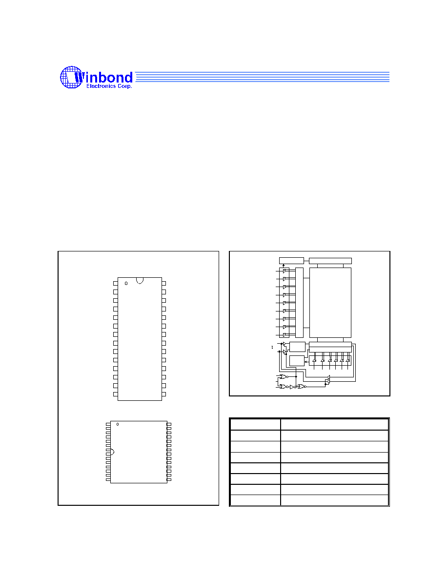
PIN CONFIGURATIONS
1
2
3
4
5
6
7
8
9
10
11
12
13
14
28-pin
SOP
28
27
26
25
24
23
22
21
20
19
18
17
16
15
V
DD
#WE
A13
A8
A9
A11
#OE
A10
#CS
I/O8
I/O7
I/O6
I/O5
I/O4
A14
A12
A7
A6
A5
A4
A3
A2
A1
A0
I/O1
I/O2
I/O3
V
SS
1
2
3
4
5
6
7
8
9
10
11
12
13
14
28
27
26
25
24
23
22
21
20
19
18
17
16
15
28-pin
TSOP
#OE
A11
A9
A8
A13
#WE
V
DD
A14
A12
A7
A6
A5
A4
A3
A10
#CS
I/O8
I/O7
I/O6
I/O5
I/O4
I/O3
I/O2
I/O1
A0
A1
A2
V
SS
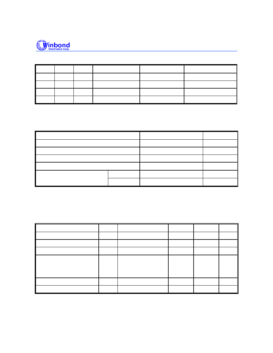
BLOCK DIAGRAM
CLK GEN.
PRECHARGE CKT.
CORE CELL ARRAY
512 ROWS
64 X 8 COLUMNS
DATA
CNTRL.
CLK
GEN.
R
O
W
D
E
C
O
D
E
R
A12
A14
A2
A3
A4
A5
A6
A7
A13
A11
I/O CKT.
COLUMN DECODER
#OE
#WE
#CS
I/O1
I/O8
A10 A1 A0 A8 A9
PIN DESCRIPTION
SYMBOL
DESCRIPTION
A0
-
A14
Address Inputs
I/O1
-
I/O8
Data Inputs/Outputs
#CS
Chip Select Input
#WE
Write Enable Input
#OE
Output Enable Input
V
DD
Power Supply
V
SS
Ground
W24LH8
- 2 -
TRUTH TABLE
#CS
#OE
#WE
MODE
I/O1
-
I/O8
V
DD
CURRENT
H
X
X
Not Selected
High Z
I
SB
, I
SB
1
L
H
H
Output Disable
High Z
I
DD
L
L
H
Read
Data Out
I
DD
L
X
L
Write
Data In
I
DD
DC CHARACTERISTICS
Absolute Maximum Ratings
PARAMETER
RATING
UNIT
Supply Voltage to V
SS
Potential
-0.5 to +7.0
V
Input/Output to V
SS
Potential
-0.5 to V
DD
+0.5
V
Allowable Power Dissipation
1.0
W
Storage Temperature
-65 to +150
∞
C
Operating Temperature
LE
-20 to 85
∞
C
LI
-40 to 85
∞
C
Note: Exposure to conditions beyond those listed under Absolute Maximum Ratings may adversely affect the life and reliability
of the device.
Operating Characteristics
(V
SS
= 0V; T
A
(
∞
C) = -20 to 85 for LE; -40 to 85 for LI)
PARAMETER
SYM.
TEST CONDITIONS
MIN.
MAX.
UNIT
Input Low Voltage
V
IL
-
-0.5
+0.6
V
Input High Voltage
V
IH
-
+2.0
V
DD
+0.5
V
Input Leakage Current
I
LI
V
IN
= V
SS
to V
DD
-1
+1
µ
A
Output Leakage Current
I
LO
V
I/O
= V
SS
to V
DD,
#CS = V
IH
(min.) or
#OE = V
IH
(min.) or
#WE = V
IL
(max.)
-1
+1
µ
A
Output Low Voltage
V
OL
I
OL
= +2.1 mA
-
0.4
V
Output High Voltage
V
OH
I
OH
= -1.0 mA
2.2
-
V
W24LH8
Publication Release Date: March 2001
- 3 - Revision A3
Operating Characteristics, continued
PARAMETER
SYM.
TEST CONDITIONS
MIN. TYP. MAX. UNIT
Operating Power Supply I
DD
#CS = V
IL
(max.), I/O = 0 mA, 5V
-
-
70
mA
Current
Cycle = min. Duty = 100%
3V
-
-
40
Standby Power Supply
Current
I
SB
#CS = V
IH
(min.), Cycle = min.
Duty = 100%
-
-
1
mA
I
SB1
#CS
V
DD
-0.2V
-
0.5
5
µ
A
Note: Typical parameter is measured under ambient temperature T
A
= 25
∞
C and V
DD
= 5V/ 3V.
CAPACITANCE
(T
A
= 25
∞
C, f = 1 MHz)
PARAMETER
SYM.
CONDITIONS
MAX.
UNIT
Input Capacitance
C
IN
V
IN
= 0V
6
pF
Input/Output Capacitance
C
I/O
V
OUT
= 0V
8
pF
Note: These parameters are sampled but not 100% tested.
AC CHARACTERISTICS
AC Test Conditions
PARAMETER
CONDITIONS
Input Pulse Levels
0V to 2.4V
Input Rise and Fall Times
5 nS
Input and Output Timing Reference Level
1.5V
Output Load
See the drawing below
AC Test Loads and Waveform
90%
90%
5 nS
10%
5 nS
10%
OUTPUT
OUTPUT
2.4V
0V
100 pF
Including
Jig and
Scope
5 pF
Including
Jig and
Scope
1 TTL
1 TTL
CLZ,
OLZ,
CHZ
,
OHZ,
WHZ, OW
(For T
T
T
T
T
T
)
W24LH8
- 4 -
AC Characteristics, continued
(V
SS
= 0V; T
A
(
∞
C) = -20 to 85 for LE; -40 to 85 for LI)
Read Cycle
PARAMETER
SYMBOL
3V
±
10%
5V
±
10%
UNIT
MIN.
MAX.
MIN.
MAX.
Read Cycle Time
T
RC
100
-
55
-
nS
Address Access Time
T
AA
-
100
-
55
nS
Chip Select Access Time
T
ACS
-
100
-
55
nS
Output Enable to Output Valid
T
AOE
-
50
-
30
nS
Chip Selection to Output in Low Z
T
CLZ
*
15
-
10
-
nS
Output Enable to Output in Low Z
T
OLZ
*
5
-
5
-
nS
Chip Deselection to Output in High Z
T
CHZ
*
-
35
-
20
nS
Output Disable to Output in High Z
T
OHZ
*
-
35
-
20
nS
Output Hold from Address Change
T
OH
15
-
10
-
nS
These parameters are sampled but not 100% tested
Write Cycle
PARAMETER
SYMBOL
3V
±
10%
5V
±
10%
UNIT
MIN.
MAX.
MIN.
MAX.
Write Cycle Time
T
WC
100
-
55
-
nS
Chip Selection to End of Write
T
CW
80
-
40
-
nS
Address Valid to End of Write
T
AW
80
-
40
-
nS
Address Setup Time
T
AS
0
-
0
-
nS
Write Pulse Width
T
WP
70
-
30
-
nS
Write Recovery Time #CS, #WE
T
WR
0
-
0
-
nS
Data Valid to End of Write
T
DW
40
-
25
-
nS
Data Hold from End of Write
T
DH
0
-
0
-
nS
Write to Output in High Z
T
WHZ
*
-
35
-
20
nS
Output Disable to Output in High Z
T
OHZ
*
-
35
-
20
nS
Output Active from End of Write
T
OW
5
-
5
-
nS
These parameters are sampled but not 100% tested
W24LH8
Publication Release Date: March 2001
- 5 - Revision A3
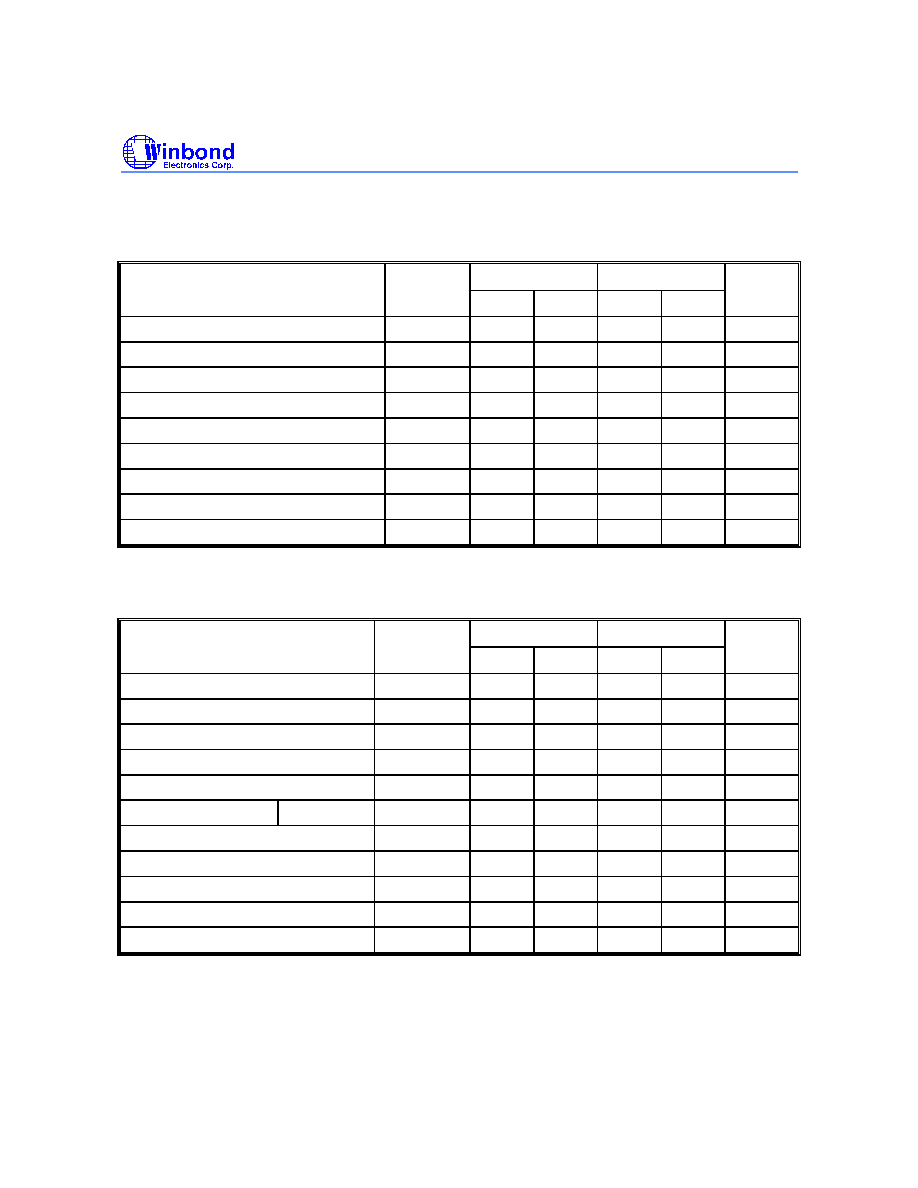
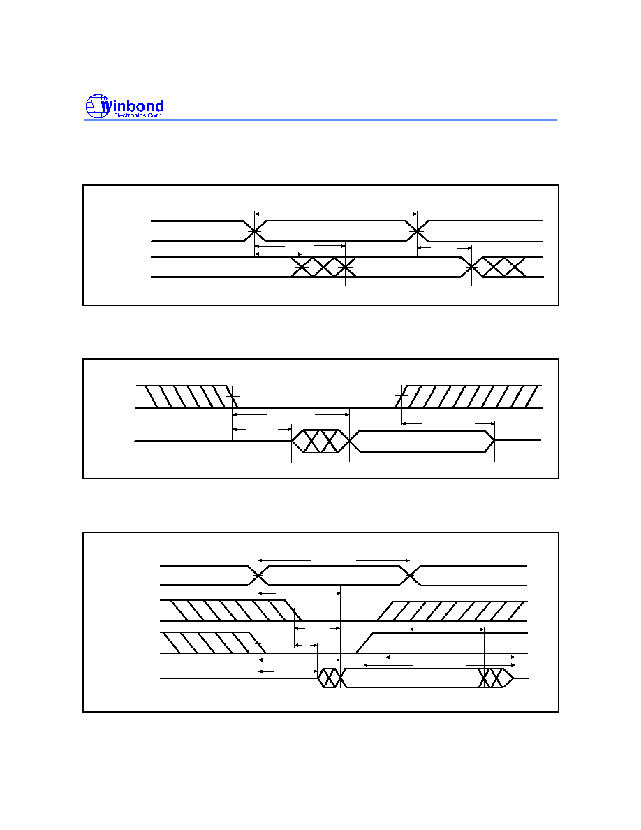
TIMING WAVEFORMS
Read Cycle 1
(Address Controlled)
Address
T
RC
T
AA
T
OH
T
OH
D
OUT
Read Cycle 2
(Chip Select Controlled)
#CS
D
OUT
T
CLZ
T
ACS
CHZ
T
Read Cycle 3
(Output Enable Controlled)
Address
T
RC
#CS
D
OUT
T AA
#OE
T
AOE
T
OLZ
T
OH
CLZ
T
CHZ
T
T
ACS
T
OHZ