Preliminary W25S243A
64K
◊
64 BURST PIPELINED HIGH-SPEED
CMOS STATIC RAM
Publication Release Date: November 1998
- 1 -
Revision A1
GENERAL DESCRIPTION
The W25S243A is a high-speed, low-power, synchronous-burst pipelined, CMOS static RAM
organized as 65,536
◊
64 bits that operates on a single 3.3-volt power supply. A built-in two-bit burst
address counter supports both Pentium
TM
burst mode and linear burst mode. The mode to be
executed is controlled by the LBO pin. Pipelining or non-pipelining of the data outputs is controlled by
the FT pin. A snooze mode can reduces power dissipation.
This device supports 3-1-1-1-2-1-1-1 in a two-bank, back-to-back burst read cycle.
FEATURES
∑
Synchronous operation
∑
High-speed access time: 12 nS
∑
Single +3.3V power supply
∑
Individual byte write capability
∑
3.3V LVTTL compatible I/O
∑
Clock-controlled and registered input
∑
Asynchronous output enable
∑
Pipelined/non-pipelined data output capability
∑
Supports snooze mode (low-power state)
∑
Internal burst counter supports Intel burst
(Interleaved) mode & linear burst mode
∑
Supports 2T/1T mode
∑
Packaged in 128-pin QFP and TQFP
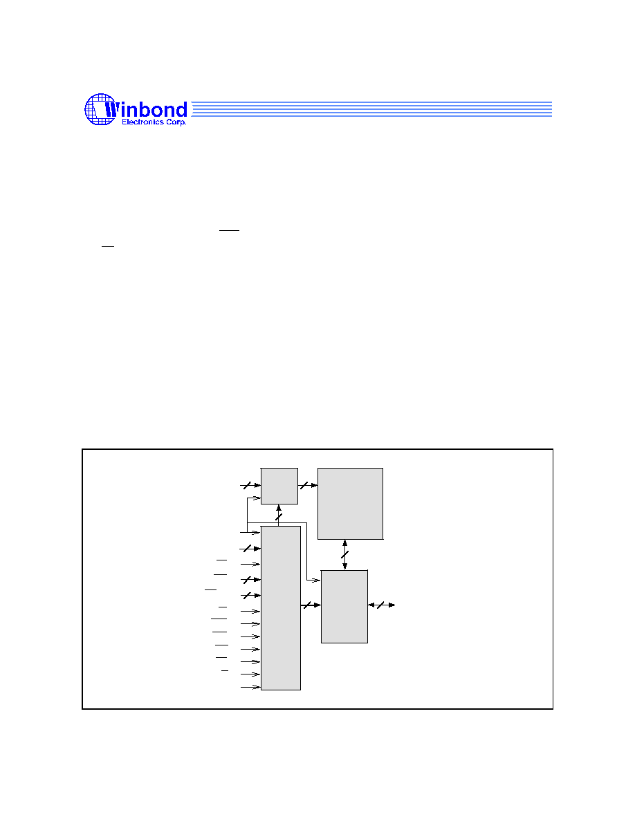
BLOCK DIAGRAM
A(15:0)
DATA I/O
REGISTER
INPUT
REGISTER
CONTROL
LOGIC
REGISTER
64K X 64
CORE
ARRAY
CE(3:1)
BWE
CLK
OE
GW
ADSC
ADSP
ADV
LBO
BW(8:1)
I/O(64:1)
FT
ZZ
Preliminary W25S243A
- 2 -
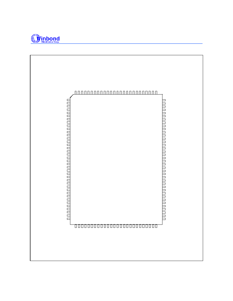
PIN CONFIGURATION
V
S
S
Q
/
F
T
/
L
B
O
A
1
5
A
1
4
A
1
3
V
D
D
V
S
S
A
1
2
A
1
1
A
1
0
A
9
R
S
V
A
8
A
7
A
6
A
5
A
4
A
3
V
D
D
V
S
S
A
2
A
1
A
0
Z
Z
V
D
D
Q
VDDQ
I/O32
I/O31
I/O30
I/O29
I/O28
I/O27
I/O26
I/O25
I/O24
I/O23
I/O22
VSSQ
VDDQ
I/O21
I/O20
I/O19
I/O18
I/O17
I/O16
I/O15
I/O14
I/O13
I/O12
VSSQ
VDDQ
I/O11
I/O10
I/O9
I/O8
I/O7
I/O6
I/O5
I/O4
I/O3
I/O2
I/O1
VSSQ
1
2
3
4
5
6
7
8
9
10
11
12
13
14
15
16
17
18
19
20
21
22
23
24
25
26
27
28
29
30
31
32
33
34
35
36
37
38
102
101
100
99
98
97
96
95
94
93
92
91
90
89
88
87
86
85
84
83
82
81
80
79
78
77
76
75
74
73
72
71
70
69
68
67
66
65
5
2
3
9
4
0
4
1
4
2
4
3
4
4
4
5
4
6
4
7
4
8
4
9
5
0
5
1
5
3
5
4
5
5
5
6
5
7
5
8
5
9
6
0
6
1
6
2
6
3
6
4
V
S
S
Q
V
D
D
Q
C
E
2
/
C
E
3
V
S
S
V
D
D
/
C
E
/
B
W
8
/
B
W
7
/
B
W
6
/
B
W
5
/
O
E
C
L
K
/
B
W
E
/
G
W
/
B
W
4
/
B
W
3
V
S
S
V
D
D
/
B
W
2
/
B
W
1
/
A
D
S
C
/
A
D
S
P
/
A
D
V
1
2
8
1
2
7
1
2
6
1
2
5
1
2
4
1
2
3
1
2
2
1
2
1
1
2
0
1
1
9
1
1
8
1
1
7
1
1
6
1
1
4
1
1
3
1
1
2
1
1
1
1
1
0
1
0
9
1
0
8
1
0
7
1
0
6
1
0
5
1
0
4
1
0
3
1
1
5
VSSQ
I/O33
I/O34
I/O35
I/O36
I/O37
I/O38
I/O39
I/O40
I/O41
I/O42
I/O43
VDDQ
VSSQ
I/O44
I/O45
I/O46
I/O47
I/O48
I/O49
I/O50
I/O51
I/O52
I/O53
VDDQ
VSSQ
I/O54
I/O55
I/O56
I/O57
I/O58
I/O59
I/O60
I/O61
I/O62
I/O63
I/O64
VDDQ
N
C
N
C

Preliminary W25S243A
Publication Release Date: November 1998
- 3 -
Revision A1
PIN DESCRIPTION
SYMBOL
TYPE
DESCRIPTION
A0
-
A15
Input, Synchronous
Host address
I/O1
-
I/O64
I/O, Synchronous
Data Inputs/Outputs
CLK
Input, Clock
Processor host bus clock
CE1, CE2, CE3
Input, Synchronous
Chip enables
GW
Input, Synchronous
Global write
BWE
Input, Synchronous
Byte write enable from cache controller
BW1
-
BW8
Input, Synchronous
Host bus byte enables used with BWE
OE
Input, Asynchronous
Output enable input
ADV
Input, Synchronous
Internal burst address counter advance
ADSC
Input, Synchronous
Address status from Chip Set
ADSP
Input, Synchronous
Address status from CPU
ZZ
Input, Asynchronous
Snooze pin for low-power state, internal pull low
FT
Input, Static
Connected to V
SSQ
: Device operates in flow-
through (non-pipelined) mode
.
Connected to V
DDQ
or unconnected
:
Device
operates in pipelined mode
.
LBO
Input, Static
Lower address burst order
Connected to V
SSQ
: Device is in linear mode.
Connected to V
DDQ
or unconnected: Device is in
non-linear mode.
V
DDQ
I/O power supply
V
SSQ
I/O ground
V
DD
Power supply
V
SS
Ground
RSV
Reserved pin, don't use these pins
NC
No connection
Preliminary W25S243A
- 4 -
FUNCTIONAL DESCRIPTION
The W25S243A is a synchronous-burst pipelined SRAM designed for use in high-end personal
computers. It supports two burst address sequences for Intel
TM
systems (Interleaved mode) and linear
mode, which can be controlled by the
LBO
pin. The burst cycles are initiated by ADSP or ADSC
and the burst counter is incremented whenever ADV is sampled low. The device can also be
switched to non-pipelined mode if necessary.
BURST ADDRESS SEQUENCE
INTEL SYSTEM ( LBO = V
DDQ
)
LINEAR MODE ( LBO = V
SSQ
)
A[1:0]
A[1:0]
A[1:0]
A[1:0]
A[1:0]
A[1:0]
A[1:0]
A[1:0]
External Start Address
00
01
10
11
00
01
10
11
Second Address
01
00
11
10
01
10
11
00
Third Address
10
11
00
01
10
11
00
01
Fourth Address
11
10
01
00
11
00
01
10
The device supports several types of write mode operations. BWE and BW [8:1] support individual
byte writes. The BE [7:0] signals can be directly connected to the SRAM BW [8:1]. The GW signal is
used to override the byte enable signals and allows the cache controller to write all bytes to the
SRAM, no matter what the byte write enable signals are. The various write modes are indicated in the
Write Table below. Note that in pipelined mode, the byte write enable signals are not latched by the
SRAM with addresses but with data. In pipelined mode, the cache controller must ensure the SRAM
latches both data and valid byte enable signals from the processor.
TRUTH TABLE
CYCLE
ADDRESS
USED
CE1
CE2
CE3
ADSP
ADSC
ADV
OE
DATA
WRITE*
Unselected
No
1
X
X
X
0
X
X
Hi-Z
X
Unselected
No
0
X
1
0
X
X
X
Hi-Z
X
Unselected
No
0
0
X
0
X
X
X
Hi-Z
X
Unselected
No
0
X
1
1
0
X
X
Hi-Z
X
Unselected
No
0
0
X
1
0
X
X
Hi-Z
X
Begin Read
External
0
1
0
0
X
X
X
Hi-Z
X
Begin Read
External
0
1
0
1
0
X
X
Hi-Z
Read
Continue Read
Next
X
X
X
1
1
0
1
Hi-Z
Read
Continue Read
Next
X
X
X
1
1
0
0
D-Out
Read
Continue Read
Next
1
X
X
X
1
0
1
Hi-Z
Read
Continue Read
Next
1
X
X
X
1
0
0
D-Out
Read
Suspend Read
Current
X
X
X
1
1
1
1
Hi-Z
Read
Suspend Read
Current
X
X
X
1
1
1
0
D-Out
Read
Suspend Read
Current
1
X
X
X
1
1
1
Hi-Z
Read
Suspend Read
Current
1
X
X
X
1
1
0
D-Out
Read

Preliminary W25S243A
Publication Release Date: November 1998
- 5 -
Revision A1
Truth Table, continued
CYCLE
ADDRESS
USED
CE1
CE2
CE3
ADSP
ADSC
ADV
OE
DATA
WRITE*
Begin Write
Current
X
X
X
1
1
1
X
Hi-Z
Write
Begin Write
Current
1
X
X
X
1
1
X
Hi-Z
Write
Begin Write
External
0
1
0
1
0
X
X
Hi-Z
Write
Continue Write
Next
X
X
X
1
1
0
X
Hi-Z
Write
Continue Write
Next
1
X
X
X
1
0
X
Hi-Z
Write
Suspend Write
Current
X
X
X
1
1
1
X
Hi-Z
Write
Suspend Write
Current
1
X
X
X
1
1
X
Hi-Z
Write
Notes:
1. For a detailed definition of read/write, see the Write Table below.
2. An "X" means don't care, "1" means logic high, and "0" means logic low.
3. The OE pin enables the data output but is not synchronous with the clock. All signals of the SRAM are sampled synchronous to
the bus clock except for the OE pin.
4. On a write cycle that follows a read cycle, OE must be inactive prior to the start of write cycle to allow write data to setup
the SRAM. OE must also disable the output buffer prior to the finish of a write cycle to ensure the SRAM data hold timings are
met.
WRITE TABLE
READ/WRITE FUNCTION
GW
BWE
BW8
BW7
BW6
BW5
BW4
BW3
BW2
BW1
Read
1
1
X
X
X
X
X
X
X
X
Read
1
0
1
1
1
1
1
1
1
1
Write byte 1 I/O1
-
I/O8
1
0
1
1
1
1
1
1
1
0
Write byte 2 I/O9
-
I/O16
1
0
1
1
1
1
1
1
0
1
Write byte 2, byte 1
1
0
1
1
1
1
1
1
0
0
Write byte 3 I/O17
-
I/O24
1
0
1
1
1
1
1
0
1
1
Write byte 3, byte 1
1
0
1
1
1
1
1
0
1
0
Write byte 3, byte 2
1
0
1
1
1
1
1
0
0
1
Write byte 3, byte 2, byte 1
1
0
1
1
1
1
1
0
0
0
Write byte 4, I/O25
-
I/O32
1
0
1
1
1
1
0
1
1
1
Write byte 4, byte 1
1
0
1
1
1
1
0
1
1
0
Write byte 4, byte 2
1
0
1
1
1
1
0
1
0
1
Write byte 4, byte 2, byte 1
1
0
1
1
1
1
0
1
0
0
Write byte 4, byte 3
1
0
1
1
1
1
0
0
1
1
Write byte 4, byte 3, byte 1
1
0
1
1
1
1
0
0
1
0
Write byte 4, byte 3, byte 2
1
0
1
1
1
1
0
0
0
1
Write byte 4, byte 3, byte 2, byte 1
1
0
1
1
1
1
0
0
0
0
Write byte 5, I/O33
-
I/O40
1
0
1
1
1
0
1
1
1
1
Write byte 5, byte 1
1
0
1
1
1
0
1
1
1
0

Preliminary W25S243A
- 6 -
Write Table, continued
READ/WRITE FUNCTION
GW
BWE
BW8
BW7
BW6
BW5
BW4
BW3
BW2
BW1
Write byte 5, byte 2
1
0
1
1
1
0
1
1
0
1
Write byte 5, byte 2, byte 1
1
0
1
1
1
0
1
1
0
0
Write byte 5, byte 3
1
0
1
1
1
0
1
0
1
1
Write byte 5, byte 3, byte 1
1
0
1
1
1
0
1
0
1
0
Write byte 5, byte 3, byte 2
1
0
1
1
1
0
1
0
0
1
Write byte 5, byte 3, byte 2, byte 1
1
0
1
1
1
0
1
0
0
0
Write byte 5, byte 4
1
0
1
1
1
0
0
1
1
1
Write byte 5, byte 4, byte 1
1
0
1
1
1
0
0
1
1
0
Write byte 5, byte 4, byte 2
1
0
1
1
1
0
0
1
0
1
Write byte 5, byte 4, byte 2, byte 1
1
0
1
1
1
0
0
1
0
0
Write byte 5, byte 4, byte 3
1
0
1
1
1
0
0
0
1
1
Write byte 5, byte 4, byte 3, byte 1
1
0
1
1
1
0
0
0
1
0
Write byte 5, byte 4, byte 3, byte 2
1
0
1
1
1
0
0
0
0
1
Write byte 5, byte 4, byte 3, byte 2,
byte 1
1
0
1
1
1
0
0
0
0
0
Write byte 6
1
0
1
1
0
1
1
1
1
1
Write byte 6, byte 1
1
0
1
1
0
1
1
1
1
0
Write byte 6, byte 2
1
0
1
1
0
1
1
1
0
1
Write byte 6, byte 2, byte 1
1
0
1
1
0
1
1
1
0
0
..... and so on .....
...
...
...
...
...
...
...
...
...
...
Write byte 8, byte 7, byte 6, byte 5,
byte 4, byte 2, byte 1
1
0
0
0
0
0
0
1
0
0
Write byte 8, byte 7, byte 6, byte 5,
byte 4, byte 3
1
0
0
0
0
0
0
0
1
1
Write byte 8, byte 7, byte 6, byte 5,
byte 4, byte 3, byte 1
1
0
0
0
0
0
0
0
1
0
Write byte 8, byte 7, byte 6, byte 5,
byte 4, byte 3, byte 2
1
0
0
0
0
0
0
0
0
1
Write all bytes
1
0
0
0
0
0
0
0
0
0
Write all bytes
0
x
x
x
x
x
x
x
x
x
The ZZ state is a low-power state in which the device consumes less power than in the unselected
mode. Enabling the ZZ pin for a fixed period of time will force the SRAM into the ZZ state. Pulling the
ZZ pin low for a set period of time will wake up the SRAM again. While the SRAM is in ZZ mode, data
retention is guaranteed, but the chip will not monitor any input signal except for the ZZ pin. In the
unselected mode, on the other hand, all the input signals are monitored.

Preliminary W25S243A
Publication Release Date: November 1998
- 7 -
Revision A1
DC CHARACTERISTICS
Absolute Maximum Ratings
PARAMETER
RATING
UNIT
Core Supply Voltage to Vss
-0.5 to 4.6
V
I/O Supply Voltage to Vss
-0.5 to 4.6
V
Input/Output to V
SSQ
Potential
V
SSQ
-0.5 to V
DDQ
+0.5
V
Allowable Power Dissipation
1.0
W
Storage Temperature
-65 to 150
∞
C
Operating Temperature
0 to +70
∞
C
Note: Exposure to conditions beyond those listed under Absolute Maximum Ratings may adversely affect the life and reliability of the
device.
Operating Characteristics
(V
DD
/V
DDQ
= 3.15V to 3.6V, V
SS
/V
SSQ
= 0V, T
A
= 0 to 70
∞
C)
PARAMETER
SYM.
TEST CONDITIONS
MIN.
TYP.
MAX.
UNIT
Input Low Voltage
V
IL
-
-0.5
-
+0.8
V
Input High Voltage
V
IH
-
+2.0
-
V
DD
+0.3
V
Input Leakage Current
I
LI
V
IN
= V
SSQ
to V
DDQ
-10
-
+10
µ
A
Output Leakage
Current
I
LO
V
I/O
= V
SSQ
to V
DDQ,
and data
I/O pins in high-Z state defined
in truth table
-10
-
+ 10
µ
A
Output Low Voltage
V
OL
I
OL
= +8.0 mA
-
-
0.4
V
Output High Voltage
V
OH
I
OH
= -4.0 mA
2.4
-
-
V
Operating Current
I
DD
T
CYC
min. , I/O = 0 mA
-
-
350
mA
Standby Current
I
SB
Unselected mode defined in
truth table, V
IN
, V
IO
= V
IH
(min.)
/V
IL
(max.) T
CYC
min.
-
-
80
mA
ZZ Mode Current
I
ZZ
ZZ mode, T
CYC
min.
-
-
5
mA
Note: Typical characteristics are measured at V
DD
= 3.3V, T
A
= 25
∞
C.
CAPACITANCE
(V
DD
= 3.3V, T
A
= 25
∞
C, f = 1 MHz)
PARAMETER
SYM.
CONDITIONS
MAX.
UNIT
Input Capacitance
C
IN
V
IN
= 0V
6
pF
Input/Output Capacitance
C
I/O
V
OUT
= 0V
8
pF
Note: These parameters are sampled but not 100% tested.

Preliminary W25S243A
- 8 -
AC CHARACTERISTICS
AC Test Conditions
PARAMETER
CONDITIONS
Input Pulse Levels
0V to 3V
Input Rise and Fall Times
2 nS
Input and Output Timing Reference Level
1.5V
Output Load
C
L
= 30 pF, I
OH
/I
OL
= -4 mA/8 mA
AC Test Loads and Waveform
90%
90%
2 nS
10%
2 nS
10%
RL = 50 ohm
VL = 1.5V
OUTPUT
5 pF
R2
350 ohm
R1 320 ohm
3.3V
OUTPUT
30 pF
Including
Jig and
Scope
3.0V
0V
Including
Jig and
Scope
Zo = 50 ohm
(For T
KHZ,
T
KLZ,
T
OHZ,
T
OLZ,
measurement)
AC Timing Characteristics
(V
DD
/V
DDQ
= 3.15V to 3.6V, V
SS
/V
SSQ
= 0V, T
A
= 0 to 70
∞
C, all timings measured in pipelined mode)
PARAMETER
SYMBOL
W25S243A-12
UNIT
NOTES
MIN.
MAX.
Add. Setup Time
T
AS
2.5
-
nS
Add. Hold Time
T
AH
0.5
-
nS
Write Data Setup Time
T
DS
2.5
-
nS
Write Data Hold Time
T
DH
0.5
-
nS
ADV
Setup Time
T
ADVS
2.5
-
nS
ADV
Hold Time
T
ADVH
0.5
-
nS
Preliminary W25S243A
Publication Release Date: November 1998
- 9 -
Revision A1
AC Timing Characteristics, continued
PARAMETER
SYMBOL
W25S243A-12
UNIT
NOTES
MIN.
MAX.
ADSP
Setup Time
T
ADSS
2.5
-
nS
ADSP
Hold Time
T
ADSH
0.5
-
nS
ADSC
Setup Time
T
ADCS
2.5
-
nS
ADSC
Hold Time
T
ADCH
0.5
-
nS
CE1
, CE2,
CE3
Setup Time
T
CES
2.5
-
nS
CE1
, CE2,
CE3
Hold Time
T
CEH
0.5
-
nS
GW
,
BWE
X Setup Time
T
WS
2.5
-
nS
GW
,
BWE
X Hold Time
T
WH
0.5
-
nS
Clock Cycle Time
T
CYC
15
-
nS
Clock High Pulse Width
T
KO
6
-
nS
Clock Low Pulse Width
T
KL
6
-
nS
Clock to Output Valid
T
KQ
-
12
nS
Clock to Output High-Z
T
KHZ
2
15
nS
1
Clock to Output Low-Z
T
KLZ
0
-
nS
1
Clock to Output Invalid
T
KX
2
-
nS
1
Output Enable to Output
Valid
T
OE
-
7
nS
Output Enable to Output
High-Z
T
OHZ
-
7
nS
1
Output Enable to Output
Low-Z
T
OLZ
0
-
nS
1
Output Enable to Output
Invalid
T
OX
0
-
nS
ZZ Standby Time
T
ZZS
-
100
nS
2
ZZ Recover Time
T
ZZR
100
-
nS
3
Notes:
1. These parameters are sampled but not 100% tested
2. In the ZZ mode, the SRAM will enter a low-power state. In this mode, data retention is guaranteed and the clock is active.
3. ADSC and ADSP should not be accessed for at least 100 nS after chip leaves ZZ mode.
4. Configuration signals LBO and FT are static and should not be changed during operation.

Preliminary W25S243A
- 10 -
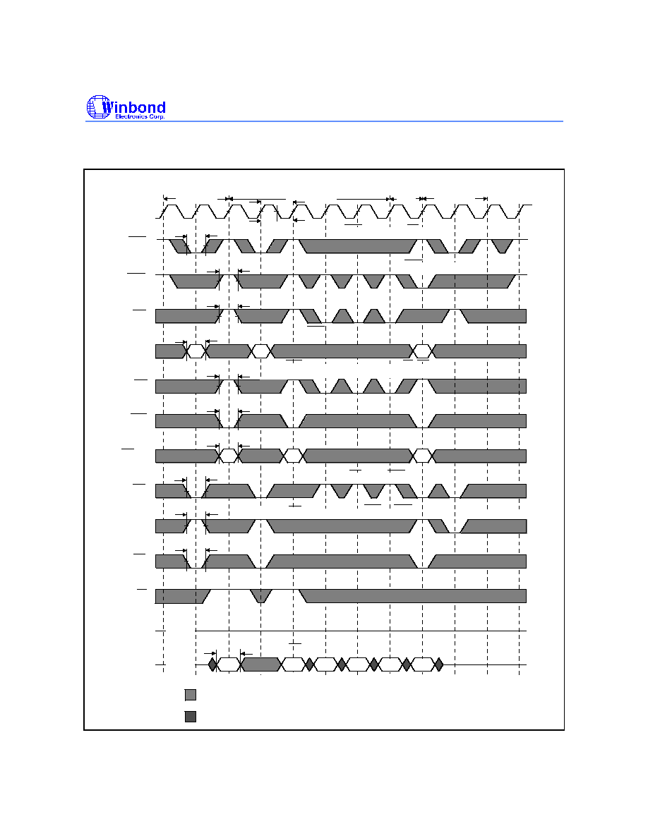
TIMING WAVEFORMS
Read Cycle Timing
Single Read
Burst Read
Unselected
T
CYC
CLK
T
ADSS
T
ADSH
T
KH
T
KL
ADSP is blocked by CE1 inactive
T
ADCS
T
ADCH
ADSC initiated read
T
ADVS
T
ADVH
T
AS
T
AH
RD1
RD2
RD3
T
WS
T
WH
T
WS
T
WH
T
CES
T
CEH
CE1 masks ADSP
T
CES
T
CEH
T
CES
T
CEH
CE2 and CE3 only sampled with ADSP or ADSC
Unselected with CE2
T
OE
T
OHZ
ADSP
ADSC
ADV
A[15:0]
GW
BWE
BW[4:1]
CE1
CE2
CE3
Suspend Burst
DON'T CARE
UNDEFINED
3a
2d
2c
2b
2a
1a
T
OLZ
T
OX
T
KX
T
KHZ
T
KX
High-Z
High-Z
OE
Data-Out
Data-In
T
KLZ
T
KQ
Preliminary W25S243A
Publication Release Date: November 1998
- 11 -
Revision A1
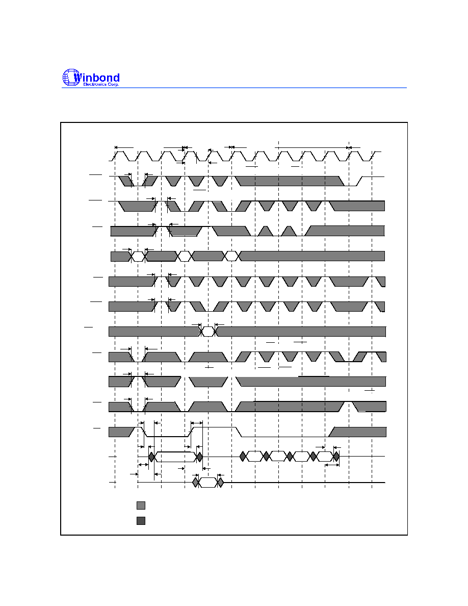
Timing Waveforms, continued
Write Cycle Timing
1a
Single Write
Burst Write
Unselected
T
CYC
CLK
T
ADSS
T
ADSH
T
KH
T
KL
ADSP is blocked by CE1 inactive
T
ADCS
T
ADCH
ADSC initiated write
T
ADVS
T
ADVH
T
AS
T
AH
WR1
WR2
WR3
T
WS
T
WH
T
WS
T
WH
T
CES
T
CEH
CE1 masks ADSP
T
CES
T
CEH
T
CES
T
CEH
CE2 and CE3 only sampled with ADSP or ADSC
Unselected with CE2
High-Z
High-Z
ADSP
ADSC
ADV
A[15:0]
GW
BWE
BW[4:1]
CE1
CE2
CE3
OE
Data-Out
Data-In
2a
2b
2c
2d
3a
Write
GWE allows processor address (and BE=BW)
to be pipelined during a writeback
T
WS
T
WH
WR1
WR2
WR3
T
DS
T
DH
BW[4:1] are applied only to first cycle of WR2
ADV must be inactive for ADSP write
DON'T CARE
UNDEFINED
Preliminary W25S243A
- 12 -
Timing Waveforms, continued
Read/Write Cycle Timing
1a
Single Read
Burst Read
Unselected
T
CYC
CLK
T
ADSS
T
ADSH
T
KH
T
KL
ADSP is blocked by CE1 inactive
ADSC initiated read
T
ADVS
T
ADVH
Suspend Burst
T
AS
T
AH
RD1
T
WS
T
WH
T
WS
T
WH
T
CES
T
CEH
T
CES
T
CEH
T
CES
T
CEH
T
OHZ
T
OH
High-Z
ADSP
ADSC
ADV
A[15:0]
GW
BWE
BW[4:1]
CE1
CE2
CE3
Data-In
Single Write
WR1
RD2
CE1 masks ADSP
CE2 and CE3 only sampled with ADSP or ADSC
Unselected with CE3
T
KHZ
DON'T CARE
UNDEFINED
T
ADCS
T
ADCH
WR1
T
WS
T
WH
T
OE
T
OLZ
High-Z
OE
Data-Out
T
KLZ
T
KQ
1a
T
DS
T
DH
2d
2c
2a
T
KHZ
T
KX
2b

Preliminary W25S243A
Publication Release Date: November 1998
- 13 -
Revision A1
Timing Waveforms, continued
ZZ and RD Timing
1a
Single Read
Snooze -with Data Retention
Read
T
CYC
CLK
T
ADSS
T
ADSH
T
KH
T
KL
T
ADVS
T
ADVH
T
AS
T
AH
RD1
T
WS
T
WH
T
WS
T
WH
T
CES
T
CEH
T
CES
T
CEH
T
CES
T
CEH
T
OHZ
T
OH
High-Z
High-Z
ADSP
ADSC
ADV
A[15:0]
GW
BWE
BW[4:1]
CE1
CE2
CE3
OE
Data-Out
Data-In
RD2
T
KHZ
T
WS
T
WH
RD
RD
T
KX
RD
T
ZZS
T
ZZR
ZZ
DON'T CARE
UNDEFINED
T
OE
T
OLZ
T
KLZ
T
KQ

Preliminary W25S243A
- 14 -
ORDERING INFORMATION
PART NO.
ACCESS
TIME (nS)
OPERATING
CURRENT
MAX. (mA)
STANDBY
CURRENT
MAX. (mA)
PACKAGE
W25S243AF-12
12
350
80
128-pin QFP
W25S243AD-12
12
350
80
128-pin TQFP
Notes
1. Winbond reserves the right to make changes to its products without prior notice.
2. Purchasers are responsible for performing appropriate quality assurance testing on products intended for use in applications
where personal injury might occur as a consequence of product failure.

Preliminary W25S243A
Publication Release Date: November 1998
- 15 -
Revision A1
PACKAGE DIMENSIONS
128-pin QFP
103
128
102
65
64
39
38
1
c
Detail F
See Detail F
1
L
L
Seating Plane
1
A
A
y
E
H
E
b
e
D
D
H
A
2
0.10
0
12
0
0.004
1.60
1.00
17.40
0.80
17.20
0.60
17.00
0.063
0.039
0.685
0.031
0.677
0.023
0.669
0.50
14.10
0.25
0.25
2.87
3.40
14.00
2.72
13.90
0.10
0.15
2.57
0.10
0.555
0.010
0.010
0.113
0.134
0.551
0.107
0.020
0.547
0.004
0.006
0.101
0.004
Symbol
Min.
Nom.
Max.
Max.
Nom.
Min.
Dimension in inches
Dimension in mm
A
b
c
D
e
H
D
H
E
L
y
A
A
L
1
1
2
E
0.008
0.006
0.15
0.20
12
0.783
0.787
0.791
19.90
20.00
20.10
0.905
0.913
0.921
23.00
23.20
23.40
0.055
0.071
1.40
1.80

Preliminary W25S243A
- 16 -
Package Dimensions, continued
128-pin TQFP
103
128
102
65
64
39
38
1
c
Detail F
See Detail F
1
L
L
Seating Plane
1
A
A
y
E
H
E
b
e
D
D
H
A
2
0.10
0
12
0
0.004
1.00
0.75
16.10
0.60
16.00
0.45
15.90
0.039
0.030
0.634
0.024
0.630
0.018
0.626
0.50
14.10
0.25
0.27
1.45
1.60
14.00
1.40
13.90
0.10
0.15
1.35
0.05
0.555
0.010
0.011
0.057
0.063
0.551
0.055
0.020
0.547
0.004
0.006
0.053
0.002
Symbol
Min.
Nom.
Max.
Max.
Nom.
Min.
Dimension in inches
Dimension in mm
A
b
c
D
e
H
D
H
E
L
y
A
A
L
1
1
2
E
0.008
0.006
0.15
0.20
12
0.783
0.787
0.791
19.90
20.00
20.10
0.862
0.866
0.870
21.90
22.00
22.10

Preliminary W25S243A
Publication Release Date: November 1998
- 17 -
Revision A1
VERSION HISTORY
VERSION
DATE
PAGE
DESCRIPTION
A1
Nov. 1998
Initial Issued
Headquarters
No. 4, Creation Rd. III,
Science-Based Industrial Park,
Hsinchu, Taiwan
TEL: 886-3-5770066
FAX: 886-3-5796096
http://www.winbond.com.tw/
Voice & Fax-on-demand: 886-2-27197006
Taipei Office
11F, No. 115, Sec. 3, Min-Sheng East Rd.,
Taipei, Taiwan
TEL: 886-2-27190505
FAX: 886-2-27197502
Winbond Electronics (H.K.) Ltd.
Rm. 803, World Trade Square, Tower II,
123 Hoi Bun Rd., Kwun Tong,
Kowloon, Hong Kong
TEL: 852-27513100
FAX: 852-27552064
Winbond Electronics North America Corp.
Winbond Memory Lab.
Winbond Microelectronics Corp.
Winbond Systems Lab.
2727 N. First Street, San Jose,
CA 95134, U.S.A.
TEL: 408-9436666
FAX: 408-5441798
Note: All data and specifications are subject to change without notice.