W26010A
64K
◊
16 HIGH-SPEED CMOS STATIC RAM
Publication Release Date: May 2001
- 1 - Revision A5
GENERAL DESCRIPTION
The W26010A is a high-speed, low-power CMOS static RAM organized as 65,536
◊
16 bits that
operates on a single 5-volt power supply. This device is manufactured using Winbond's high
performance CMOS technology.
The W26010A has an active low chip select, separate upper and lower byte selects, and a fast output
enable. No clock or refreshing is required. Separate byte select controls (#LB and #UB) allow individual
bytes to be written and read. #LB controls I/O1-I/O8, the lower byte. #UB controls I/O9
-
I/O16, the
upper byte. This device is well suited for use in high-density, high-speed system applications.
FEATURES
∑
High speed access time: 15/20/25 nS (max.)
∑
Low power consumption:
-
Active: 1.3W (max.)
∑
Single
+
5V power supply
∑
Fully static operation
-
No clock or refreshing
∑
All inputs and outputs directly TTL compatible
∑
Three-state outputs
∑
Data byte control
-
#LB (I/O1
-
I/O8), #UB (I/O9
-
I/O16)
∑
Available packages: 44-pin 400 mil SOJ and
Type II TSOP
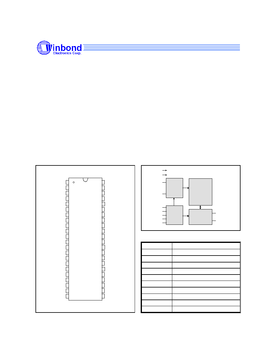
PIN CONFIGURATION
1
2
3
4
5
6
7
8
9
10
11
12
13
14
15
16
17
18
19
20
21
22
44
43
42
41
40
39
38
37
36
35
34
33
32
31
30
29
28
27
26
25
24
23
A0
A1
A2
A3
A4
#CS
I/O1
I/O2
I/O3
I/O4
V
DD
V
SS
I/O5
I/O6
I/O7
I/O8
#WE
A5
A6
A7
A8
NC
NC
A9
A10
A11
A12
NC
I/O9
I/O10
I/O11
I/O12
V
DD
V
SS
I/O13
I/O14
I/O15
I/O16
#LB
#UB
#OE
A13
A14
A15
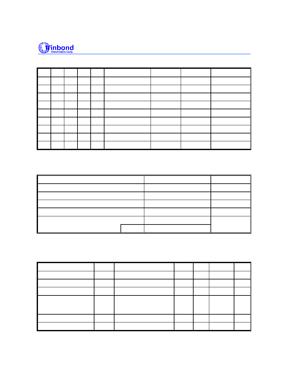
BLOCK DIAGRAM
A0
.
.
A15
I/O1
I/O16
V
DD
V
SS
.
.
DATA I/O
DECODER
CONTROL
#UB
#CS
#OE
#WE
#LB
CORE
ARRAY
PIN DESCRIPTION
SYMBOL
DESCRIPTION
A0
-
A15
Address Inputs
I/O1
-
I/O16 Data Inputs/Outputs
#CS
Chip Select Inputs
#WE
Write Enable Input
#OE
Output Enable Input
#LB
Lower Byte Select I/O1
-
I/O8
#UB
Upper Byte Select I/O9
-
I/O16
V
DD
Power Supply
V
SS
Ground
NC
No Connection
W26010A
- 2 -
TRUTH TABLE
#CS #OE #WE #LB #UB
MODE
I/O1
-
I/O8 I/O9
-
I/O16 V
DD
CURRENT
H
X
X
X
X Not Selected
High Z
High Z
I
SB
, I
SB1
L
H
H
X
X Output Disable
High Z
High Z
I
DD
L
L
H
L
L 2 Bytes Read
D
OUT
D
OUT
I
DD
L
L
H
L
H Lower Byte Read
D
OUT
High Z
I
DD
L
L
H
H
L Upper Byte Read
High Z
D
OUT
I
DD
L
X
L
L
L 2 Bytes Write
D
IN
D
IN
I
DD
L
X
L
L
H Lower Byte Write
D
IN
High Z
I
DD
L
X
L
H
L Upper Byte Write
High Z
D
IN
I
DD
L
X
X
H
H Output Disable
High Z
High Z
I
DD
DC CHARACTERISTICS
Absolute Maximum Ratings
PARAMETER
RATING
UNIT
Supply Voltage to V
SS
Potential
-0.5 to +7.0
V
Input/Output to V
SS
Potential
-0.5 to V
DD
+0.5
V
Allowable Power Dissipation
1.5
W
Storage Temperature
-65 to +150
∞
C
Operating Temperature
0 to +70
∞
C
I
-40 to 85
Note: Exposure to conditions beyond those listed under Absolute Maximum Ratings may adversely affect the life and reliability
of the device.
Operating Characteristics
(V
DD
= 5V
±
10%, V
SS
= 0V, T
A
= 0 to 70
∞
C, I for ≠40 to 85
∞
C)
PARAMETER
SYM.
TEST CONDITIONS
MIN. TYP.
MAX.
UNIT
Input Low Voltage
V
IL
-
-0.5
-
+0.8
V
Input High Voltage
V
IH
-
+2.2
-
V
DD
+0.5
V
Input Leakage Current
I
LI
V
IN
= V
SS
to V
DD
-10
-
+10
µ
A
Output Leakage Current I
LO
V
I/O
= V
SS
to V
DD
Output Pins in High Z
See Truth Table
-10
-
+10
µ
A
Output Low Voltage
V
OL
I
OL
= +8.0 mA
-
-
0.4
V
Output High Voltage
V
OH
I
OH
= -4.0 mA
2.4
-
-
V

W26010A
Publication Release Date: May 2001
- 3 - Revision A5
Operating Characteristics, continued
PARAMETER
SYM.
TEST CONDITIONS
MIN. TYP.
MAX. UNIT
Operating Power
I
DD
#CS = V
IL
(max.),
15
-
-
260
Supply Current
I/O = open, Cycle = min.
20
-
-
220
mA
Duty = 100%
25
-
-
200
Standby Power
Supply Current
I
SB
#CS = V
IH
(min.),
I/O = open
All other pins = V
DD
-0.2V/GND
-
-
50
mA
I
SB1
#CS = V
DD
-0.2V, I/O = open
All other pins = V
DD
-0.2V/GND
-
-
10
mA
Note: Typical characteristics are evaluated at V
DD
= 5V, T
A
= 25
∞
C.
CAPACITANCE
(V
DD
= 5V, T
A
= 25
∞
C, f = 1 MHz)
PARAMETER
SYM.
CONDITIONS
MAX.
UNIT
Input Capacitance
C
IN
V
IN
= 0V
6
pF
Input/Output Capacitance
C
I/O
V
OUT
= 0V
8
pF
Note: These parameters are sampled but not 100% tested.
AC CHARACTERISTICS
AC Test Conditions
PARAMETER
CONDITIONS
Input Pulse Levels
0V to 3V
Input Rise and Fall Times
3 nS
Input and Output Timing Reference Level
1.5V
Output Load
C
L
= 30 pF, I
OH
/I
OL
= -4 mA/8 mA

W26010A
- 4 -
AC Test Loads and Waveform
R1 480 ohm
5V
OUTPUT
R2
255 ohm
5 pF
R2
255 ohm
R1 480 ohm
5V
OUTPUT
30 pF
Including
Jig and
Scope
90%
90%
3 nS
10%
3 nS
10%
3.0V
0V
Including
Jig and
Scope
)
(For T
T
T
OLZ,
T
T
WHZ,
T
OW
T
CLZ, BLZ,
CHZ,
BHZ,
T
OHZ,
(V
DD
= 5V
±
10%, V
SS
= 0V, T
A
= 0 to 70
∞
C,
I
for ≠40 to 85
∞
C)
Read Cycle
PARAMETER
SYM.
W26010A-15 W26010A-20 W26010A-25
UNIT
MIN. MAX. MIN. MAX. MIN. MAX.
Read Cycle Time
T
RC
15
-
20
-
25
-
nS
Address Access Time
T
AA
-
15
-
20
-
25
nS
Chip Select Access Time
T
ACS
-
15
-
20
-
25
nS
Output Enable to Output Valid
TAOE
-
7
-
10
-
12
nS
#UB, #LB Access Time
T
BA
-
7
-
10
-
12
nS
Output Hold from Address Change
T
OH
3
-
3
-
3
-
nS
Chip Select to Output in Low Z
T
CLZ*
3
-
3
-
3
-
nS
Chip Deselect to Output in High Z
T
CHZ*
-
7
-
10
-
12
nS
Output Enable to Output in Low Z
T
OLZ*
0
-
0
-
0
-
nS
Output Disable to Output in High Z
T
OHZ*
-
7
-
10
-
12
nS
#UB, #LB Select to Output in Low Z
T
BLZ*
0
-
0
-
0
-
nS
#UB, #LB Deselect to Output in High Z T
BHZ*
-
7
-
10
-
12
nS
These parameters are sampled but not 100% tested.
W26010A
Publication Release Date: May 2001
- 5 - Revision A5
AC Characteristics, continued
Write Cycle
PARAMETER
SYM. W26010A-15 W26010A-20 W26010A-25 UNIT
MIN. MAX. MIN. MAX. MIN. MAX.
Write Cycle Time
T
WC
15
-
20
-
25
-
nS
Chip Select to End of Write
T
CW
13
-
17
-
18
-
nS
Address Valid to End of Write
T
AW
13
-
17
-
18
-
nS
Address Setup Time
T
AS
0
-
0
-
0
-
nS
#UB, #LB Select to End of Write
T
BW
13
-
17
-
18
-
nS
Write Pulse Width
T
WP
10
-
12
-
15
-
nS
Write Recovery Time #CS, #WE T
WR
0
-
0
-
0
-
nS
Data Valid to End of Write
T
DW
9
-
10
-
12
-
nS
Data Hold from End of Write
T
DH
0
-
0
-
0
-
nS
Write to Output in High Z
T
WHZ*
-
8
-
10
-
12
nS
End of Write to Output Active
T
OW*
0
-
0
-
0
-
nS
These parameters are sampled but not 100% tested.
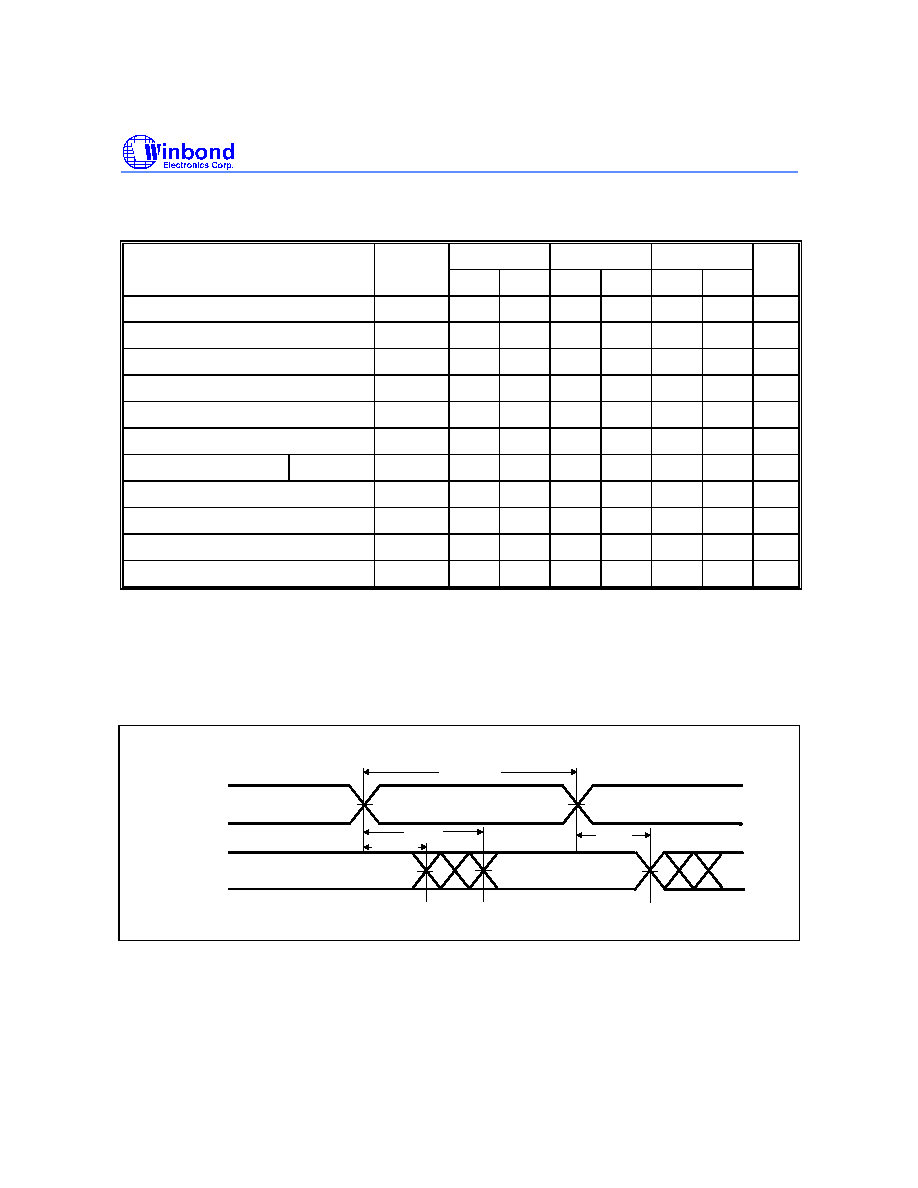
TIMING WAVEFORMS
Read Cycle 1
(Address Controlled, #CS = #OE = #UB = #LB = V
IL
,
#WE = V
IH
)
Address
T
T
T
T
D
OH
AA
RC
OH
OUT